| Citation: | CUI Bo-wen, YAO Zi-jun, CHEN Bing-gen, SHEN Ji, ZHANG Hai-feng, WU Shi-tan, WANG Zi-heng, ZHOU Jian, WANG Chen, HE Wei-ji, CHEN Yuan-jin. 2×2 silicon-based waveguide optical switch driven by mems electrostatic actuation[J]. Chinese Optics. doi: 10.37188/CO.2026-0055

|
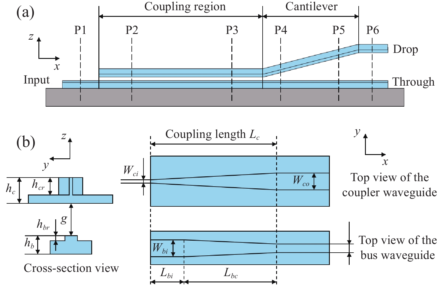
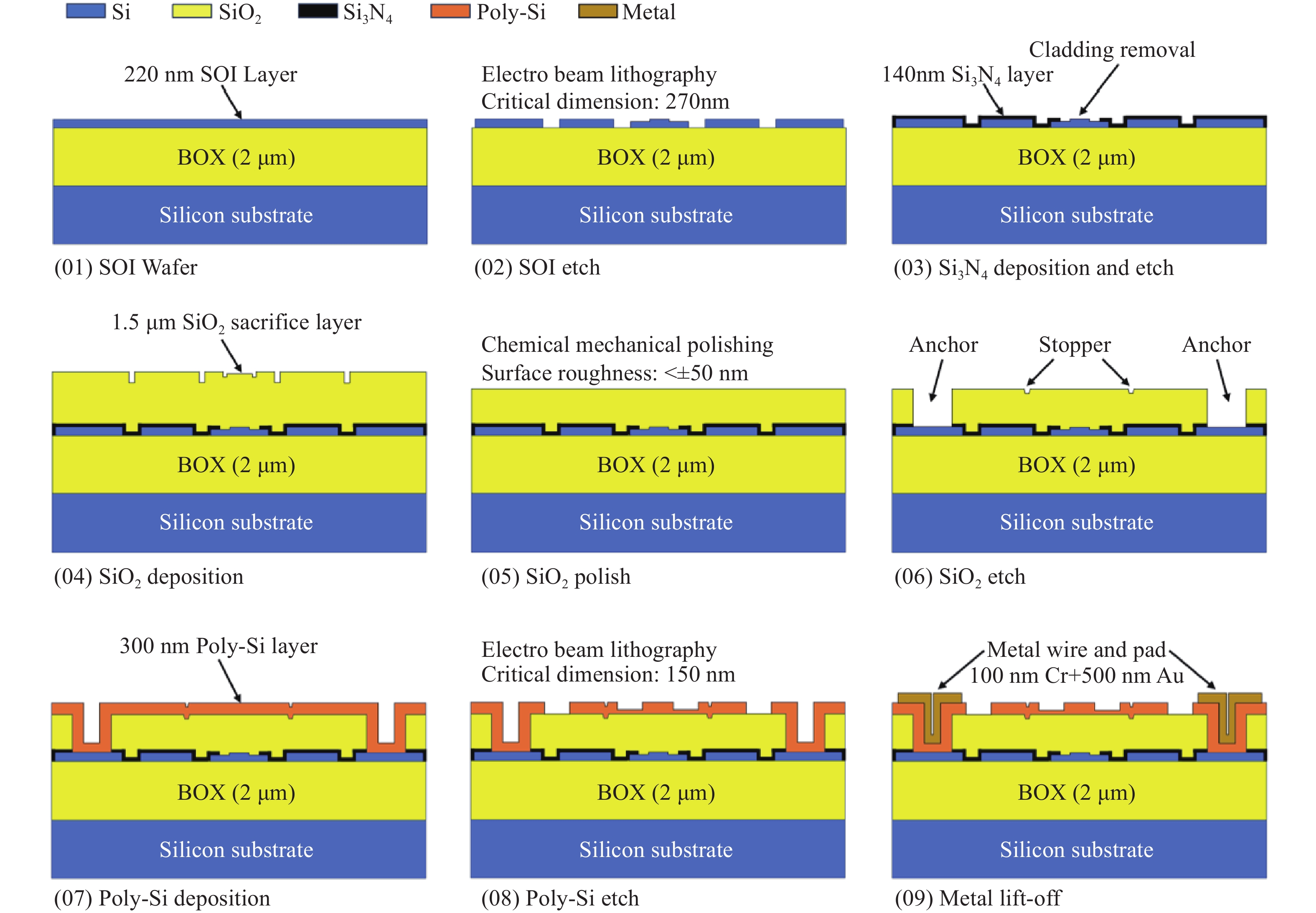
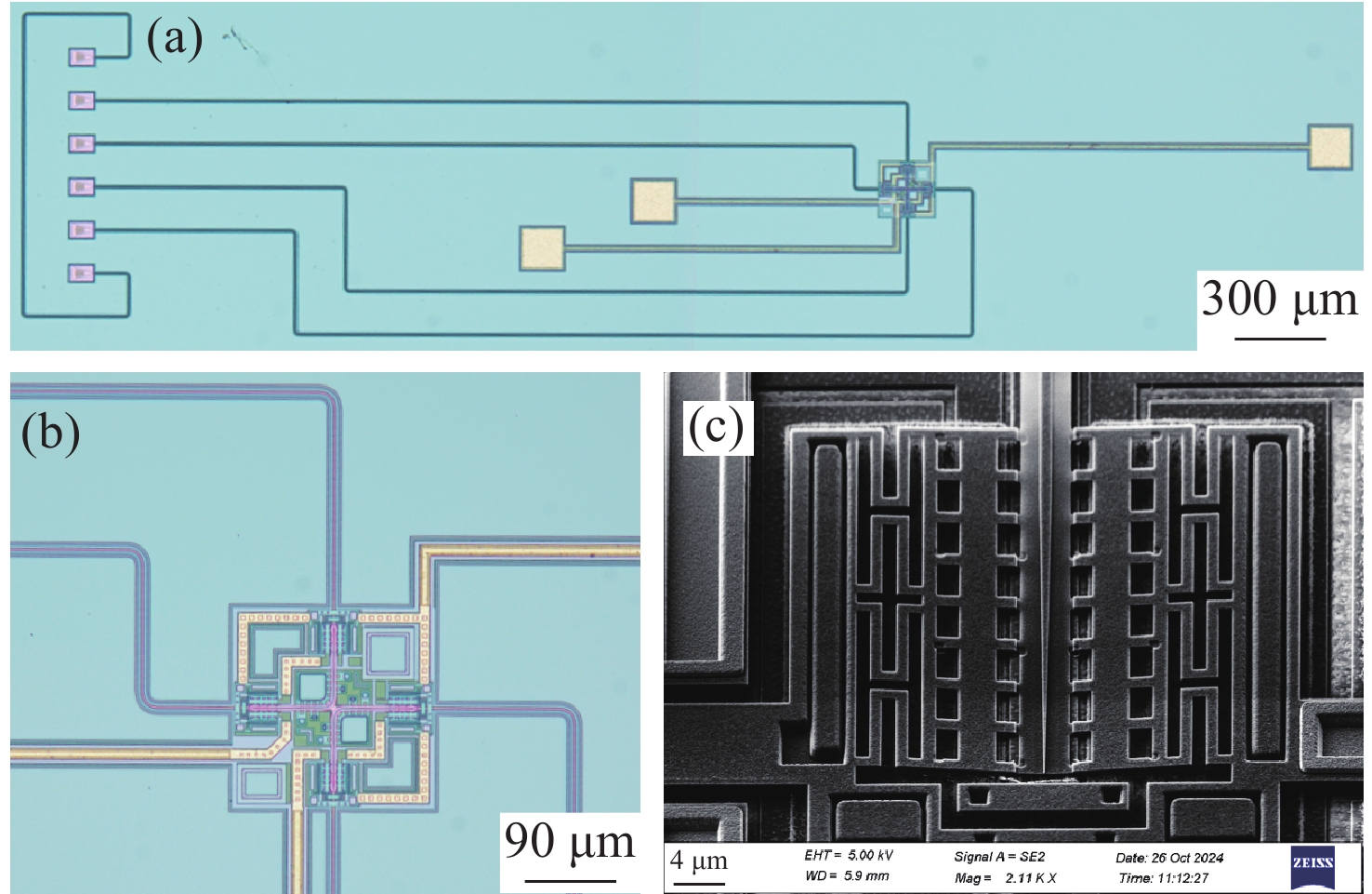
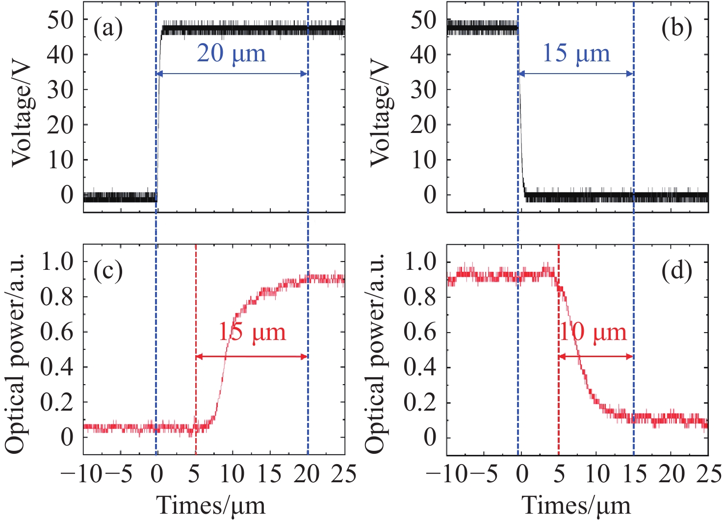
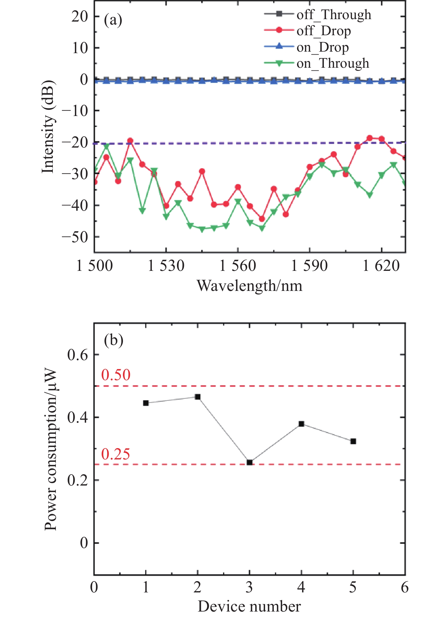
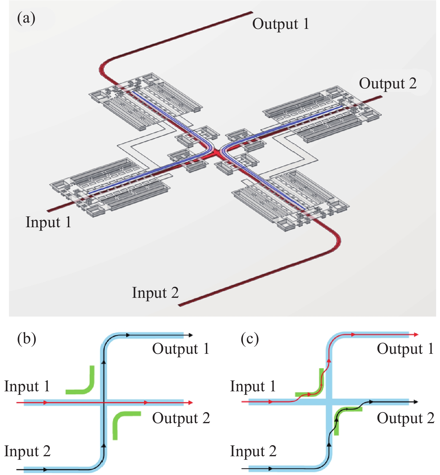
To overcome the limitations of current technologies, including the slow switching speed, heat accumulation, and high power consumption of thermo-optic waveguide switches, the high transmission loss of electro-optic waveguide switches, and the complex feedback control, difficulty in large-scale array integration, and narrow operating bandwidth commonly found in traditional photonic integrated circuit (PIC) waveguide switches, to meet the future demands of on-chip all-optical switching technologies for optical switches with fast response, low power consumption, broad bandwidth, low cost, and large-scale array fabrication capabilities, this study investigates micro-electro-mechanical systems (MEMS) driven silicon-based waveguide optical switch devices. By integrating silicon photonic waveguide technology with MEMS technology, we designed and fabricated an electrostatically driven MEMS 2×2 silicon waveguide optical switch (silicon photonic MEMS switch) capable of routing optical signals. The monolithic integration of silicon photonic waveguides and MEMS microactuators on a silicon wafer was achieved using electron-beam lithography combined with complementary metal-oxide-semiconductor (CMOS) processes. With a footprint of 192 μm × 192 μm, the device successfully demonstrated 2×2 optical switching functionality. The switching response times were measured at 20 μs and 15 μs, with optical signal rise and fall times of 15 μs and 10 μs, respectively. At a wavelength of

| [1] |
URATA R, LIU H, YASUMURA K, et al. Apollo: large-scale deployment of optical circuit switching for datacenter networking[C]. 2023 Optical Fiber Communications Conference and Exhibition (OFC), IEEE, 2023: 1-3.
|
| [2] |
URATA R, LIU H, YASUMURA K, et al. Mission Apollo: landing optical circuit switching at datacenter scale[J]. arXiv: 2208.10041, 2022. (查阅网上资料, 不确定文献类型及格式是否正确, 请核对).
|
| [3] |
WANG H, WANG ZH G, GONG CH, et al. Using light to image millimeter wave based on stacked meta-MEMS chip[J]. Light: Science & Applications, 2025, 14(1): 59.
|
| [4] |
RASTEGARFAR H. Optical switching in next-generation data centers[D]. Toronto: University of Toronto, 2014. (查阅网上资料, 未能确认本条文献修改是否正确, 请确认).
|
| [5] |
https://www.polatis.com/polatis-all-optical-switch-technology-lowest-loss-highest-performance-directlight-beam-steering.asp..
|
| [6] |
WANG X J, VAN MECHELEN T, BHARADWAJ S, et al. Exploiting universal nonlocal dispersion in optically active materials for spectro-polarimetric computational imaging[J]. eLight, 2024, 4(1): 22. doi: 10.1186/s43593-024-00078-2
|
| [7] |
高小勇, 刘阳阳, 胡光熹, 等. 基于马赫-曾德尔干涉仪的1×8硅基热光开关[J]. 光学学报, 2024, 44(8): 0813001. doi: 10.3788/AOS231782
GAO X Y, LIU Y Y, HU G X, et al. 1×8 Silicon-based thermo-optic switch based on Mach-Zehnder interferometers[J]. Acta Optica Sinica, 2024, 44(8): 0813001. (in Chinese). doi: 10.3788/AOS231782
|
| [8] |
程派. 低功耗平面光波导热光开关阵列的研究[D]. 长春: 吉林大学, 2025.
CHENG P. Study on low-power planar optical waveguide thermal optical switch array[D]. Changchun: Jilin University, 2025. (in Chinese).
|
| [9] |
WANG J, SHI SH Q, NIU H SH, et al. Ultrahigh extinction ratio and a low power silicon thermo-optic switch[J]. Optics Letters, 2024, 49(10): 2705-2708. doi: 10.1364/OL.520209
|
| [10] |
SUN B H, YAO CH H, LI T Y, et al. Tri-layer SiN-on-Si 8×8 optical switches with thermo-optic and electro-optic actuators[J]. Journal of Lightwave Technology, 2025, 43(11): 5400-5406. doi: 10.1109/JLT.2025.3545568
|
| [11] |
DING Y ZH, ZHANG D M, ZHANG P, et al. Dual-mode 2 × 2 electro-optic switch on a SOI platform[J]. Optics Letters, 2024, 49(21): 6125-6128. doi: 10.1364/OL.537380
|
| [12] |
WU Y T, CHU T. Low-crosstalk silicon optical switch with switching time<5.5ns[C]. 2025 30th OptoElectronics and Communications Conference (OECC) and 2025 International Conference on Photonics in Switching and Computing (PSC), IEEE, 2025: 1-4.
|
| [13] |
ZHOU J J, LV L M, YAO ZH SH, et al. High-performance thin-film lithium Niobate Mach–Zehnder modulator on 8-inch silicon substrates[J]. IEEE Photonics Technology Letters, 2024, 36(17): 1077-1080. doi: 10.1109/LPT.2024.3434542
|
| [14] |
LI Q Y, YI Q Y, SUN A L, et al. Ultra-broadband near- to mid-infrared electro-optic modulator on thin-film lithium niobate[J]. Nature Communications, 2026, 17(1): 1138. doi: 10.1038/s41467-025-67902-2
|
| [15] |
SEOK T J, QUACK N, HAN S, et al. Large-scale broadband digital silicon photonic switches with vertical adiabatic couplers[J]. Optica, 2016, 3(1): 64-70. doi: 10.1364/OPTICA.3.000064
|
| [16] |
HU Y P, SUN Y, LU Y, et al. Silicon photonic MEMS switches based on split waveguide crossings[J]. Nature Communications, 2025, 16(1): 331. doi: 10.1038/s41467-024-55528-9
|
| [17] |
杜立群, 李奥奇, 李蒙, 等. 双向高过载硅基差压敏感元件的研制[J]. 光学 精密工程, 2025, 33(2): 209-219. doi: 10.37188/OPE.20253302.0209
DU L Q, LI A Q, LI M, et al. Development of bi-directional high overload silicon-based differential pressure sensitive element[J]. Optics and Precision Engineering, 2025, 33(2): 209-219. (in Chinese). doi: 10.37188/OPE.20253302.0209
|
Figures(9)


 DownLoad: