| Citation: | GAO Chen, CHEN Lin, ZHANG Zhong-yin, ZHANG Guo-dong, WANG Jiang, CHENG Guang-hua. Study onnanoscale etching of silicon carbide for deep-subwavelength features based on spatiotemporally shaped ultrafast laser pulses[J]. Chinese Optics. doi: 10.37188/CO.2026-0054

|
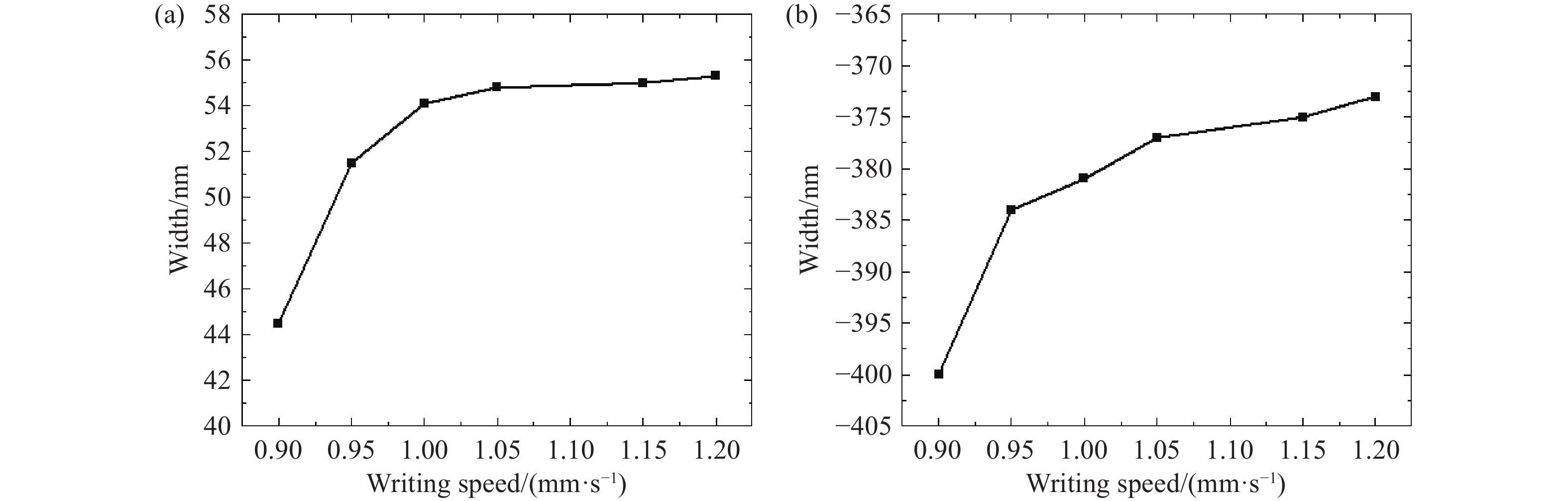
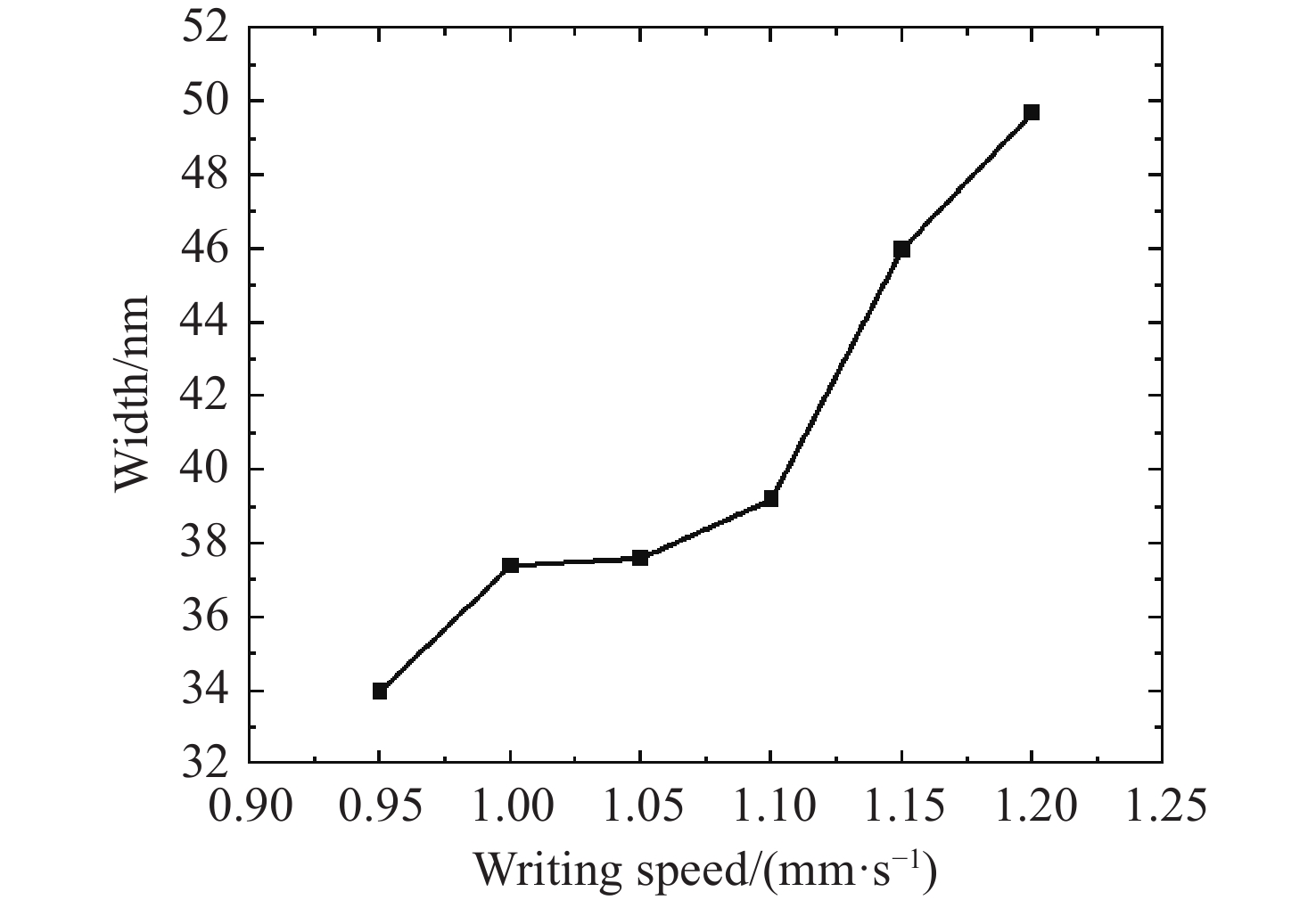
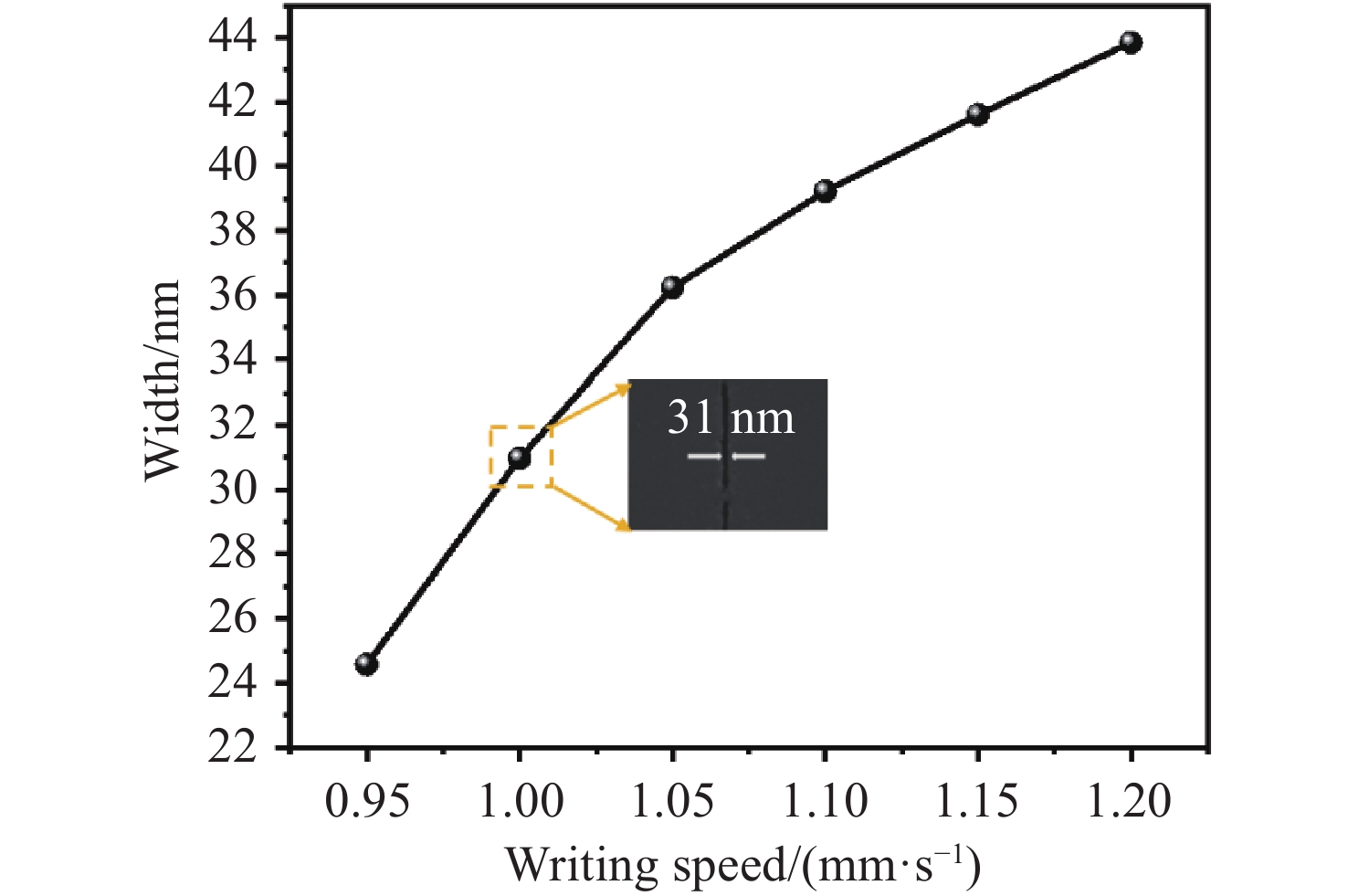
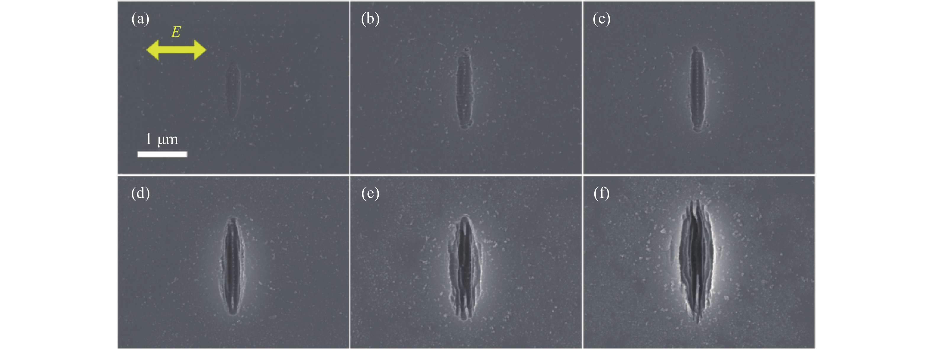
Femtosecond-laser-induced self-organized interference, together with near-field enhancement and incubation effects, enables deep-subwavelength nanoetching. However, the formation of such structures usually relies on random surface scattering centers and multi-pulse feedback, leading to poor uniformity, limited repeatability, and high sensitivity to laser parameters. In this work, a spatiotemporal laser-energy modulation strategy is proposed to improve the writing quality of nanogrooves on 4H-SiC single-crystal surfaces. In the spatial domain, single-slit and double-slit beam shaping are employed to reconstruct the focal-plane energy distribution, suppress lateral energy spreading, and enhance the incubation and self-organized interference effects. In the temporal domain, a GHz burst mode is introduced to regulate the energy-deposition sequence, reduce the instantaneous energy-deposition intensity, and extend the annealing time. Static irradiation and dynamic scanning experiments were conducted to systematically investigate the surface morphology evolution and nanogroove formation mechanism under different modulation strategies. The results show that the elliptical focal spot formed by single-slit shaping enhances the incubation and annealing effects, producing nanogrooves with improved uniformity and edge regularity and a minimum groove width of 62 nm. Double-slit shaping further strengthens the interference-field confinement, reduces the dependence of nanogroove formation on random scattering centers, and decreases the minimum controllable groove width to 34 nm. By introducing GHz burst pulses on the basis of double-slit shaping, stepwise energy deposition through sub-pulses with a 400 ps interval reduces instantaneous strong excitation and suppresses molten redeposition and particle attachment, further decreasing the minimum controllable groove width to 24.5 nm. This spatiotemporal modulation strategy provides an effective technical approach and theoretical basis for high-precision, low-damage, and highly repeatable nanomanufacturing on third-generation semiconductor surfaces.

| [1] |
BERESNA M, KAZANSKY P G. Polarization diffraction grating produced by femtosecond laser nanostructuring in glass[J]. Optics Letters, 2010, 35(10): 1662-1664. doi: 10.1364/OL.35.001662
|
| [2] |
BERESNA M, GECEVIČIUS M, KAZANSKY P G. Polarization sensitive elements fabricated by femtosecond laser nanostructuring of glass [Invited][J]. Optical Materials Express, 2011, 1(4): 783-795. doi: 10.1364/OME.1.000783
|
| [3] |
DREVINSKAS R, KAZANSKY P G. High-performance geometric phase elements in silica glass[J]. APL Photonics, 2017, 2(6): 066104. doi: 10.1063/1.4984066
|
| [4] |
DREVINSKAS R, BERESNA M, ZHANG J Y, et al. Ultrafast laser‐induced metasurfaces for geometric phase manipulation[J]. Advanced Optical Materials, 2017, 5(1): 1600575. doi: 10.1002/adom.201600575
|
| [5] |
MINGAREEV I, HORN A. Time-resolved investigations of plasma and melt ejections in metals by pump-probe shadowgrpahy[J]. Applied Physics A, 2008, 92(4): 917-920. doi: 10.1007/s00339-008-4562-7
|
| [6] |
PHILLIPS K C, GANDHI H H, MAZUR E, et al. Ultrafast laser processing of materials: a review[J]. Advances in Optics and Photonics, 2015, 7(4): 684-712. doi: 10.1364/AOP.7.000684
|
| [7] |
SIPE J E, YOUNG J F, PRESTON J S, et al. Laser-induced periodic surface structure. I. Theory[J]. Physical Review B, 1983, 27(2): 1141-1154. doi: 10.1103/PhysRevB.27.1141
|
| [8] |
MIYAJI G, MIYAZAKI K. Origin of periodicity in nanostructuring on thin film surfaces ablated with femtosecond laser pulses[J]. Optics Express, 2008, 16(20): 16265-16271. doi: 10.1364/OE.16.016265
|
| [9] |
BONSE J, KRÜGER J, HÖHM S, et al. Femtosecond laser-induced periodic surface structures[J]. Journal of Laser Applications, 2012, 24(4): 042006. doi: 10.2351/1.4712658
|
| [10] |
BIRNBAUM M. Semiconductor surface damage produced by ruby lasers[J]. Journal of Applied Physics, 1965, 36(11): 3688-3689. doi: 10.1063/1.1703071
|
| [11] |
SHIMOTSUMA Y, KAZANSKY P G, QIU J R, et al. Self-organized nanogratings in glass irradiated by ultrashort light pulses[J]. Physical Review Letters, 2003, 91(24): 247405. doi: 10.1103/PhysRevLett.91.247405
|
| [12] |
BHARDWAJ V R, SIMOVA E, RAJEEV P P, et al. Optically produced arrays of planar nanostructures inside fused silica[J]. Physical Review Letters, 2006, 96(5): 057404. doi: 10.1103/PhysRevLett.96.057404
|
| [13] |
TAYLOR R, HNATOVSKY C, SIMOVA E. Applications of femtosecond laser induced self-organized planar nanocracks inside fused silica glass[J]. Laser & Photonics Reviews, 2008, 2(1-2): 26-46. doi: 10.1002/lpor.200710031
|
| [14] |
LI ZH Z, WANG L, FAN H, et al. O-FIB: far-field-induced near-field breakdown for direct nanowriting in an atmospheric environment[J]. Light: Science & Applications, 2020, 9(1): 41.
|
| [15] |
ZHANG G D, RUDENKO A, STOIAN R, et al. Ultrafast laser high-aspect-ratio extreme nanostructuring of glass beyond λ/100[J]. Ultrafast Science, 2025, 5: 0103. doi: 10.34133/ultrafastscience.0103
|
| [16] |
CHANAL M, FEDOROV V Y, CHAMBONNEAU M, et al. Crossing the threshold of ultrafast laser writing in bulk silicon[J]. Nature Communications, 2017, 8(1): 773. doi: 10.1038/s41467-017-00907-8
|
| [17] |
WANG A D, DAS A, GROJO D. Ultrafast laser writing deep inside silicon with THz-repetition-rate trains of pulses[J]. Research, 2020, 2020: 8149764. doi: 10.34133/2020/8149764
|
| [18] |
LIU M T, LU B L, LV J, et al. Polarization-dependent anisotropy of LIPSSs’ morphology evolution on a single-crystal silicon surface[J]. Micromachines, 2024, 15(2): 200. doi: 10.3390/mi15020200
|
| [19] |
GUO X, PENG Z Y, DING P B, et al. Nonlinear optical properties of 6H-SiC and 4H-SiC in an extensive spectral range[J]. Optical Materials Express, 2021, 11(4): 1080-1092. doi: 10.1364/OME.415915
|
| [20] |
REITANO R, BAERI P. Excimer laser induced thermal evaporation and ablation of silicon carbide[J]. Nuclear Instruments and Methods in Physics Research Section B: Beam Interactions with Materials and Atoms, 1996, 116(1-4): 369-372. doi: 10.1016/b978-0-444-82412-7.50055-9
|
| [21] |
ZHANG R, HUANG CH ZH, WANG J, et al. Micromachining of 4H-SiC using femtosecond laser[J]. Ceramics International, 2018, 44(15): 17775-17783. doi: 10.1016/j.ceramint.2018.06.245
|
| [22] |
OBARA G, SHIMIZU H, ENAMI T, et al. Growth of high spatial frequency periodic ripple structures on SiC crystal surfaces irradiated with successive femtosecond laser pulses[J]. Optics Express, 2013, 21(22): 26323-26334. doi: 10.1364/OE.21.026323
|
| [23] |
NAN L, MANCINI A, WEBER T, et al. Angular dispersion suppression in deeply subwavelength phonon polariton bound states in the continuum metasurfaces[J]. Nature Photonics, 2025, 19(6): 615-623. doi: 10.1038/s41566-025-01670-9
|
| [24] |
LIN ZH Y, LIU H G, JI L F, et al. Realization of ~ 10 nm features on semiconductor surfaces via femtosecond laser direct patterning in far field and in ambient air[J]. Nano Letters, 2020, 20(7): 4947-4952. doi: 10.1021/acs.nanolett.0c01013
|
| [25] |
ZHANG Y CH, JIANG Q L, CAO K Q, et al. Extremely regular periodic surface structures in a large area efficiently induced on silicon by temporally shaped femtosecond laser[J]. Photonics Research, 2021, 9(5): 839-847. doi: 10.1364/PRJ.418937
|
| [26] |
LONG M Q, HAN R ZH, CAO K Q, et al. High-quality diffractive optical elements on sapphire efficiently processed using shaped femtosecond laser[J]. Photonics Research, 2026, 14(4): 1299-1313. doi: 10.1364/PRJ.576398
|
| [27] |
LI K, HAN R ZH, SUO M Q, et al. High quality nanogratings far beyond diffraction limits on silicon efficiently fabricated using femtosecond laser dual-beam interference direct writing[J]. Optics & Laser Technology, 2025, 181: 111505. doi: 10.1016/j.optlastec.2024.111505
|
Figures(6)




 DownLoad: