



Fabrication and ultraviolet detection performance of ZnO NRs/Porous GaN heterojunction
doi: 10.37188/CO.EN-2026-0016
-
摘要:
由于传统ZnO/GaN异质结紫外光电探测器仍存在界面接触面积有限、载流子输运效率不足以及ZnO本征缺陷影响光电响应的问题,限制了器件性能的进一步提升。因此本文采用低温水热法在多孔p-GaN/Al2O3衬底上生长了不同Ga掺杂浓度的Ga+Al共掺杂ZnO纳米棒阵列,并制备了相应的Ga+Al共掺杂ZnO纳米棒/多孔GaN异质结,通过多孔p-GaN增强异质结界面接触与光吸收,并利用Ga+Al共掺杂调控ZnO纳米棒的缺陷状态和载流子输运性能,从而提高器件的自供电紫外探测性能。结果表明,在0 V偏压和365 nm紫外光照下,Ga掺杂浓度为3%时器件表现出最佳的紫外探测性能,其光暗电流比为
8250 、响应度(R )为0.158 A/W、比探测率(D *)为3.15×10¹² Jones、外量子效率(EQE )为53.5%。该研究为制备下一代高性能ZnO/GaN基异质结紫外光电探测器提供了一定的理论指导和实验数据。-
关键词:
- 多孔GaN /
- 低温水热法 /
- ZnO纳米棒 /
- ZnO纳米棒/GaN异质结 /
- 紫外光电探测器
Abstract:Owing to the limited interfacial contact area, insufficient carrier transport efficiency, and the adverse effects of intrinsic defects in ZnO on photoresponse, further improvement in the performance of conventional ZnO/GaN heterojunction ultraviolet photodetectors remains restricted. To address these issues, Ga+Al co-doped ZnO nanorod arrays with different Ga doping concentrations were grown on porous p-GaN/Al2O3 substrates by a low-temperature hydrothermal method, and the corresponding Ga+Al co-doped ZnO nanorod/porous GaN heterojunctions were fabricated. The porous p-GaN structure was used to enhance heterojunction interfacial contact and light absorption, while Ga+Al co-doping was employed to regulate the defect states and carrier transport properties of ZnO nanorods, thereby improving the self-powered ultraviolet photodetection performance of the devices. The findings of the study demonstrated that under 365 nm ultraviolet illumination at 0 V bias, the device with a Ga doping concentration of 3 at.% exhibited the best UV photodetection performance, with a light/dark current ratio of
8250 , a responsivity (R ) of 0.158 A/W, a specific detectivity (D *) of 3.15×10¹² Jones, and an external quantum efficiency (EQE ) of 53.5%. This study provides useful theoretical insight and experimental support for the development of next-generation high-performance ZnO/GaN-based heterojunction ultraviolet photodetectors. -
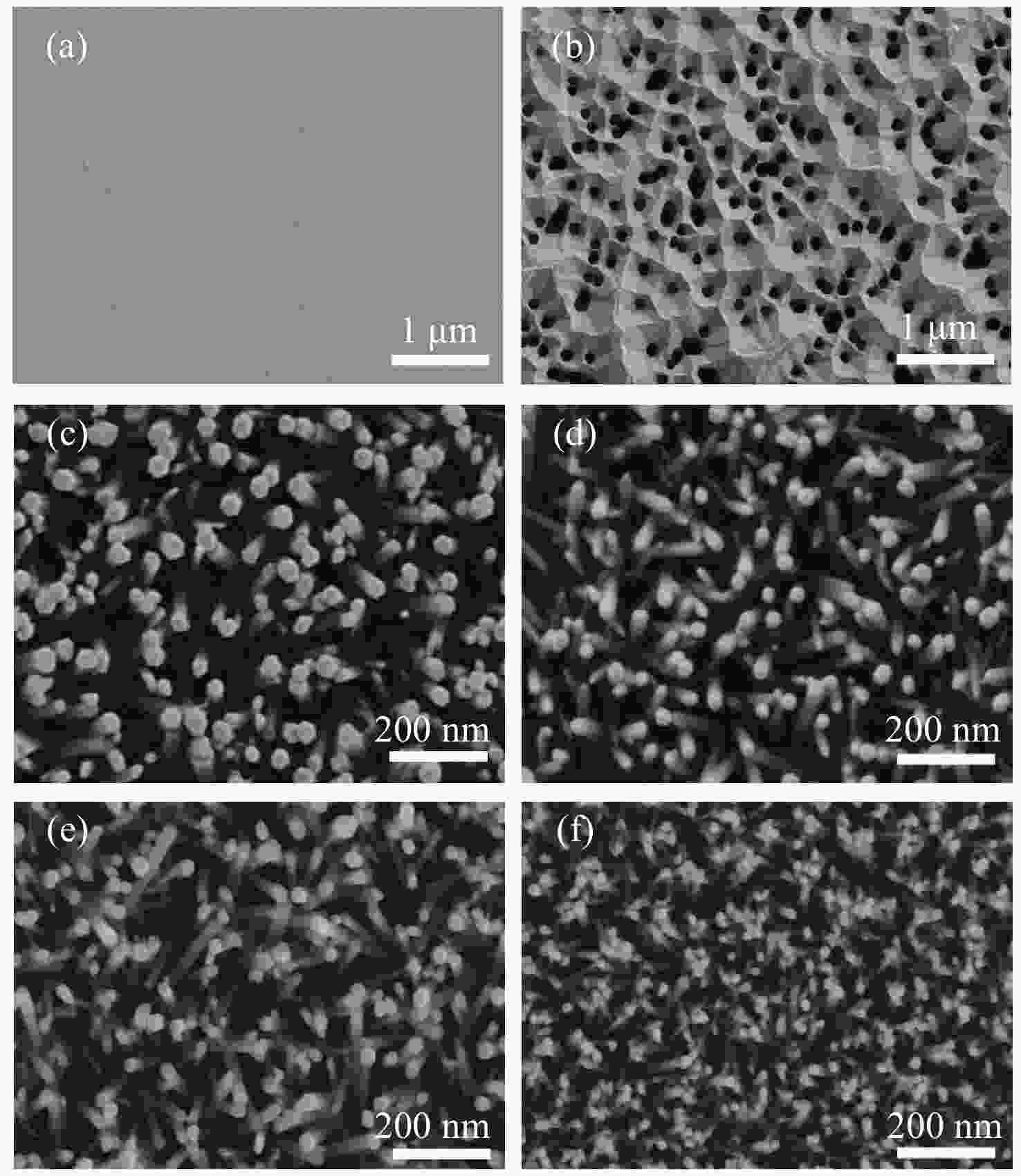
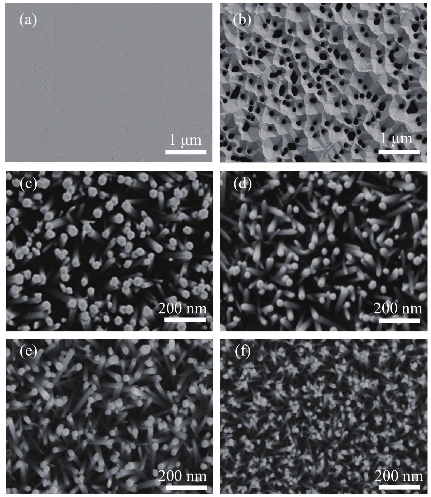
Figure 2. SEM images of porous p-GaN films (a,b);Top-view SEM images of Ga+Al co-doped ZnO NRs/porous GaN with different Ga doping concentrations:(c) S0; (d) S1; (e) S2; and (f) S3.
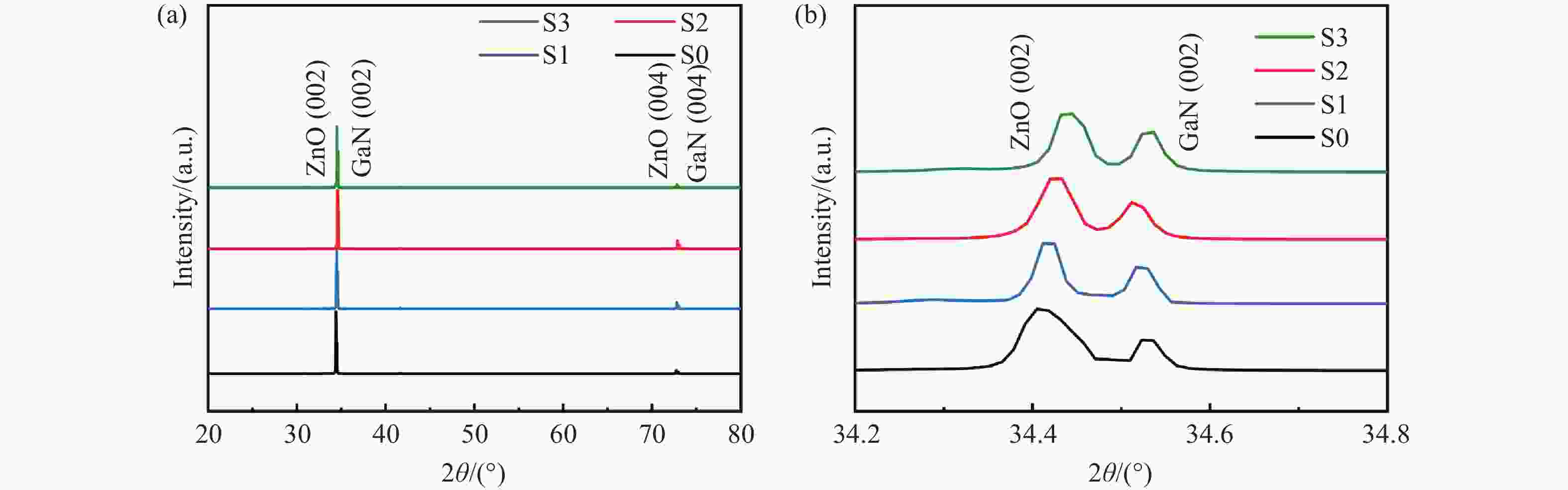
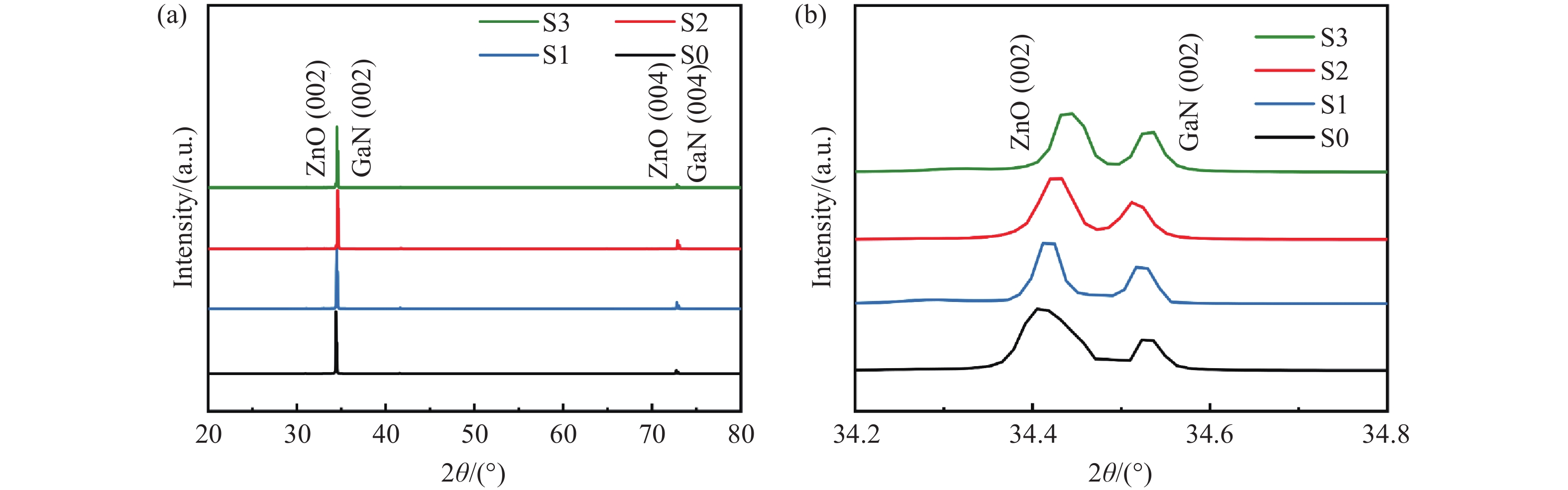
Figure 3. XRD patterns of Ga+Al co-doped ZnO NRs/porous GaN heterojunctions with different Ga doping concentrations.
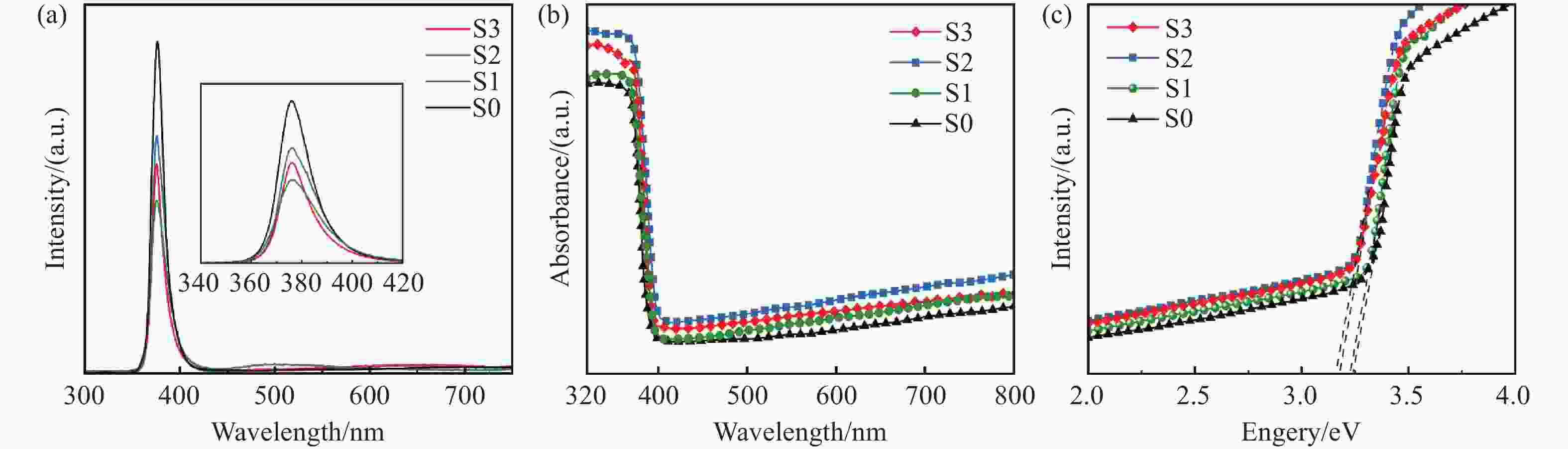
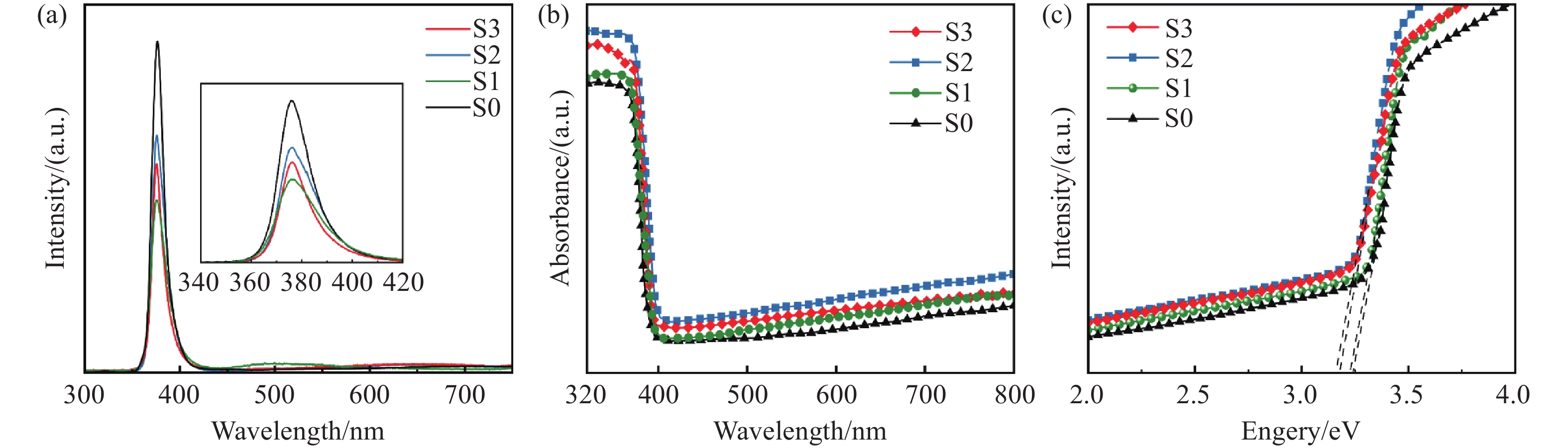
Figure 4. (a) Photoluminescence spectra; (b) UV-visible absorption spectra; and (c) Tauc plots of Ga+Al co-doped ZnO NRs/porous GaN heterojunctions with different Ga doping concentrations.
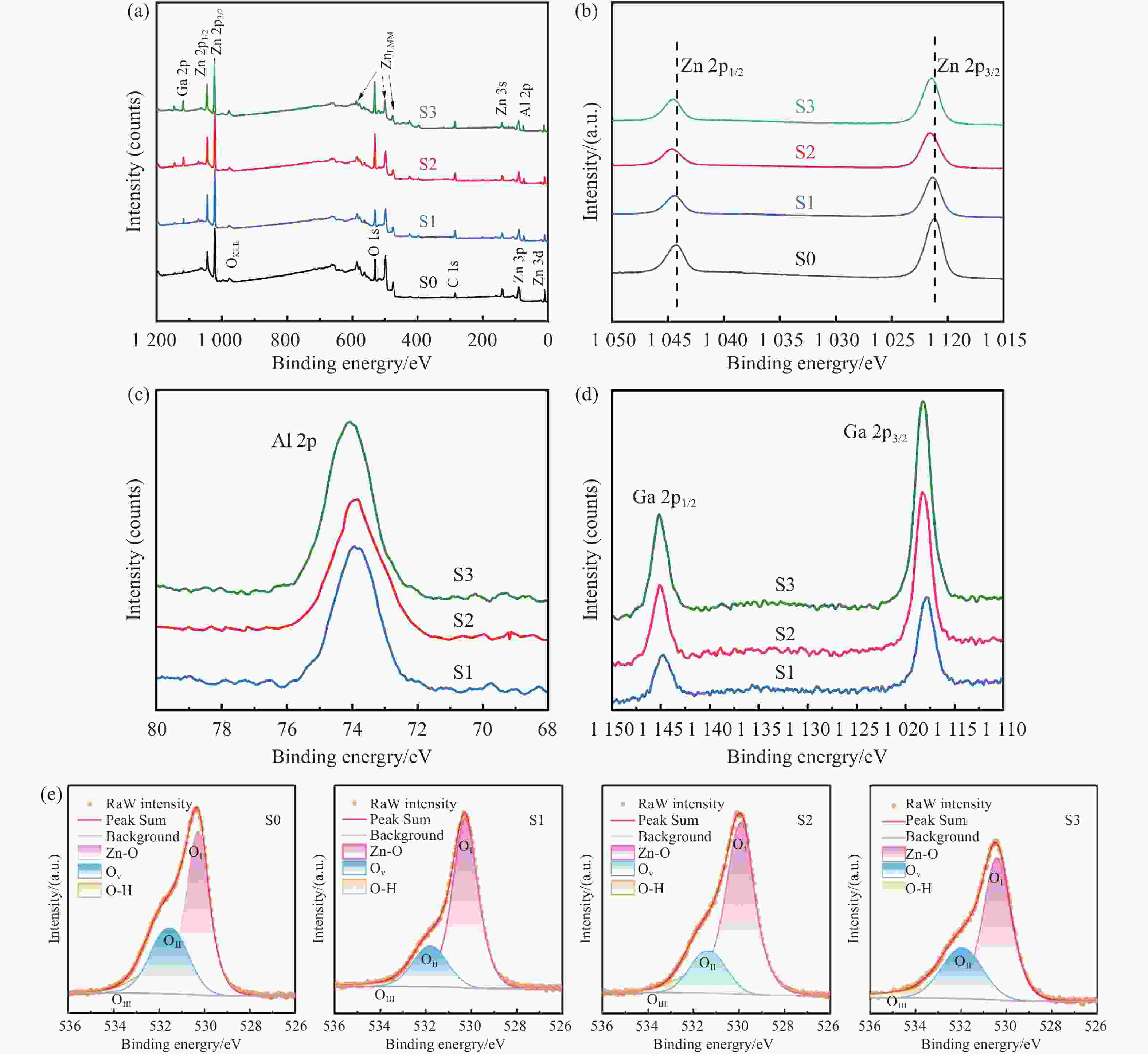
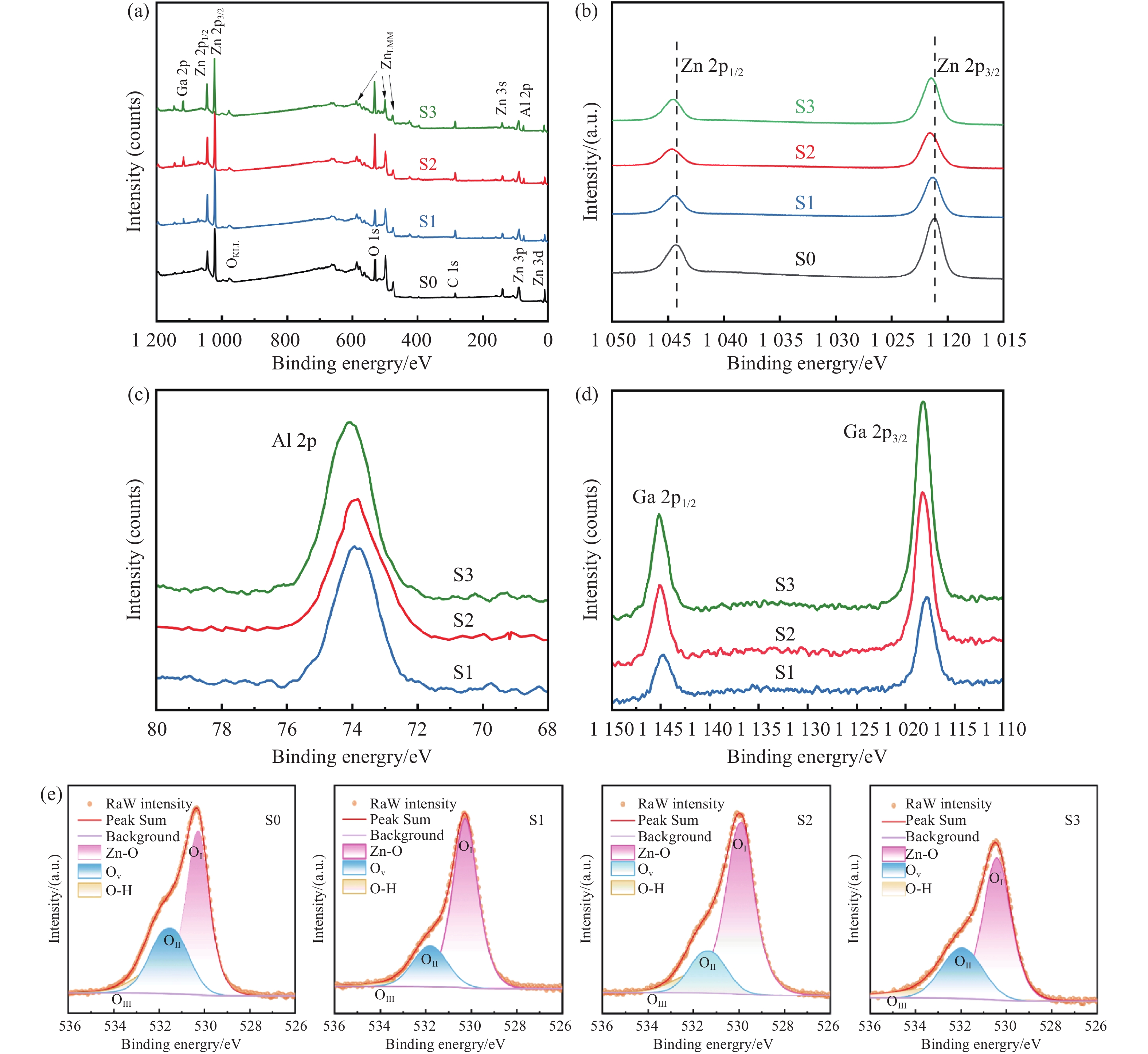
Figure 5. XPS spectra of Ga+Al co-doped ZnO NRs/porous GaN heterojunctions with different Ga doping concentrations: (a) survey spectra; (b) Zn 2p spectra; (c) Al 2p spectra; (d) Ga 2p spectra, and (e) O1s spectra.
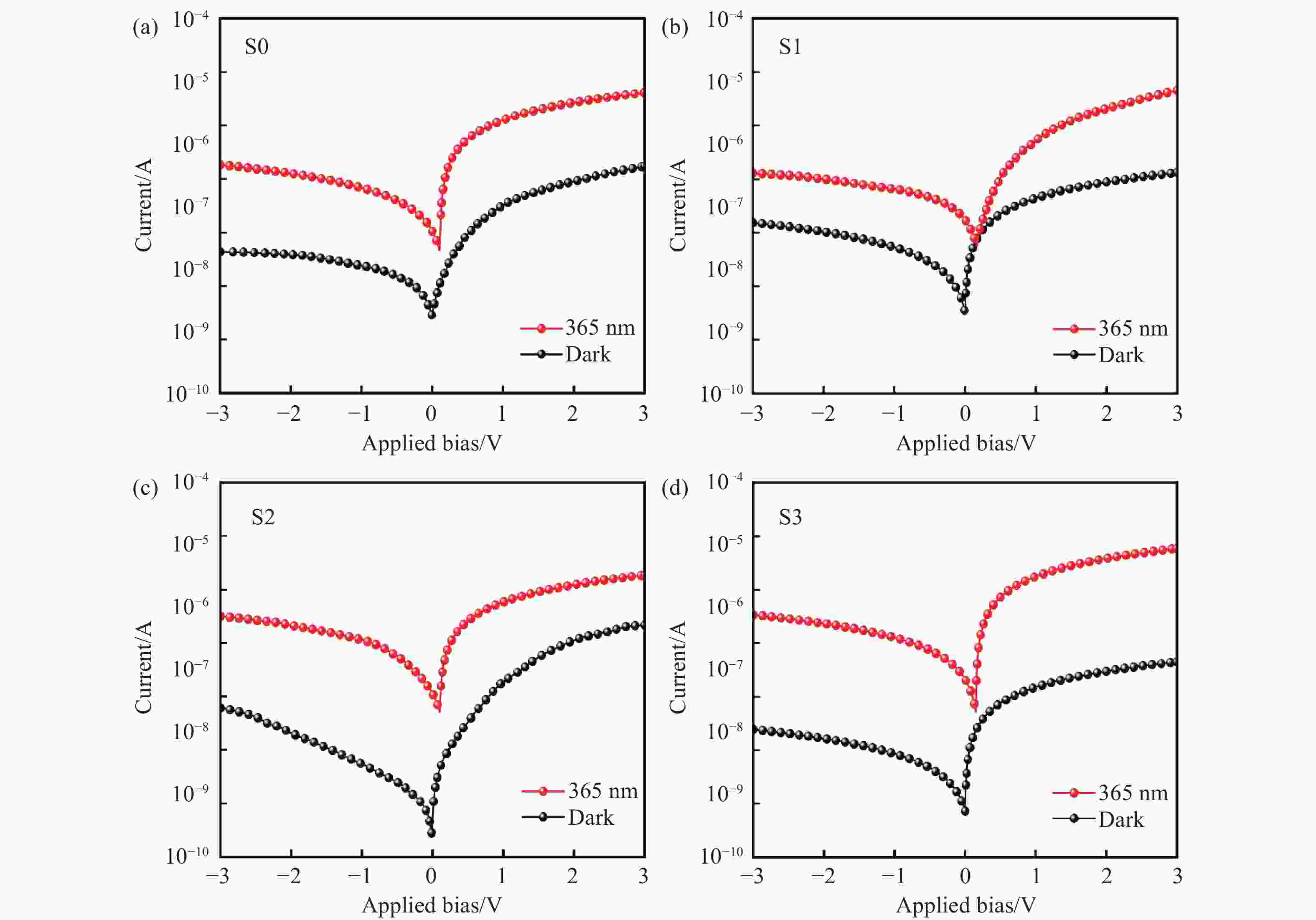
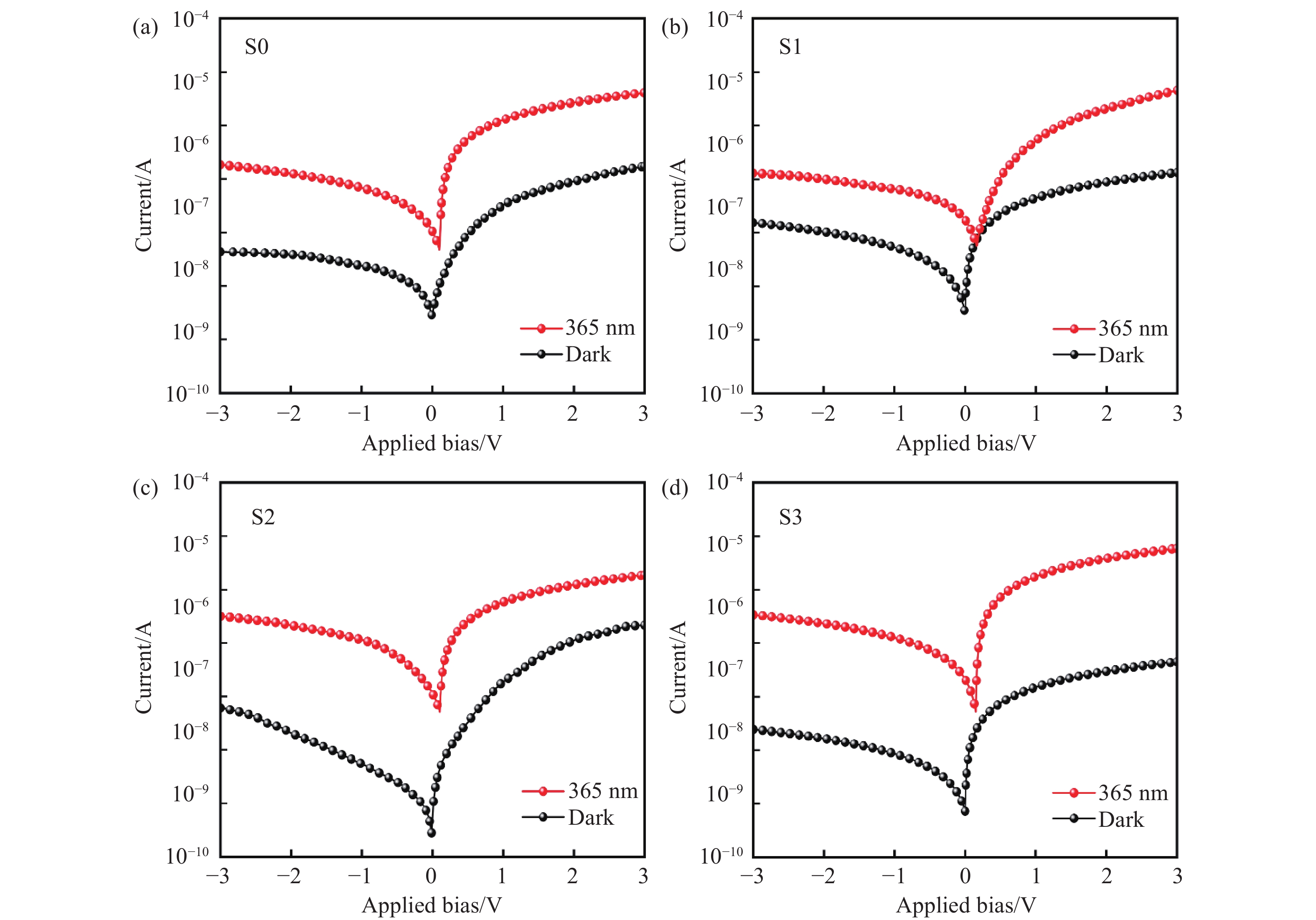
Figure 6. I-V characteristics of Ga+Al co-doped ZnO NRs/porous GaN heterojunctions with different Ga doping concentrations: (a)S0; (b)S1; (c)S2; (d)S3.
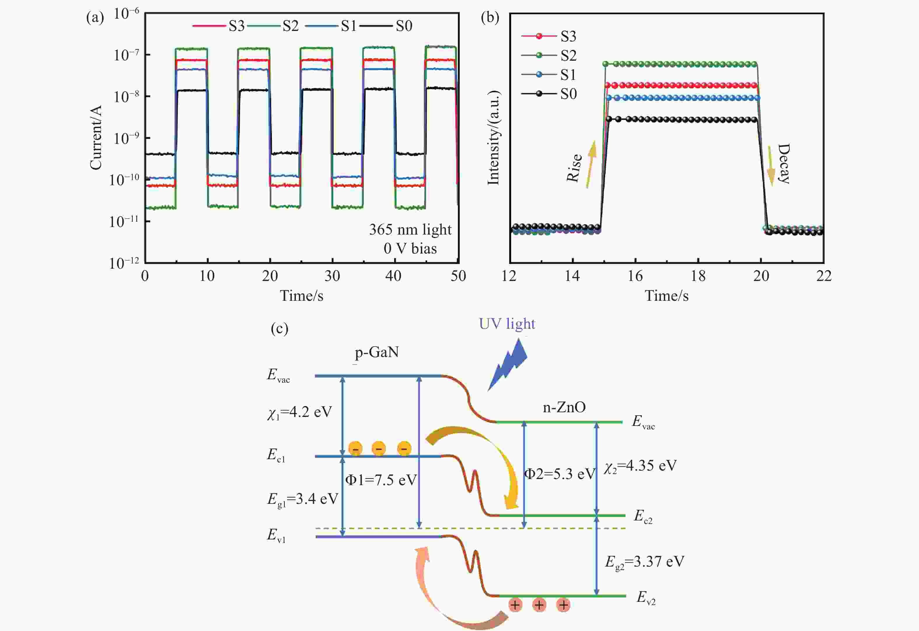
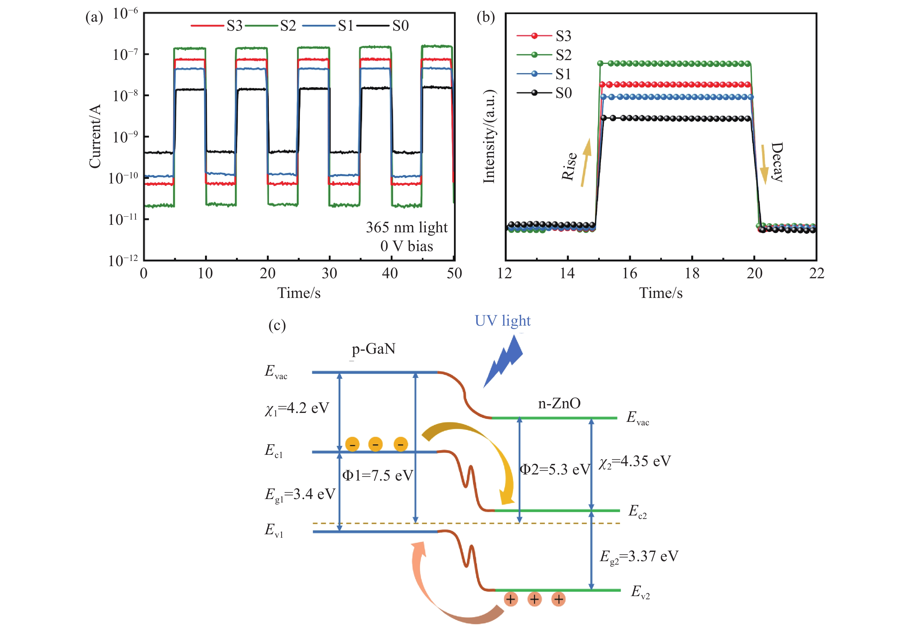
Figure 7. (a) I-t characteristic curves and (b) time response curves of Ga+Al co-doped ZnO NRs/porous GaN heterojunctions with different Ga doping concentrations under zero bias and 365 nm illumination; (c) Energy band diagrams of ZnO/GaN heterojunction.
Table 1. Performance comparison of the ZnO NRs/porous GaN heterojunction photodetector (sample S2) and other reported ZnO/GaN based photodetectors under 0 V bias.
Photodetector λ (nm) R (mA/W) D* (Jones) EQE (%) Reference P-GaN/n-ZnO film 368 11 6.2×10¹¹ 3.71 [22] P-GaN/n-ZnO NRs 365 138.9 1012 47.6 [39] P-GaN/n-ZnO microwire 370 137 2.15×10¹² 45.9 [3] P-GaN/n-ZnO:Ga NRs 365 230 2.32×10¹² [40] P-GaN/n-ZnO: In+La film 366 46 9.92×10¹¹ 15.6 [26] P-GaN/n-ZnO:Ga+In NRs 5.29 7.98×10⁹ 1.79 [27] Porous p-GaN/n-ZnO:Ga+Al NRs 365 158 3.15×10¹² 53.5 This work  下载: 导出CSV
-
[1] LIN·H W, JIANG·A, XING·SH B, et al. Advances in self-powered ultraviolet photodetectors based on P-N heterojunction low-dimensional nanostructures[J]. Nanomaterials, 2022, 12(6): 910. doi: 10.3390/nano12060910 [2] HOU·X H, ZHAO·X L, ZHANG·Y, et al. High-performance harsh-environment-resistant GaOx solar-blind photodetectors via defect and doping engineering[J]. Advanced Materials, 2022, 34: 2106923. doi: 10.1002/adma.202106923 [3] XIE·Y L, WAN·P, JIANG·M M, et al. Performance enhancement of a self-biased n-ZnO microwire/p-GaN heterojunction ultraviolet photodetector incorporating Ag nanowires[J]. CrystEngComm, 2022, 24: 7727-7738. doi: 10.1039/D2CE01084D [4] CAO·F, LIU·Y, LIU·M, et al. Wide bandgap semiconductors for ultraviolet photodetectors: approaches, applications, and prospects[J]. Research, 2024, 7: 0385. doi: 10.34133/research.0385 [5] XIAO·Y, LIU·L, MA·ZH·H, et al. High-performance self-powered ultraviolet photodetector based on Nano-porous GaN and CoPc p-n vertical heterojunction[J]. Nanomaterials, 2019, 9(9): 1198. doi: 10.3390/nano9091198 [6] JIA·K D, JIA·W, LI·T B, et al. Fabrication of porous CuxZn1-xS/GaN heterojunctions for ultraviolet photodetector application[J]. Optical Materials, 2025, 162: 116881. doi: 10.1016/j.optmat.2025.116881 [7] WEN·J J, WANG·Y K, ZHANG·B, et al. High-performance ultraviolet photodetectors based on nanoporous GaN with a Ga2O3 single-crystal layer[J]. Nanomaterials, 2024, 14(13): 1165. doi: 10.3390/nano14131165 [8] CUI·J SH, ZHOU·J P, CHEN·H M, et al. Effect of ultraviolet and room lights on porous GaN films using photo-assisted electrochemical etching[J]. Materials Letters, 2021, 301: 130287. doi: 10.1016/j.matlet.2021.130287 [9] CHEN·C·H, CHANG·S·J, SU·Y·K, et al. Vertical high quality mirrorlike facet of GaN-based device by reactive ion etching[J]. Japanese Journal of Applied Physics, 2001, 40: 2762-2764. doi: 10.1143/JJAP.40.2762 [10] ZHANG·L, WANG·SH ZH, SHAO·Y L, et al. One-step fabrication of porous GaN crystal membrane and its application in energy storage[J]. Scientific Reports, 2017, 7: 44063. doi: 10.1038/srep44063 [11] CHEN·R R, LIU·J, FENG·B, et al. Pores in p-type GaN by annealing under nitrogen atmosphere: formation and photodetector[J]. Journal of Materials Science, 2022, 57(1): 467-476. doi: 10.1007/s10853-021-06632-4 [12] MENG R L, JI·X L, LOU·ZH, et al. High-performance nanoporous-GaN metal-insulator-semiconductor ultraviolet photodetectors with a thermal oxidized β-Ga2O3 layer[J]. Optics Letters, 2019, 44(9): 2197-2200. doi: 10.1364/OL.44.002197 [13] YU·R X, WANG·G D, SHAO·Y L, et al. From bulk to porous GaN crystal: precise structural control and its application in ultraviolet photodetectors[J]. Journal of Materials Chemistry C, 2019, 7(45): 14116-14122. doi: 10.1039/C9TC04820K [14] PU·T F, YOUNIS·U, CHIU·H·C, et al. Review of recent progress on vertical GaN-based PN diodes[J]. Nanoscale Research Letters, 2021, 16: 101. doi: 10.1186/s11671-021-03554-7 [15] NOMOTO·K, SONG·B, HU·Z Y, et al. 1.7-kV and 0.55 mΩ·cm2 GaN p-n diodes on bulk GaN substrates with avalanche capability[J]. IEEE Electron Device Letters, 2016, 37(2): 161-164. doi: 10.1109/LED.2015.2506638 [16] GUO·Y, SUN·Y·M, SONG·W·D. Narrowband near-ultraviolet photodetector fabricated from porous GaN/CuZnS heterojunction[J]. Acta Physica Sinica, 2022, 71(21): 218501. doi: 10.7498/aps.71.20220990 [17] VARSHNEY·U, SHARMA·A, VASHISHTHA·P, et al. Ga2O3/GaN heterointerface-based self-driven broad-band ultraviolet photodetectors with high responsivity[J]. ACS Applied Electronic Materials, 2022, 4(11): 5641-5651. doi: 10.1021/acsaelm.2c01362 [18] ZHANG·J T, TANG·K, WEI·T CH, et al. High-photosensitive ultraviolet photodetector based on an n-ZnO microwire/p-InGaN heterojunction[J]. Physica E: Low-dimensional Systems and Nanostructures, 2023, 146: 115562. doi: 10.1016/j.physe.2022.115562 [19] JIN·Y M, JIAO·SH, WANG·D B, et al. Enhanced UV photoresponsivity of ZnO nanorods decorated with Ag2S/ZnS nanoparticles by successive ionic layer adsorption and reaction method[J]. Nanomaterials, 2021, 11(2): 461. doi: 10.3390/nano11020461 [20] BAKRY·M, ISMAIL·W, ABDELFATAH·M, et al. Low-cost fabrication methods of ZnO nanorods and their physical and photoelectrochemical properties for optoelectronic applications[J]. Scientific Reports, 2024, 14: 23788. doi: 10.1038/s41598-024-73352-5 [21] HONG·S·K, KO·H·J, CHEN·Y F, et al. Defect characterization in epitaxial ZnO/epi-GaN/Al2O3 heterostructures: transmission electron microscopy and triple-axis X-ray diffractometry[J]. Journal of Crystal Growth, 2000, 209(2-3): 537-541. doi: 10.1016/S0022-0248(99)00615-6 [22] KAUR·A, ARORA·S, CHETRY·P, et al. (0001)n-ZnO/(0001)p-GaN heterostructure based self-driven fast UV photodetectors and the role of the polarization induced interfacial 2D electron gas channel[J]. ACS Applied Electronic Materials, 2024, 6(9): 6619-6625. doi: 10.1021/acsaelm.4c01062 [23] FAN·ZH H, KUAI·Y, XU·Y T, et al. Self-assembly ZnO mesh and GaN heterojunction voltage sensitive ultraviolet photodetector[J]. Materials Today Communication, 2025, 42: 111452. doi: 10.1016/j.mtcomm.2024.111452 [24] CABRAL·L, LOPEZ RICHARD·V, DA SILVA·J·L·F, et al. Insights into the nature of optically active defects of ZnO[J]. Journal of Luminescence, 2020, 227: 117536. doi: 10.1016/j.jlumin.2020.117536 [25] YOUNG·S·J, YANG·C·C, LAI·L·T. Review-growth of Al-, Ga-, and In-doped ZnO nanostructures via a low-temperature process and their application to field emission devices and ultraviolet photosensors[J]. Journal of the Electrochemical Society, 2017, 164(5): B3013-B3028. doi: 10.1149/2.0051705jes [26] DING·H R, PENG·Y, CHEN·M Q, et al. Improved detection performance of self-driven InZnO/p-GaN heterojunction UV photodetector by lanthanum doping[J]. Journal of Alloys and Compounds, 2023, 966: 171537. doi: 10.1016/j.jallcom.2023.171537 [27] TSAY·C·Y, HSIAO·I·P, CHANG·F·Y, et al. Improving the photoelectrical characteristics of self-powered p-GaN film/n-ZnO nanowires heterojunction ultraviolet photodetectors through gallium and indium co-doping[J]. Materials Science in Semiconductor Processing, 2021, 121: 105295. doi: 10.1016/j.mssp.2020.105295 [28] LUNG·C, TOMA·M, POP·M, et al. Characterization of the structural and optical properties of ZnO thin films doped with Ga, Al and (Al+Ga)[J]. Journal of Alloys and Compounds, 2017, 725: 1238-1243. doi: 10.1016/j.jallcom.2017.07.265 [29] LI·R, YU·CH Y, DONG·H L, et al. Effects of GaxZn1-xO nanorods on the photoelectric properties of n-ZnO nanorods/p-GaN heterojunction light-emitting diodes[J]. RSC Advances, 2017, 7(78): 49613-49617. doi: 10.1039/C7RA09250D [30] SRIVASTAVA·V, BABU·E·S, HONG·S·K. Effect of Al doping on the properties of ZnO nanorods synthesized by hydrothermal growth for gas sensor applications[J]. Korean Journal of Materials Research, 2020, 30(8): 399-405. doi: 10.3740/MRSK.2020.30.8.399 [31] ALNAIM·N, KUMAR·S, ALSHOAIBI·A. Structural, morphological, electronic structural, optical, and magnetic properties of ZnO nanostructures[J]. Materials, 2022, 15(24): 8889. doi: 10.3390/ma15248889 [32] TSAY·C·Y, LEE·W·C. Effect of dopants on the structural, optical and electrical properties of sol-gel derived ZnO semiconductor thin films[J]. Current Applied Physics, 2013, 13(1): 60-65. doi: 10.1016/j.cap.2012.06.010 [33] CHANG·F·M, BRAHMA·S, HUANG·J·H, et al. Strong correlation between optical properties and mechanism in deficiency of normalized self-assembly ZnO nanorods[J]. Scientific Reports, 2019, 9: 905. doi: 10.1038/s41598-018-37601-8 [34] JIA·W, REN·H L, LI·T B, et al. Fabrication of porous Ga2O3/GaN heterojunction for ultraviolet photodetector application[J]. Optics Express, 2025, 33(9): 18993-19003. doi: 10.1364/OE.561140 [35] LV·Z X, YAN·SH Q, MU·W X, et al. A high responsivity and photosensitivity self-powered UV photodetector constructed by the CuZnS/Ga2O3 heterojunction[J]. Advanced Materials Interfaces, 2023, 10(5): 2202130. doi: 10.1002/admi.202202130 [36] LI·SH, ZHI·Y S, LU·CH, et al. Broadband ultraviolet self-powered photodetector constructed on exfoliated β-Ga2O3/CuI core-shell microwire heterojunction with superior reliability[J]. The Journal of Physical Chemistry Letters, 2021, 12(1): 447-453. doi: 10.1021/acs.jpclett.0c03382 [37] LI·SH, YUE·J Y, JI·X Q, et al. Oxygen vacancies modulating the photodetector performances in ε-Ga2O3 thin films[J]. J. Mater. Chem. C, 2021, 9(16): 5437-5444. doi: 10.1039/D1TC00616A [38] LI·SH, YUE·J Y, YAN·Z Y, et al. Enhancing the self-powered performance in VOx/Ga2O3 heterojunction ultraviolet photodetector by hole-transport engineering[J]. Journal of Alloys and Compounds, 2022, 902: 163801. doi: 10.1016/j.jallcom.2022.163801 [39] MISHRA·M, GUNDIMEDA·A, GARG·T, et al. ZnO/GaN heterojunction based self-powered photodetectors: influence of interfacial states on UV sensing[J]. Applied Surface Science, 2019, 478: 1081-1089. doi: 10.1016/j.apsusc.2019.01.192 [40] YANG·L, ZHOU·H, XUE·M N, et al. A self-powered, visible-blind ultraviolet photodetector based on n-Ga: ZnO nanorods/p-GaN heterojunction[J]. Sensors and Actuators A: Physical, 2017, 267: 76-81. doi: 10.1016/j.sna.2017.08.007 -

 下载:
下载:

计量
- 文章访问数: 3
- HTML全文浏览量: 2
- PDF下载量: 0
- 被引次数: 0
