



Phase-preserving fringe super-resolution for three-dimensional measurement of complex printed circuit board surfaces
-
摘要:目的
针对复杂反光印刷电路板(printed circuit board,PCB)表面条纹测量中统一图像插值易破坏条纹正弦性、弯曲条纹条件下插值方向与局部等相位线不一致以及低调制度区域误差易扩散的问题,提出一种测量导向的相位保真条纹超分辨重采样方法。
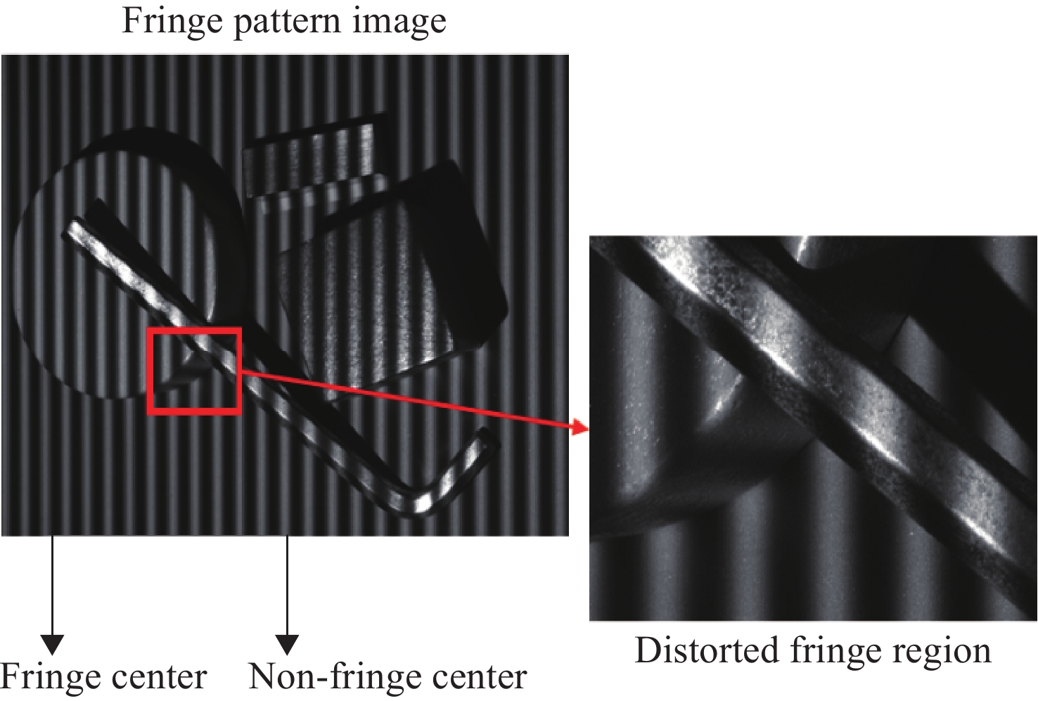
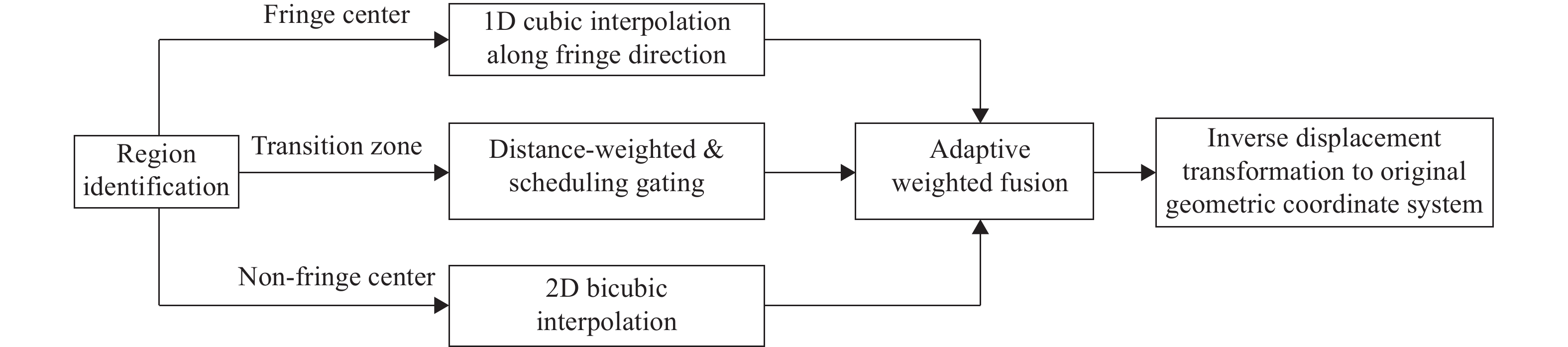
方法该方法在图像灰度域完成条纹超分辨,但利用相位域解算得到的载波强度指数、局部调制度和多频包裹相位作为物理约束。首先,利用归一化载波强度指数对条纹脊线、谷线及过渡区域进行结构解耦,并结合脊谷距离与局部调制度构建联合权重;随后,基于多频相移信息估计二维条纹对齐位移场,经局部相关细化与二维总变差正则化后,将原始条纹映射至条纹对齐域并实施方向性插值;最后,依据位移场梯度与局部相位变化率构建平坦区陡变区自适应融合策略,实现面向相位保真的条纹重采样与三维测量。
结果在3 mm、6 mm 和9 mm 量块实验中,所提方法将平均绝对误差由
0.0290 mm 降至0.0208 mm,均方根误差由0.0428 mm 降至0.0295 mm;在 PCB 引脚区域和晶振封装区域中,所提方法均改善了相位连续性和三维重建稳定性。以引脚区域为例,与图像双三次插值相比,所提方法将平均绝对误差由0.1753 mm降至0.0254 mm,降幅约为 85.5%。结论实验结果表明,该方法在当前 PCB 引脚区域和晶振封装局部结构中能够提高条纹重采样后的相位一致性和点云采样密度,并降低局部重建误差。
Abstract:Objective: This study addresses fringe-based three-dimensional measurement of local structures on complex reflective printed circuit boards. Uniform image interpolation may distort sinusoidal fringes. Curved fringes may also cause a mismatch between the interpolation direction and local iso-phase lines. Low-modulation regions may further amplify phase errors.Methods: A measurement-oriented phase-preserving fringe super-resolution resampling method is proposed. The super-resolution operation is performed in the gray-image domain. Phase-domain quantities are used as physical constraints. First, a normalized carrier intensity index is used to decouple fringe ridges, valleys, and transition regions. Ridge-valley distance and local modulation are then combined to construct a joint weight. Next, a two-dimensional fringe-alignment displacement field is estimated from multi-frequency phase-shifting data. The field is refined by local correlation and two-dimensional total-variation regularization. The original fringe images are then mapped into an aligned domain for directional interpolation. Finally, a flat/steep-region adaptive fusion strategy is constructed using the displacement-field gradient and local phase variation rate.Results: In the 3 mm, 6 mm, and 9 mm gauge-block experiments, the proposed method reduced the mean absolute error from
0.0290 mm to0.0208 mm. It also reduced the root mean square error from0.0428 mm to0.0295 mm. In the high-reflective PCB pin region and the crystal oscillator package region, the proposed method improved phase continuity and three-dimensional reconstruction stability. In the pin region, compared with image-domain bicubic interpolation, the proposed method reduced the mean absolute error from0.1753 mm to0.0254 mm, corresponding to a reduction of about 85.5%. The error standard deviation was reduced to0.0126 mm.Conclusion:The proposed method improves phase consistency after fringe resampling, increases point-cloud sampling density, and reduces local reconstruction errors in the selected PCB regions. This super-resolution process should be interpreted as sampling-grid densification and interpolation-induced phase-error reduction, rather than as exceeding the true lateral resolution limited by the optical system. The current conclusions are limited to the tested PCB local ROIs and imaging conditions. -

图 1 三维重建流程 括号中标明各模块的主要操作域
Figure 1. Flow chart of the proposed 3D reconstruction framework. The terms in parentheses indicate the main operation domain of each module
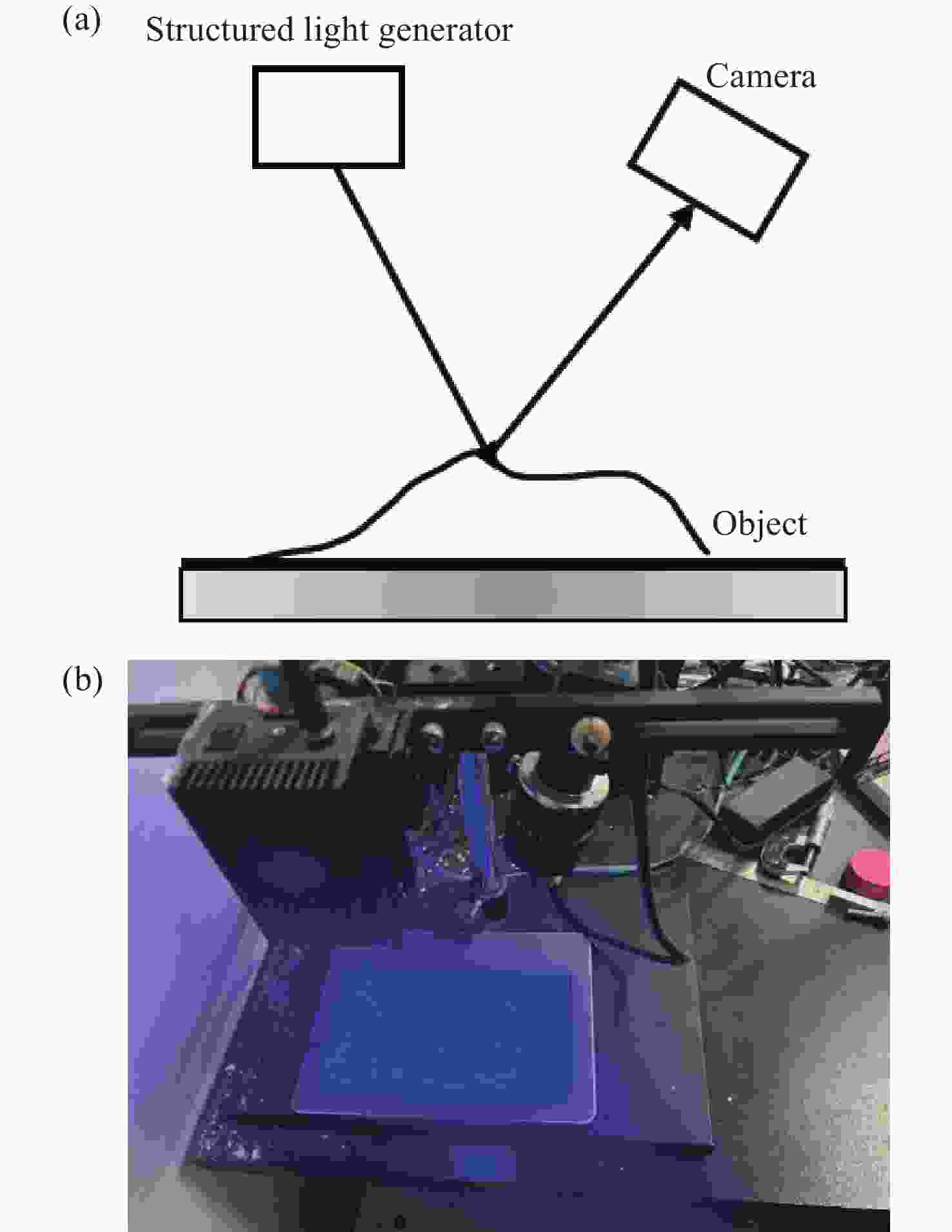
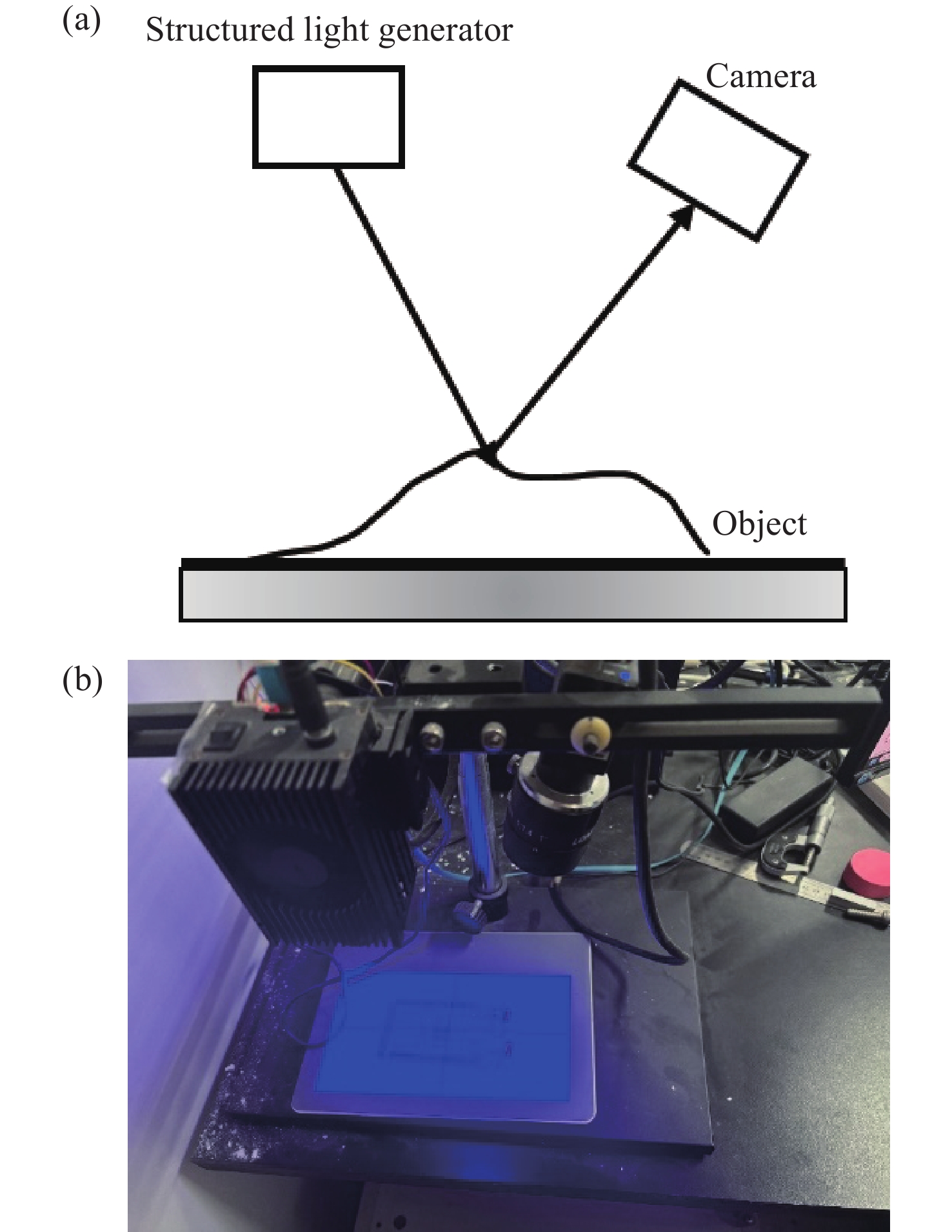
图 4 实验平台。((a)结构光系统示意图;(b)实验平台实物图)
Figure 4. Experimental setup. ((a) Structured light system; (b) photograph of the experimental platform)
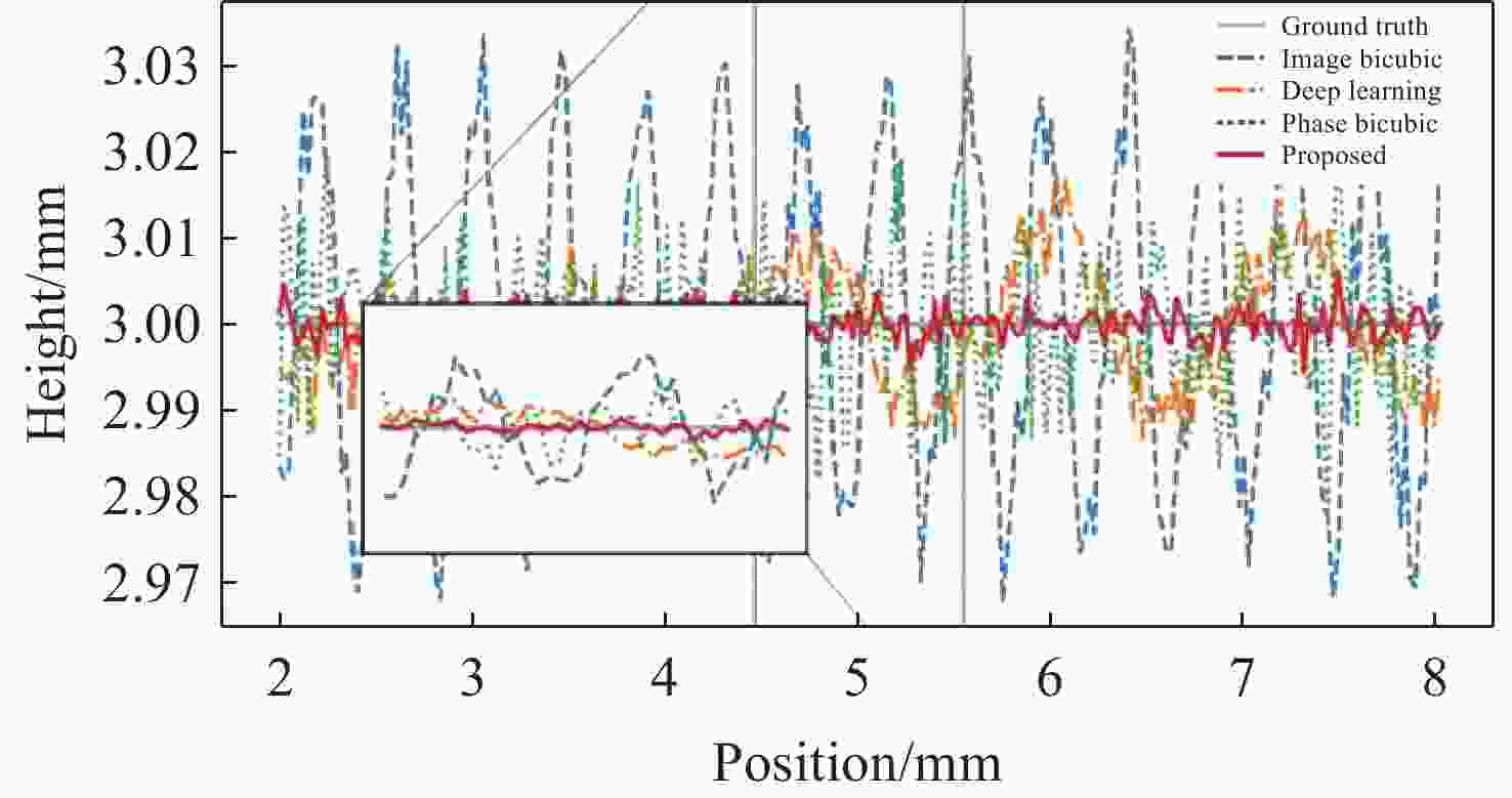
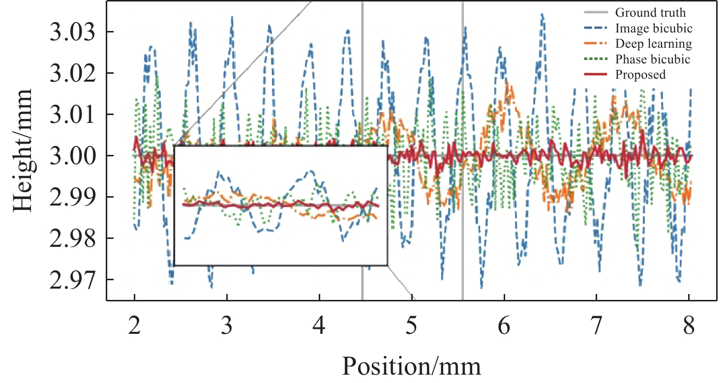
图 5 3mm标准量块的表面平面度剖面对比
Figure 5. Comparison of surface flatness profiles for a 3mm gauge block
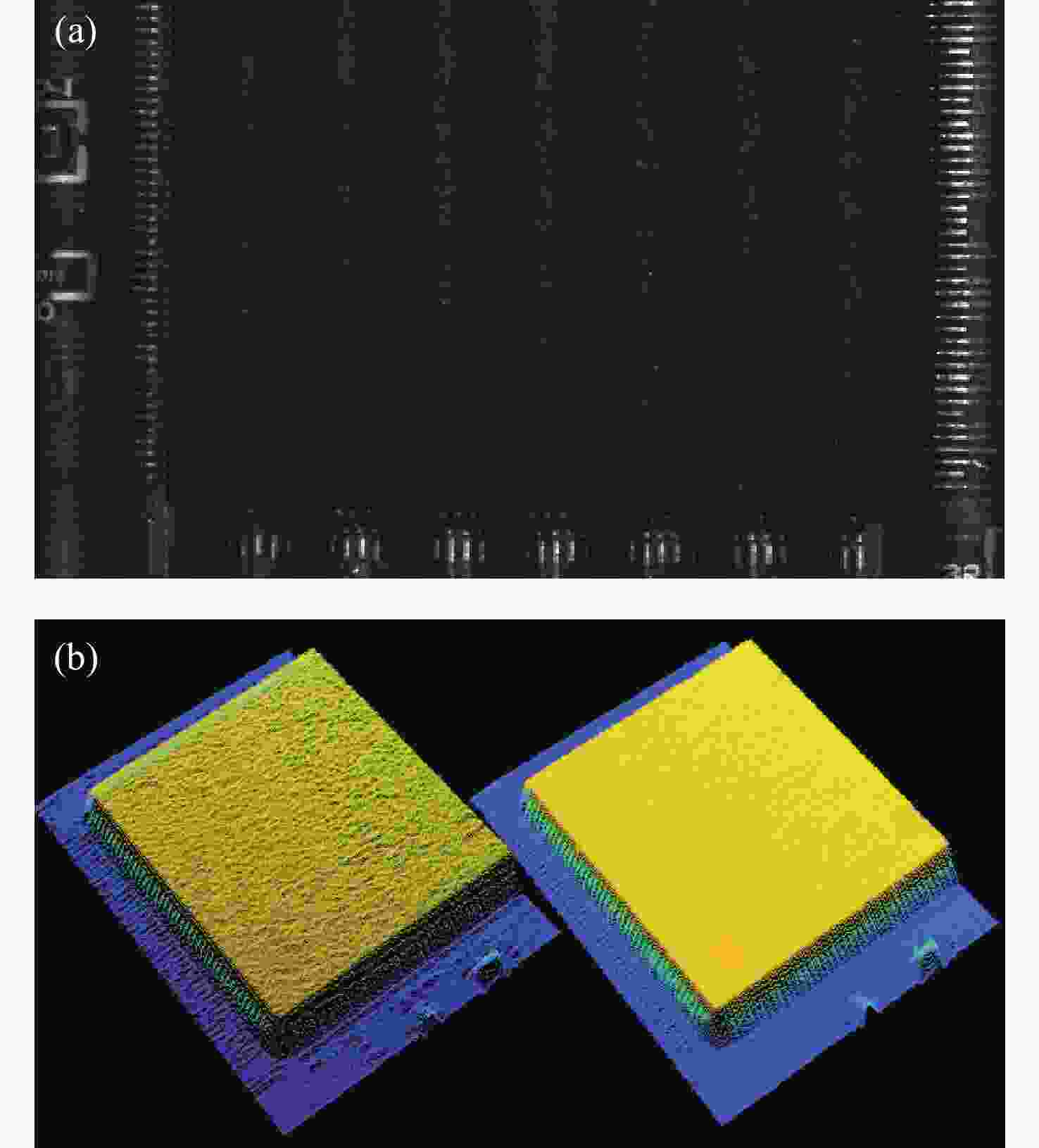
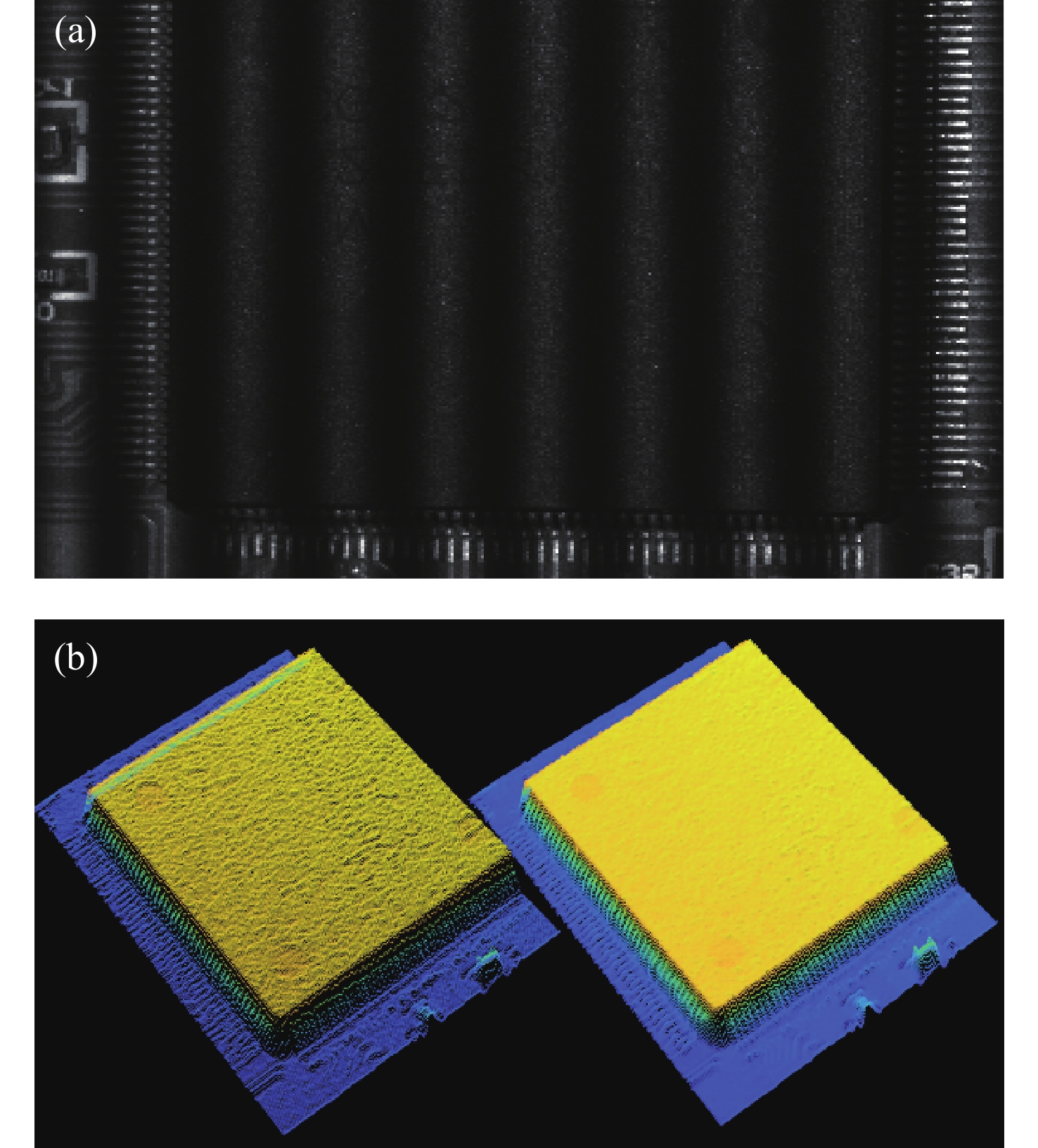
图 6 PCB表面重建效果对比((a)原始条纹图像(b)点云超分辨前后对比)
Figure 6. Comparison of PCB surface reconstruction results: (a) original fringe image; (b) point cloud before and after super-resolution
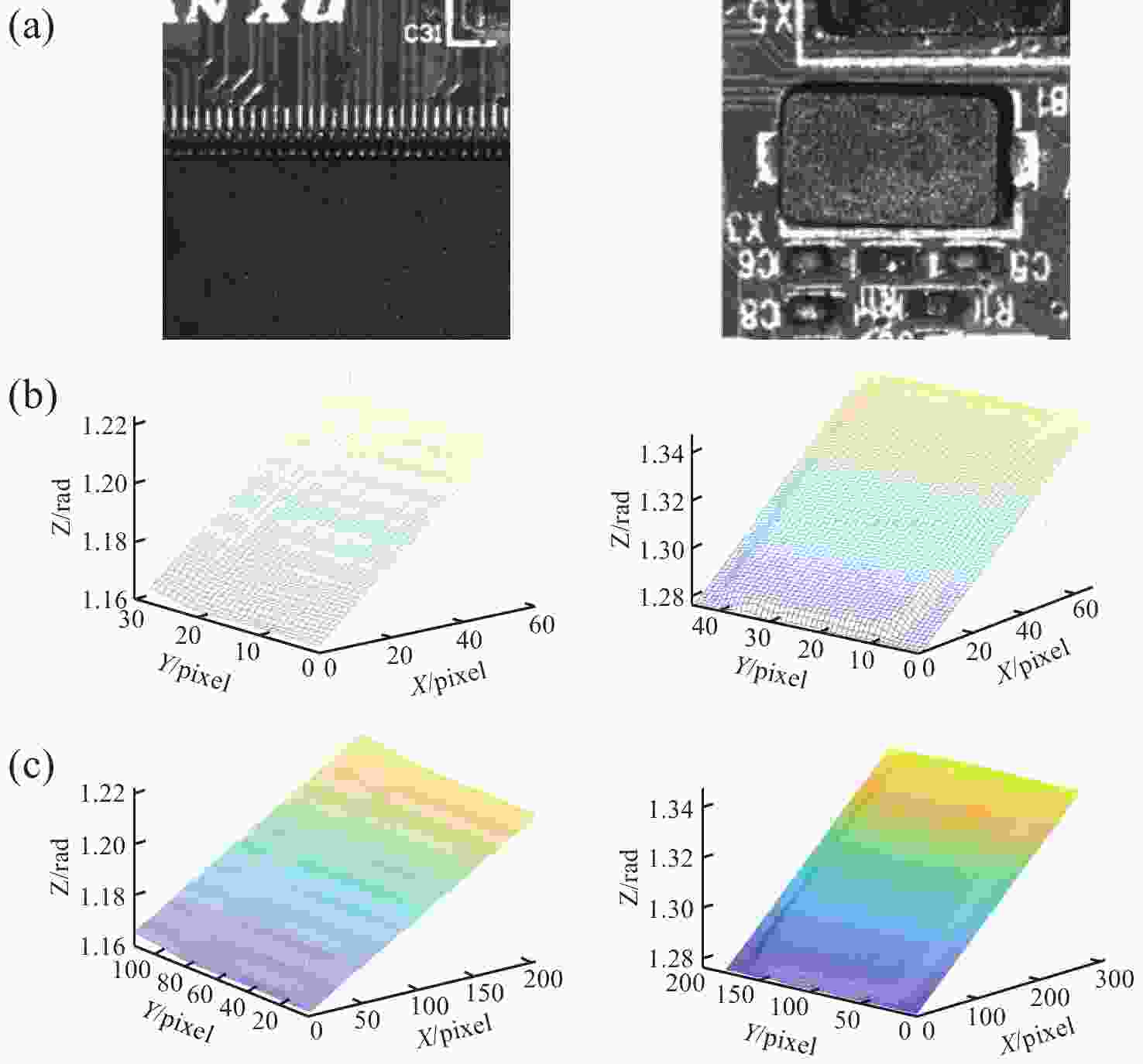
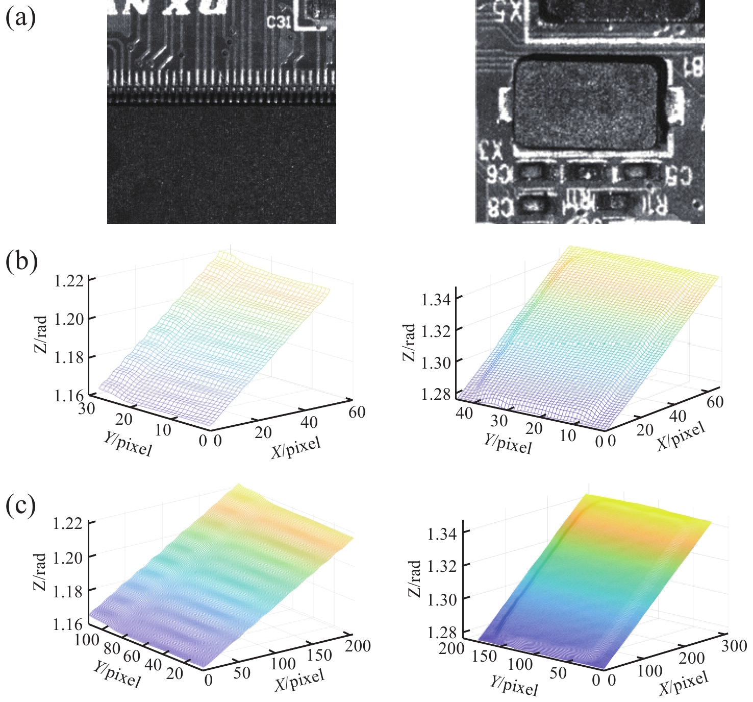
图 7 引脚区域与晶振封装区域的原始图像及相位结果对比。左列为高密度引脚区域,右列为晶振封装区域。(a)原始图像;(b)原始相位结果;(c)所提方法处理后的相位结果。
Figure 7. Comparison of original images and phase results in the pin region and crystal oscillator package region. The left column shows the high-density pin region, and the right column shows the crystal oscillator package region. (a) Original images; (b) original phase results; (c) phase results obtained by the proposed method.
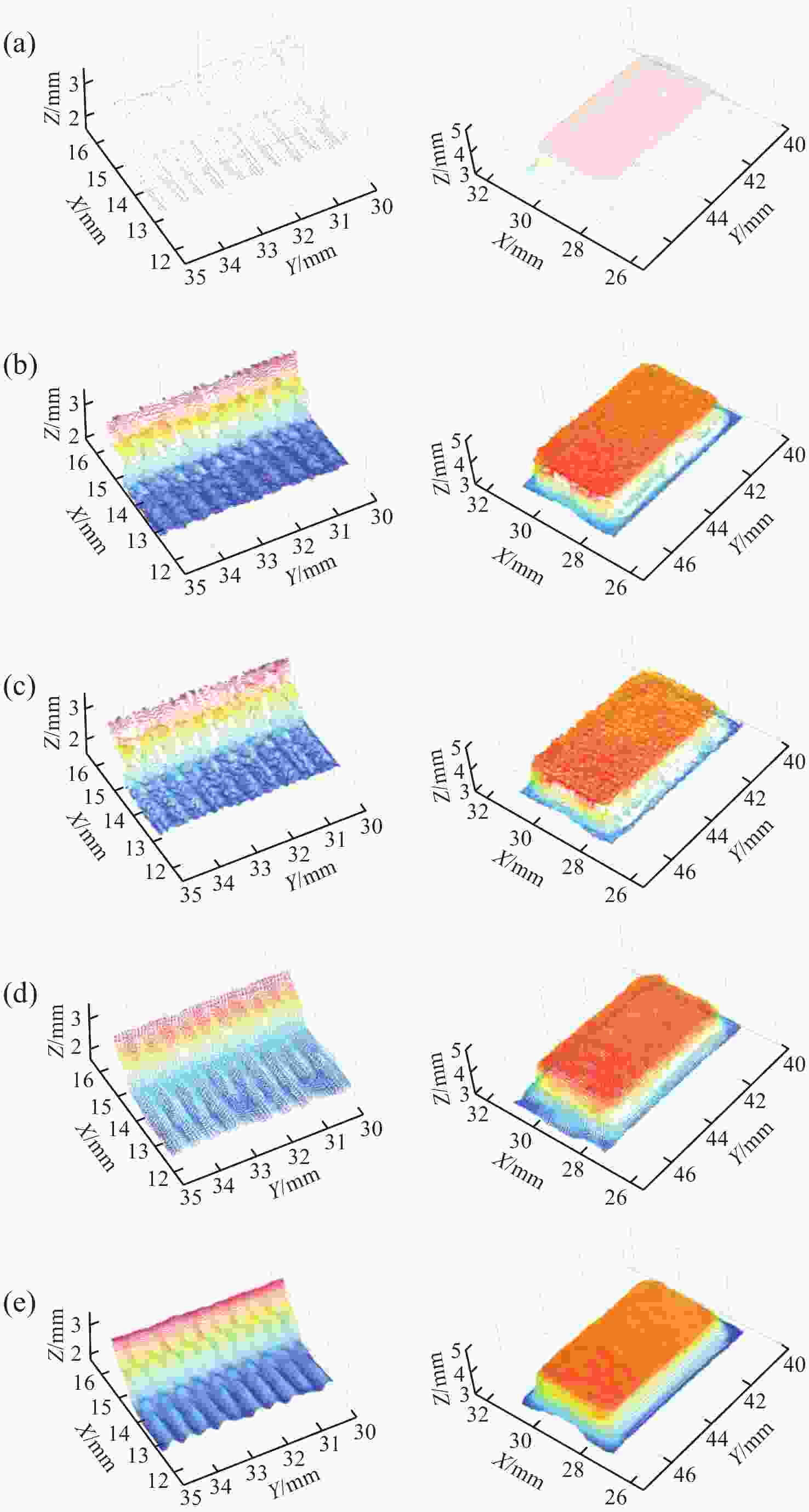
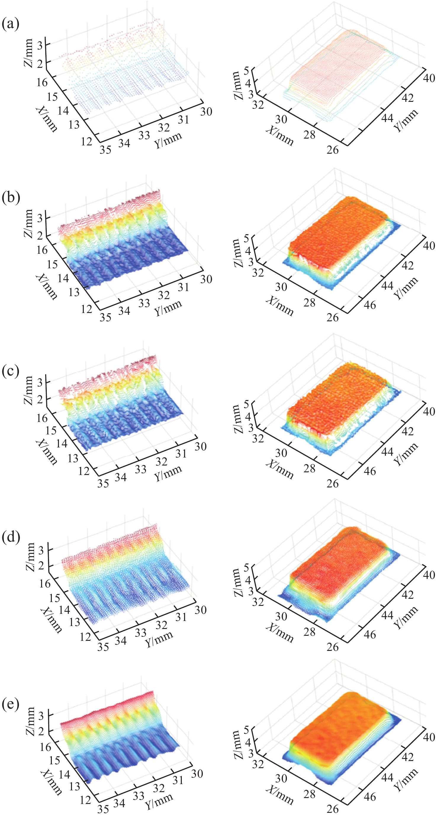
图 8 引脚区域与晶振封装区域的多方法三维重建结果对比。左列为高密度引脚区域,右列为晶振封装区域。(a)原始重建结果;(b)图像双三次插值结果;(c)基于深度学习的图像超分辨结果;(d)相位双三次插值结果;(e)所提方法的重建结果。
Figure 8. Comparison of 3D reconstruction results obtained by different methods in the pin region and crystal oscillator package region. The left column shows the high-density pin region, and the right column shows the crystal oscillator package region. (a) Original reconstruction; (b) image bicubic interpolation; (c) deep-learning-based image super-resolution; (d) phase bicubic interpolation ; (e) proposed method.
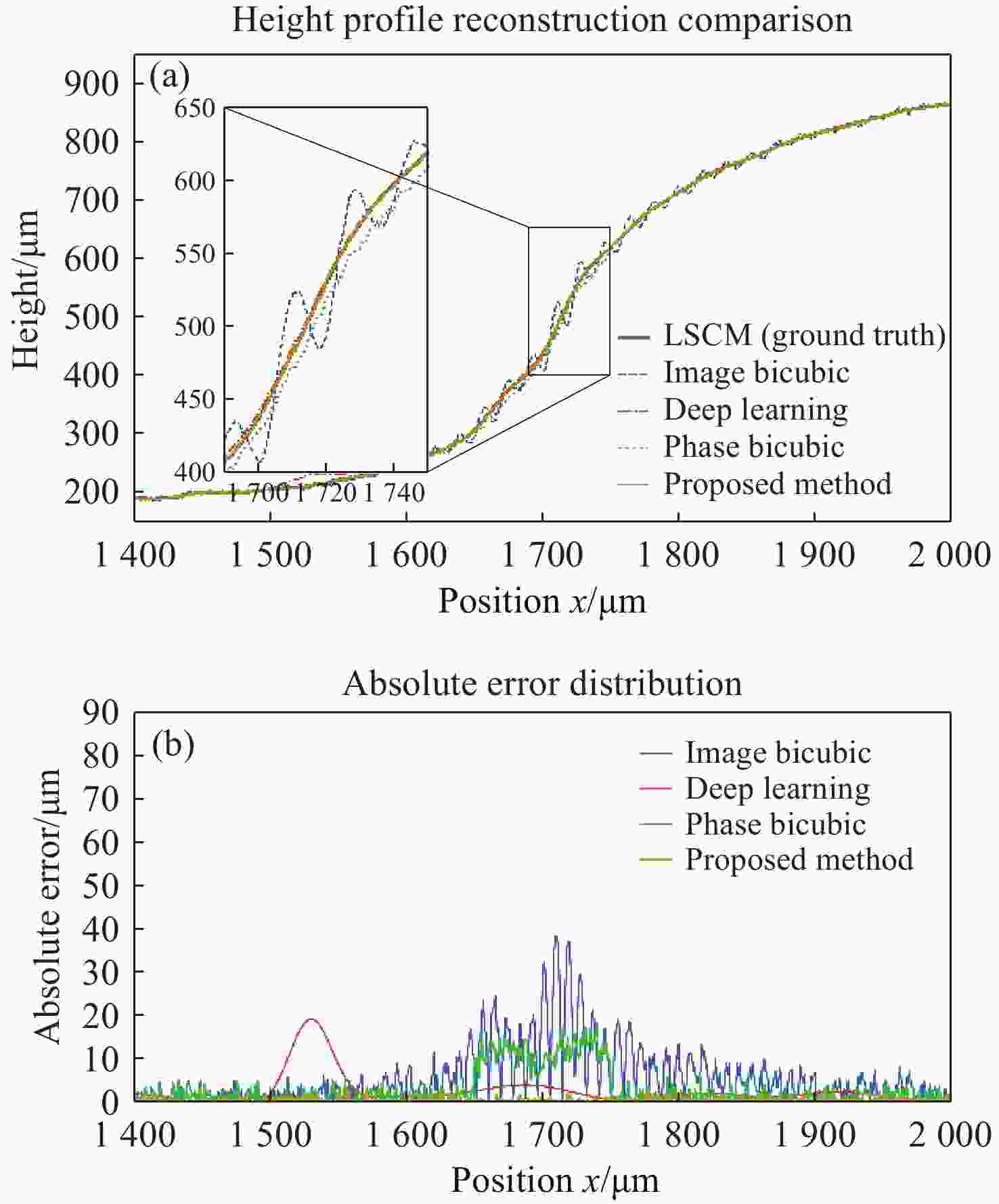
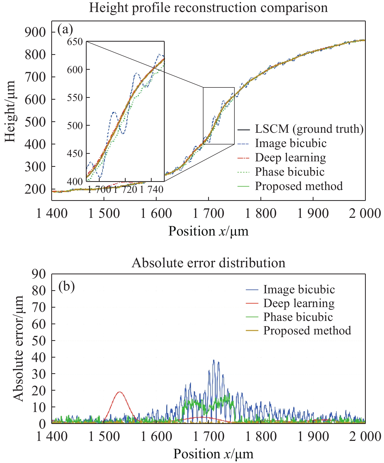
图 9 复杂PCB引脚表面的重建质量综合评估(a)高度截图轮廓对比(b)绝对重建误差分布
Figure 9. Comprehensive evaluation of reconstruction quality on a complex PCB pin surface: (a) height profile comparison; (b) absolute reconstruction error distribution
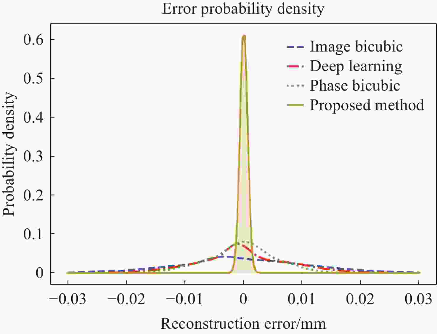
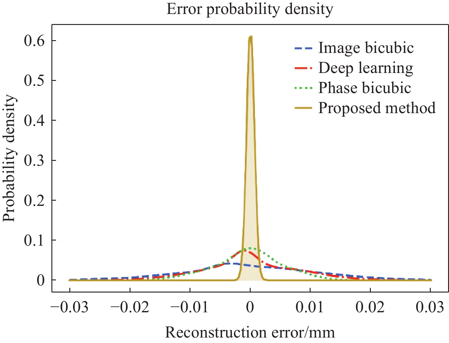
图 10 不同方法在 PCB 局部 ROI 内的绝对误差累积分布曲线
Figure 10. Cumulative distribution curves of absolute errors for different methods within the PCB local ROI.
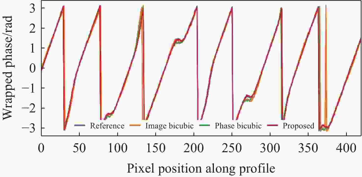
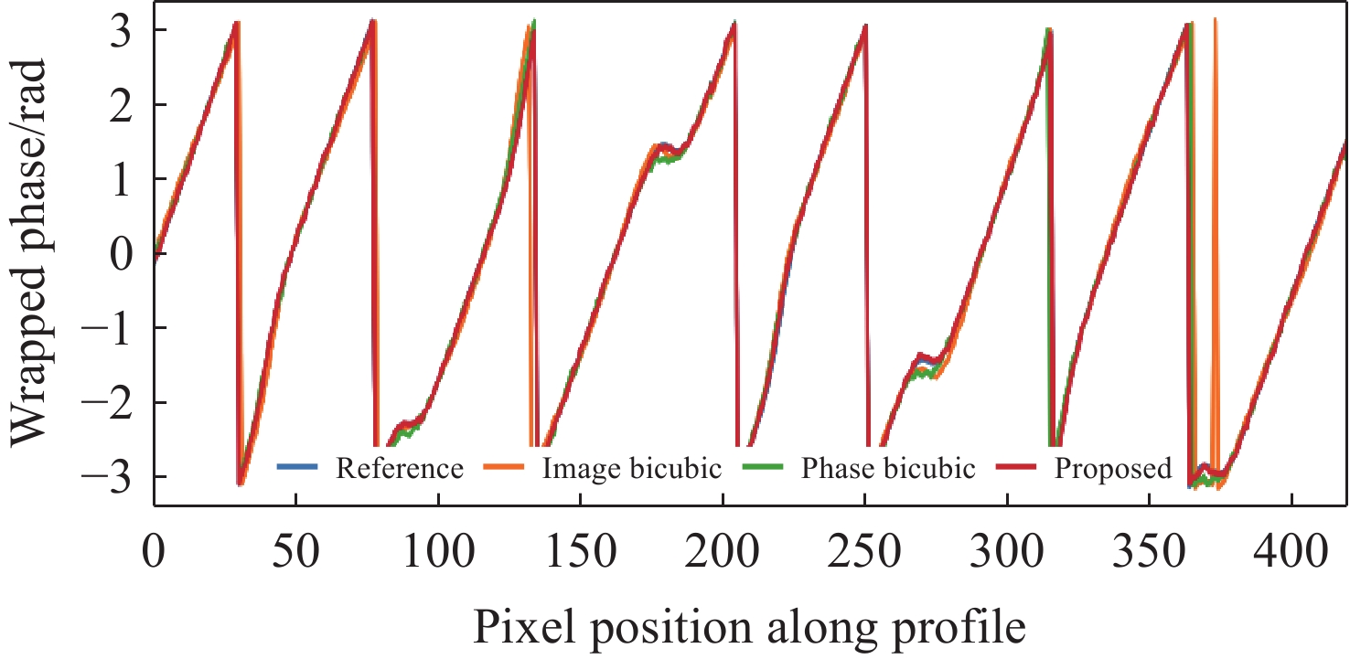
图 12 沿图11中标记剖面线提取的包裹相位曲线对比。
Figure 12. Comparison of wrapped-phase curves extracted along the marked profile line in Fig. 11.
表 1 不同方法主导计算代价对比
Table 1. Comparison of dominant computational costs among different methods
方法 时间复杂度 空间复杂度 依赖 双三次插值 O(R·C·t²) O(R·C·t²) CPU 样条插值 O(R·C·t²) O(R·C·t²) CPU 本文方法 O((N+F+$ {I}_{TV} $)·R·C + R·C·t²) O(R·C·t² + R·C) CPU 深度学习 O(k·R·C·t²), $ \mathrm{k}\gg 1 $ O(Model size + R·C·t²) GPU; 需预训练模型  下载: 导出CSV
表 6 主要误差指标的95%置信区间
Table 6. 95% confidence intervals of the main error metrics
实验场景 方法 >指标 均值 ± SD/mm 95% CI/mm 标准量块 原始重建 MAE 0.0290 ±0.0021 [ 0.0275 ,0.0305 ]本文方法 MAE 0.0208 ±0.0015 [ 0.0197 ,0.0219 ]原始重建 RMSE 0.0428 ±0.0037 [ 0.0402 ,0.0454 ]本文方法 RMSE 0.0295 ±0.0026 [ 0.0276 ,0.0314 ]引脚 图像双三次 MAE 0.1753 ±0.0120 [ 0.1667 ,0.1839 ]深度学习 MAE 0.1721 ±0.0140 [ 0.1621 ,0.1821 ]相位双三次 MAE 0.0485 ±0.0040 [ 0.0456 ,0.0514 ]本文方法 MAE 0.0254 ±0.0021 [ 0.0239 ,0.0269 ]本文方法 RMSE 0.0298 ±0.0026 [ 0.0279 ,0.0317 ]本文方法 MaxAE 0.0820 ±0.0110 [ 0.0741 ,0.0899 ]晶振 图像双三次 MAE 0.1626 ±0.0105 [ 0.1551 ,0.1701 ]深度学习 MAE 0.1667 ±0.0120 [ 0.1581 ,0.1753 ]相位双三次 MAE 0.0675 ±0.0055 [ 0.0636 ,0.0714 ]本文方法 MAE 0.0221 ±0.0018 [ 0.0208 ,0.0234 ]本文方法 RMSE 0.0347 ±0.0030 [ 0.0326 ,0.0368 ]本文方法 MaxAE 0.0950 ±0.0120 [ 0.0864 ,0.1036 ]
下载: 导出CSV
表 2 不同分辨率下测量结果对比
Table 2. Comparison of measurement results under different resolutions
量块 超分辨前 超分辨后 MAE/mm RMSE/mm MAE/mm RMSE/mm 3mm 0.0253 ±0.0018 0.0361 ±0.0032 0.0212 ±0.0015 **0.0226 ±0.0020 **6mm 0.0272 ±0.0020 0.0479 ±0.0041 0.0164 ±0.0012 **0.0332 ±0.0030 **9mm 0.0345 ±0.0026 0.0443 ±0.0038 0.0249 ±0.0019 **0.0326 ±0.0028 **平均 0.0290 ±0.0021 0.0428 ±0.0037 0.0208 ±0.0015 0.0295 ±0.0026
下载: 导出CSV
表 3 不同方法测量结果对比
Table 3. Comparison of measurement results by different methods
方法 RMSE/mm Planarity Error/mm 平均耗时/s 图像双三次 0.0497 ±0.0038 **0.0128 ±0.0011 **0.064 ± 0.004 深度学习 0.0482 ±0.0042 **0.0095 ±0.0009 **2.684 ± 0.100 相位双三次 0.0286 ±0.0023 **0.0078 ±0.0007 **0.071 ± 0.005 所提方法(无几何校正) 0.0395 ±0.0030 **0.0051 ±0.0005 *0.184 ± 0.012 所提方法(无权重融合) 0.0291 ±0.0024 **0.0073 ±0.0007 **0.263 ± 0.016 所提方法 0.0226 ±0.0018 0.0046 ±0.0004 0.342 ± 0.020
下载: 导出CSV
表 4 引脚区域与晶振封装区域不同方法的重建误差对比
Table 4. Reconstruction errors of different methods in the pin region and crystal oscillator package region
区域 方法 MAE/mm RMSE/mm STD/mm MaxAE/mm Planarity Error/mm 平均耗时/s 引脚 图像双三次 0.1753 ±0.0120 **0.2057 ±0.0160 **0.0951 ±0.0085 **0.560 ± 0.060** 0.0201 ±0.0020 **0.066 ± 0.005 深度学习 0.1721 ±0.0140 **0.2184 ±0.0180 **0.0758 ±0.0070 **0.590 ± 0.065** 0.0185 ±0.0018 **3.126 ± 0.130 相位双三次 0.0485 ±0.0040 **0.0552 ±0.0048 **0.0483 ±0.0042 **0.150 ± 0.020** 0.0123 ±0.0013 **0.074 ± 0.005 本文方法 0.0254 ±0.0021 0.0298 ±0.0026 0.0126 ±0.0014 0.082 ± 0.011 0.0081 ±0.0008 0.349 ± 0.020 晶振 图像双三次 0.1626 ±0.0105 **0.2416 ±0.0170 **0.1180 ±0.0100 **0.610 ± 0.070** 0.0220 ±0.0020 **0.068 ± 0.005 深度学习 0.1667 ±0.0120 **0.2447 ±0.0185 **0.1260 ±0.0110 **0.630 ± 0.075** 0.0292 ±0.0025 **3.184 ± 0.135 相位双三次 0.0675 ±0.0055 **0.1332 ±0.0120 **0.0815 ±0.0075 **0.310 ± 0.040** 0.0180 ±0.0016 0.079 ± 0.006 本文方法 0.0221 ±0.0018 0.0347 ±0.0030 0.0158 ±0.0016 0.095 ± 0.012 0.0176 ±0.0014 0.361 ± 0.022
下载: 导出CSV
表 5 不同方法在相位域中的定量比较
Table 5. Quantitative comparison of different methods in the phase domain
方法 phase MAE / rad phase RMSE / rad 相位误差 STD / rad 结果说明 图像双三次 0.092 0.124 0.083 边缘附近易出现局部振荡
与周期性扰动相位双三次 0.050 0.074 0.054 可减弱相位扰动,
但边缘存在过平滑本文方法 0.028 0.037 0.025 平坦区与边缘区均与参考
结果保持较高一致性
下载: 导出CSV
表 7 PCB 引脚区域不同图像扰动条件下的鲁棒性分析
Table 7. Robustness analysis under different image perturbation conditions in the PCB pin region
扰动类型 条件 图像双三次
MAE/mm相位双三次
MAE/mm本文方法
MAE/mm图像双三次
RMSE/mm相位双三次
RMSE/mm本文方法
RMSE/mm无扰动 Baseline 0.1753 ±0.0120 0.0485 ±0.0040 0.0254 ±0.0021 0.2057 ±0.0160 0.0552 ±0.0048 0.0298 ±0.0026 高斯噪声 σ = 0.01 0.1846 ±0.0134 0.0506 ±0.0044 0.0262 ±0.0024 0.2162 ±0.0176 0.0574 ±0.0052 0.0307 ±0.0029 σ = 0.02 0.1978 ±0.0152 0.0539 ±0.0049 0.0274 ±0.0028 0.2315 ±0.0195 0.0612 ±0.0059 0.0321 ±0.0032 σ = 0.04 0.2265 ±0.0196 0.0618 ±0.0058 0.0301 ±0.0034 0.2648 ±0.0240 0.0699 ±0.0068 0.0351 ±0.0040 曝光扰动 α = 0.7 0.2072 ±0.0165 0.0556 ±0.0051 0.0279 ±0.0029 0.2436 ±0.0210 0.0637 ±0.0060 0.0329 ±0.0034 α = 1.3 0.1991 ±0.0158 0.0542 ±0.0048 0.0275 ±0.0028 0.2338 ±0.0202 0.0621 ±0.0058 0.0324 ±0.0033 α = 1.5 0.2348 ±0.0215 0.0639 ±0.0063 0.0309 ±0.0036 0.2764 ±0.0265 0.0728 ±0.0075 0.0362 ±0.0042
下载: 导出CSV
-
[1] YU J B, ZHAO L X, WANG Y SH, et al. Defect detection of printed circuit board based on adaptive key-points localization network[J]. Computers & Industrial Engineering, 2024, 193: 110258. doi: 10.1016/j.cie.2024.110258 [2] FUNG K C, XUE K W, LAI C M, et al. Improving PCB defect detection using selective feature attention and pixel shuffle pyramid[J]. Results in Engineering, 2024, 21: 101992. doi: 10.1016/j.rineng.2024.101992 [3] ZHOU Y B, YUAN M H, ZHANG J, et al. Review of vision-based defect detection research and its perspectives for printed circuit board[J]. Journal of Manufacturing Systems, 2023, 70: 557-578. doi: 10.1016/j.jmsy.2023.08.019 [4] 朱黎颖, 王森, 沈爱萍, 等. 复杂背景下的电路板表面焊接缺陷视觉检测[J]. 光学 精密工程, 2024, 32(14): 2256-2271. doi: 10.37188/OPE.20243214.2256ZHU L Y, WANG S, SHEN A P, et al. Visual inspection of soldering defects on board surfaces against complex backgrounds[J]. Optics and Precision Engineering, 2024, 32(14): 2256-2271. (in Chinese). doi: 10.37188/OPE.20243214.2256 [5] YANG J, LIU ZH X, DU W N, et al. A PCB defect detector based on coordinate feature refinement[J]. IEEE Transactions on Instrumentation and Measurement, 2023, 72: 5029410. doi: 10.1109/tim.2023.3322483 [6] GUO Y L, WANG H Y, HU Q Y, et al. Deep learning for 3D point clouds: a survey[J]. IEEE Transactions on Pattern Analysis and Machine Intelligence, 2021, 43(12): 4338-4364. doi: 10.1109/TPAMI.2020.3005434 [7] ZUO CH, QIAN J M, FENG SH J, et al. Deep learning in optical metrology: a review[J]. Light: Science & Applications, 2022, 11(1): 39. [8] LAGA H, JOSPIN L V, BOUSSAID F, et al. A survey on deep learning techniques for stereo-based depth estimation[J]. IEEE Transactions on Pattern Analysis and Machine Intelligence, 2022, 44(4): 1738-1764. doi: 10.1109/TPAMI.2020.3032602 [9] WANG D, LIU ZH, SHAO SH W, et al. Monocular depth estimation: a survey[C]. IECON 2023- 49th Annual Conference of the IEEE Industrial Electronics Society, IEEE, 2023: 1-7. [10] CHOI H, MAY N, PHOULADY A, et al. Rapid three-dimensional reconstruction of printed circuit board using femtosecond laser delayering and digital microscopy[J]. Microelectronics Reliability, 2022, 138: 114659. doi: 10.1016/j.microrel.2022.114659 [11] 刘飞, 罗惠方, 江翰立, 等. 改进的三频三步相移结构光三维重建方法[J]. 红外与激光工程, 2022, 51(4): 20210179. doi: 10.3788/IRLA20210179LIU F, LUO H F, JIANG H L, et al. Modified three-dimensional reconstruction based on three-frequency three-step phase shifting algorithm[J]. Infrared and Laser Engineering, 2022, 51(4): 20210179. (in Chinese). doi: 10.3788/IRLA20210179 [12] YANG D, QIAO D Y, XIA CH F, et al. Adaptive horizontal scaling method for speckle-assisted fringe projection profilometry[J]. Optics Express, 2023, 31(1): 328-343. doi: 10.1364/OE.478078 [13] LYU C Y, LI P, WANG D CH, et al. High-speed optical 3D measurement sensor for industrial application[J]. IEEE Sensors Journal, 2021, 21(10): 11253-11261. doi: 10.1109/JSEN.2020.3006566 [14] RANFTL R, BOCHKOVSKIY A, KOLTUN V. Vision transformers for dense prediction[C]. 2021 IEEE/CVF International Conference on Computer Vision (ICCV), IEEE, 2021: 12179-12188. [15] CAO Y L, DING B J, HE Z W, et al. Learning inter- and intraframe representations for non-Lambertian photometric stereo[J]. Optics and Lasers in Engineering, 2022, 150: 106838. doi: 10.1016/j.optlaseng.2021.106838 [16] 王腾, 杨树明, 李述胜, 等. 振镜激光扫描测量系统误差分析与补偿[J]. 光学学报, 2020, 40(23): 2315001. doi: 10.3788/AOS202040.2315001WANG T, YANG SH M, LI SH SH, et al. Error analysis and compensation of galvanometer laser scanning measurement system[J]. Acta Optica Sinica, 2020, 40(23): 2315001. (in Chinese). doi: 10.3788/AOS202040.2315001 [17] PARE A, ZHANG SH F, LEI ZH CH. Multipath interference suppression in time-of-flight sensors by exploiting the amplitude envelope of the transmission signal[J]. IEEE Access, 2020, 8: 167527-167536. doi: 10.1109/ACCESS.2020.3023083 [18] HU Y, CHEN Q, FENG SH J, et al. Microscopic fringe projection profilometry: a review[J]. Optics and Lasers in Engineering, 2020, 135: 106192. doi: 10.1016/j.optlaseng.2020.106192 [19] 吴周杰, 张启灿. 基于条纹投影的三维形貌与形变测量技术研究进展[J]. 液晶与显示, 2023, 38(6): 730-747. doi: 10.37188/CJLCD.2023-0082WU ZH J, ZHANG Q C. Recent progress on 3D shape and deformation measurement based on fringe projection[J]. Chinese Journal of Liquid Crystals and Displays, 2023, 38(6): 730-747. (in Chinese). doi: 10.37188/CJLCD.2023-0082 [20] LY SH ZH, KEMAO Q. Modeling the measurement precision of fringe projection profilometry[J]. Light: Science & Applications, 2023, 12(1): 257. [21] ZUO CH, FENG SH J, HUANG L, et al. Phase shifting algorithms for fringe projection profilometry: a review[J]. Optics and Lasers in Engineering, 2018, 109: 23-59. doi: 10.1016/j.optlaseng.2018.04.019 [22] FENG SH J, ZUO CH, ZHANG L, et al. Calibration of fringe projection profilometry: a comparative review[J]. Optics and Lasers in Engineering, 2021, 143: 106622. doi: 10.1016/j.optlaseng.2021.106622 [23] JUAREZ-SALAZAR R, RODRIGUEZ-REVELES G A, ESQUIVEL-HERNANDEZ S, et al. Three-dimensional spatial point computation in fringe projection profilometry[J]. Optics and Lasers in Engineering, 2023, 164: 107482. doi: 10.1016/j.optlaseng.2023.107482 [24] BOUKHTACHE S, BLAYSAT B, GRÉDIAC M, et al. Alternatives to bicubic interpolation considering FPGA hardware resource consumption[J]. IEEE Transactions on Very Large Scale Integration (VLSI) Systems, 2021, 29(2): 247-258. doi: 10.1109/TVLSI.2020.3032888 [25] LIANG J Y, CAO J ZH, SUN G L, et al. SwinIR: image restoration using Swin transformer[C]. 2021 IEEE/CVF International Conference on Computer Vision Workshops (ICCVW), IEEE, 2021: 1833-1844. -

 下载:
下载:


计量
- 文章访问数: 3
- HTML全文浏览量: 2
- PDF下载量: 0
- 被引次数: 0
