



Study onnanoscale etching of silicon carbide for deep-subwavelength features based on spatiotemporally shaped ultrafast laser pulses
-
摘要:
飞秒激光自组干涉协同近场增强效应和孵化效应能够实现深亚波长纳米刻蚀,然而其结构形成通常依赖表面随机散射中心以及多脉冲反馈,存在一致性差、重复性差、激光参数敏感等问题。本文提出时空协同的激光能量调控策略,以提升4H-SiC单晶表面纳米槽刻写质量。在空间域,采用单狭缝和双狭缝光束整形重构焦平面能量分布,抑制能量横向扩散,增强孵化效应和自组干涉效应;在时间域,引入GHz脉冲串调控能量注入时序,降低瞬时能量沉积强度并延长退火时间。通过静态定点辐照与动态扫描实验,系统探究不同调控手段下的表面形貌演化规律及纳米槽成形机制。结果表明,单狭缝整形后的椭圆焦斑可增强孵化效应和弱退火作用,获得一致性与边缘规整的62 nm最窄槽宽;双狭缝整形进一步增强了干涉场约束效应,降低了纳米槽成形对随机散射中心的依赖,将最小可控槽宽压缩至34 nm;在双狭缝整形基础上引入GHz脉冲串,400 ps间隔子脉冲的分步能量注入可降低瞬时强激发并抑制重熔堆积物和颗粒附着,使纳米槽最小可控槽宽进一步降低至24.5 nm。时空协同调控策略为第三代半导体表面高精度、低损伤、高重复性的纳米制造提供了有效技术方案与理论依据。
Abstract:Femtosecond-laser-induced self-organized interference, together with near-field enhancement and incubation effects, enables deep-subwavelength nanoetching. However, the formation of such structures usually relies on random surface scattering centers and multi-pulse feedback, leading to poor uniformity, limited repeatability, and high sensitivity to laser parameters. In this work, a spatiotemporal laser-energy modulation strategy is proposed to improve the writing quality of nanogrooves on 4H-SiC single-crystal surfaces. In the spatial domain, single-slit and double-slit beam shaping are employed to reconstruct the focal-plane energy distribution, suppress lateral energy spreading, and enhance the incubation and self-organized interference effects. In the temporal domain, a GHz burst mode is introduced to regulate the energy-deposition sequence, reduce the instantaneous energy-deposition intensity, and extend the annealing time. Static irradiation and dynamic scanning experiments were conducted to systematically investigate the surface morphology evolution and nanogroove formation mechanism under different modulation strategies. The results show that the elliptical focal spot formed by single-slit shaping enhances the incubation and annealing effects, producing nanogrooves with improved uniformity and edge regularity and a minimum groove width of 62 nm. Double-slit shaping further strengthens the interference-field confinement, reduces the dependence of nanogroove formation on random scattering centers, and decreases the minimum controllable groove width to 34 nm. By introducing GHz burst pulses on the basis of double-slit shaping, stepwise energy deposition through sub-pulses with a 400 ps interval reduces instantaneous strong excitation and suppresses molten redeposition and particle attachment, further decreasing the minimum controllable groove width to 24.5 nm. This spatiotemporal modulation strategy provides an effective technical approach and theoretical basis for high-precision, low-damage, and highly repeatable nanomanufacturing on third-generation semiconductor surfaces.
-
Key words:
- ultrafast laser nanofabrication /
- silicon carbide /
- slit beam shaping /
- burst mode /
- nanogroove
-
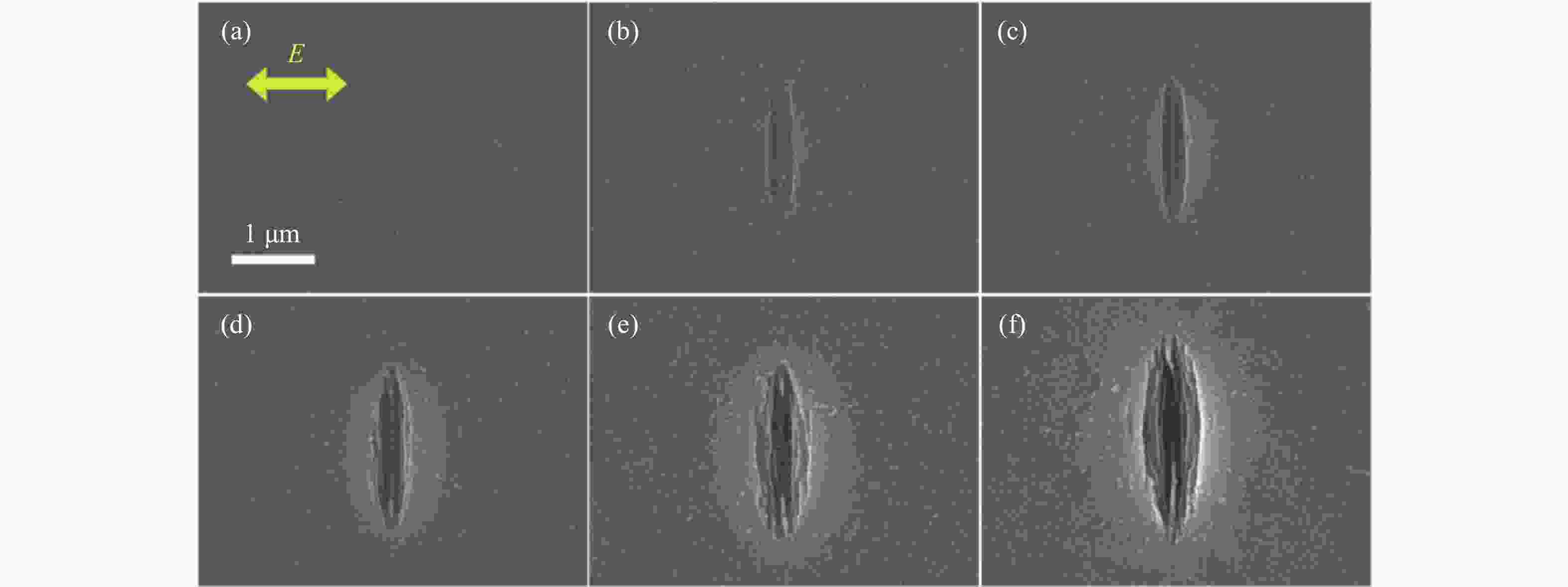
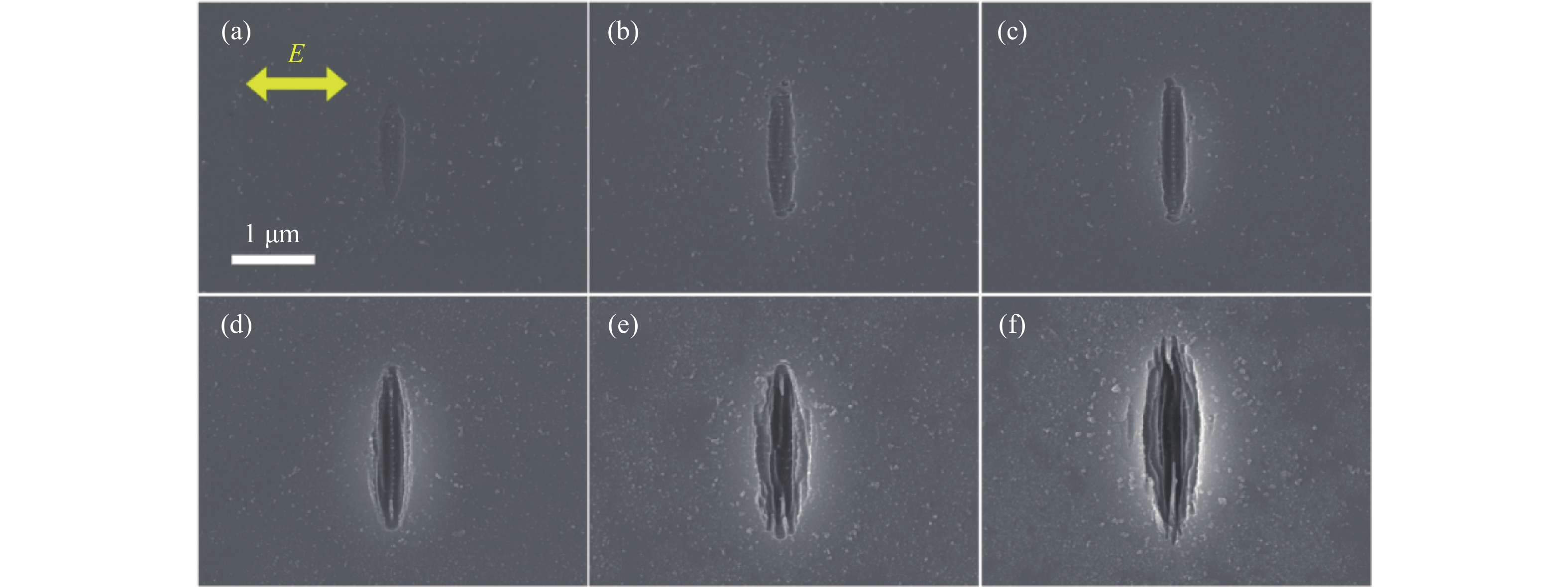
图 1 单脉冲能量13 nJ,不同脉冲数,微结构的演化过程,图(a)至图(f)脉冲数依次是4、6、8、10、12、14
Figure 1. Evolution of microstructures on the upper surface of SiC under a single-pulse energy of 13 nJ: (a) 4, (b) 6, (c) 8, (d) 10, (e) 12, and (f) 14.

图 2 (a)纳米槽3D形貌示意图;(b)纳米槽形貌SEM图;(c)纳米槽截面形貌SEM图
Figure 2. (a) Schematic of 3D morphology of nanogroove; (b) SEM image of nanogroove morphology; (c) SEM image of cross-sectional morphology.
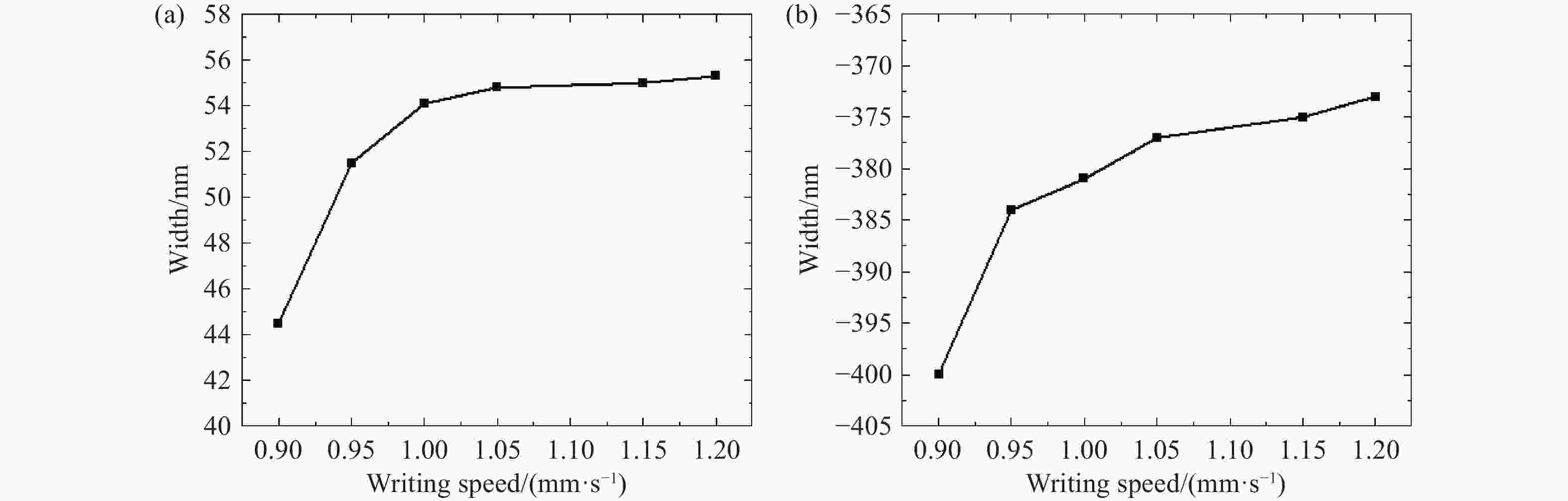
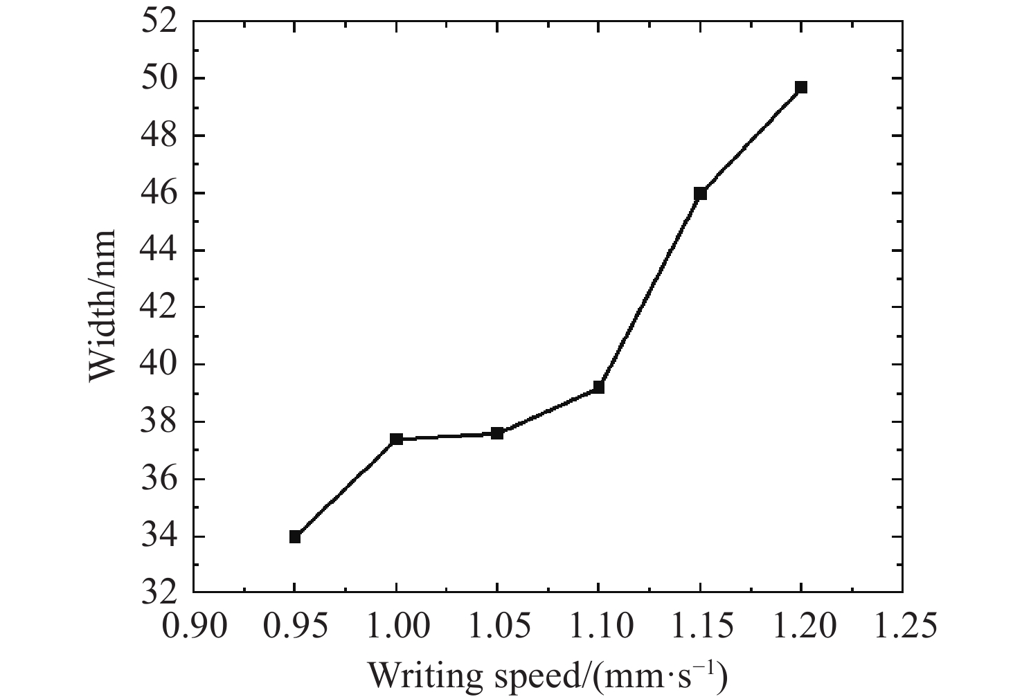
图 3 单脉冲能量19 nJ下,不同加工速度纳米槽(a)宽度和(b)深度的变化趋势
Figure 3. Trends in (a) width and (b) depth of nanogrooves with different processing speeds under a single-pulse energy of 19 nJ.
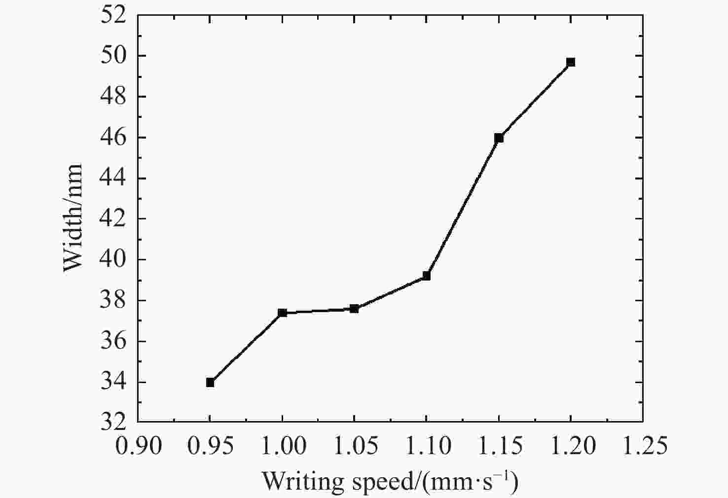
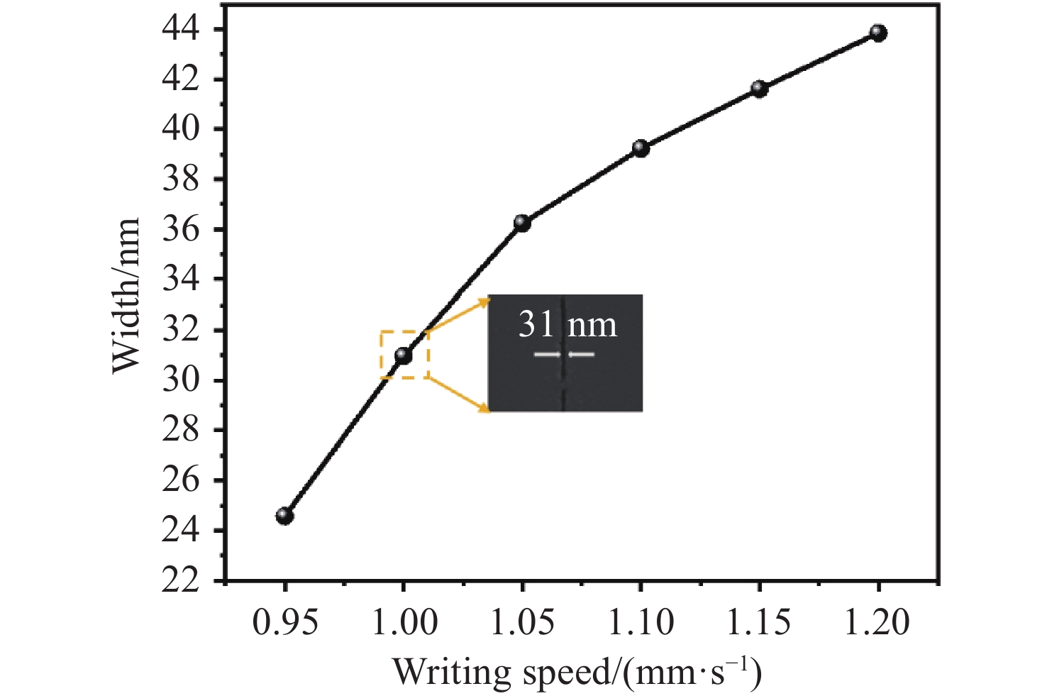
图 4 双狭缝整形后,不同加工速度纳米槽宽度变化趋势
Figure 4. Trends in nanogroove width with different processing speeds after double-slit shaping.

图 5 GHz脉冲串能量6 nJ,不同脉冲串个数,微结构的演化过程,图(a)至图(c)脉冲串个数分别是4、6、10
Figure 5. Evolution of microstructures under GHz burst irradiation with a burst energy of 6 nJ. Panels (a)–(c) correspond to burst numbers: (a) 4, (b) 6, and (c) 10.
-
[1] BERESNA M, KAZANSKY P G. Polarization diffraction grating produced by femtosecond laser nanostructuring in glass[J]. Optics Letters, 2010, 35(10): 1662-1664. doi: 10.1364/OL.35.001662 [2] BERESNA M, GECEVIČIUS M, KAZANSKY P G. Polarization sensitive elements fabricated by femtosecond laser nanostructuring of glass [Invited][J]. Optical Materials Express, 2011, 1(4): 783-795. doi: 10.1364/OME.1.000783 [3] DREVINSKAS R, KAZANSKY P G. High-performance geometric phase elements in silica glass[J]. APL Photonics, 2017, 2(6): 066104. doi: 10.1063/1.4984066 [4] DREVINSKAS R, BERESNA M, ZHANG J Y, et al. Ultrafast laser‐induced metasurfaces for geometric phase manipulation[J]. Advanced Optical Materials, 2017, 5(1): 1600575. doi: 10.1002/adom.201600575 [5] MINGAREEV I, HORN A. Time-resolved investigations of plasma and melt ejections in metals by pump-probe shadowgrpahy[J]. Applied Physics A, 2008, 92(4): 917-920. doi: 10.1007/s00339-008-4562-7 [6] PHILLIPS K C, GANDHI H H, MAZUR E, et al. Ultrafast laser processing of materials: a review[J]. Advances in Optics and Photonics, 2015, 7(4): 684-712. doi: 10.1364/AOP.7.000684 [7] SIPE J E, YOUNG J F, PRESTON J S, et al. Laser-induced periodic surface structure. I. Theory[J]. Physical Review B, 1983, 27(2): 1141-1154. doi: 10.1103/PhysRevB.27.1141 [8] MIYAJI G, MIYAZAKI K. Origin of periodicity in nanostructuring on thin film surfaces ablated with femtosecond laser pulses[J]. Optics Express, 2008, 16(20): 16265-16271. doi: 10.1364/OE.16.016265 [9] BONSE J, KRÜGER J, HÖHM S, et al. Femtosecond laser-induced periodic surface structures[J]. Journal of Laser Applications, 2012, 24(4): 042006. doi: 10.2351/1.4712658 [10] BIRNBAUM M. Semiconductor surface damage produced by ruby lasers[J]. Journal of Applied Physics, 1965, 36(11): 3688-3689. doi: 10.1063/1.1703071 [11] SHIMOTSUMA Y, KAZANSKY P G, QIU J R, et al. Self-organized nanogratings in glass irradiated by ultrashort light pulses[J]. Physical Review Letters, 2003, 91(24): 247405. doi: 10.1103/PhysRevLett.91.247405 [12] BHARDWAJ V R, SIMOVA E, RAJEEV P P, et al. Optically produced arrays of planar nanostructures inside fused silica[J]. Physical Review Letters, 2006, 96(5): 057404. doi: 10.1103/PhysRevLett.96.057404 [13] TAYLOR R, HNATOVSKY C, SIMOVA E. Applications of femtosecond laser induced self-organized planar nanocracks inside fused silica glass[J]. Laser & Photonics Reviews, 2008, 2(1-2): 26-46. doi: 10.1002/lpor.200710031 [14] LI ZH Z, WANG L, FAN H, et al. O-FIB: far-field-induced near-field breakdown for direct nanowriting in an atmospheric environment[J]. Light: Science & Applications, 2020, 9(1): 41. [15] ZHANG G D, RUDENKO A, STOIAN R, et al. Ultrafast laser high-aspect-ratio extreme nanostructuring of glass beyond λ/100[J]. Ultrafast Science, 2025, 5: 0103. doi: 10.34133/ultrafastscience.0103 [16] CHANAL M, FEDOROV V Y, CHAMBONNEAU M, et al. Crossing the threshold of ultrafast laser writing in bulk silicon[J]. Nature Communications, 2017, 8(1): 773. doi: 10.1038/s41467-017-00907-8 [17] WANG A D, DAS A, GROJO D. Ultrafast laser writing deep inside silicon with THz-repetition-rate trains of pulses[J]. Research, 2020, 2020: 8149764. doi: 10.34133/2020/8149764 [18] LIU M T, LU B L, LV J, et al. Polarization-dependent anisotropy of LIPSSs’ morphology evolution on a single-crystal silicon surface[J]. Micromachines, 2024, 15(2): 200. doi: 10.3390/mi15020200 [19] GUO X, PENG Z Y, DING P B, et al. Nonlinear optical properties of 6H-SiC and 4H-SiC in an extensive spectral range[J]. Optical Materials Express, 2021, 11(4): 1080-1092. doi: 10.1364/OME.415915 [20] REITANO R, BAERI P. Excimer laser induced thermal evaporation and ablation of silicon carbide[J]. Nuclear Instruments and Methods in Physics Research Section B: Beam Interactions with Materials and Atoms, 1996, 116(1-4): 369-372. doi: 10.1016/b978-0-444-82412-7.50055-9 [21] ZHANG R, HUANG CH ZH, WANG J, et al. Micromachining of 4H-SiC using femtosecond laser[J]. Ceramics International, 2018, 44(15): 17775-17783. doi: 10.1016/j.ceramint.2018.06.245 [22] OBARA G, SHIMIZU H, ENAMI T, et al. Growth of high spatial frequency periodic ripple structures on SiC crystal surfaces irradiated with successive femtosecond laser pulses[J]. Optics Express, 2013, 21(22): 26323-26334. doi: 10.1364/OE.21.026323 [23] NAN L, MANCINI A, WEBER T, et al. Angular dispersion suppression in deeply subwavelength phonon polariton bound states in the continuum metasurfaces[J]. Nature Photonics, 2025, 19(6): 615-623. doi: 10.1038/s41566-025-01670-9 [24] LIN ZH Y, LIU H G, JI L F, et al. Realization of ~ 10 nm features on semiconductor surfaces via femtosecond laser direct patterning in far field and in ambient air[J]. Nano Letters, 2020, 20(7): 4947-4952. doi: 10.1021/acs.nanolett.0c01013 [25] ZHANG Y CH, JIANG Q L, CAO K Q, et al. Extremely regular periodic surface structures in a large area efficiently induced on silicon by temporally shaped femtosecond laser[J]. Photonics Research, 2021, 9(5): 839-847. doi: 10.1364/PRJ.418937 [26] LONG M Q, HAN R ZH, CAO K Q, et al. High-quality diffractive optical elements on sapphire efficiently processed using shaped femtosecond laser[J]. Photonics Research, 2026, 14(4): 1299-1313. doi: 10.1364/PRJ.576398 [27] LI K, HAN R ZH, SUO M Q, et al. High quality nanogratings far beyond diffraction limits on silicon efficiently fabricated using femtosecond laser dual-beam interference direct writing[J]. Optics & Laser Technology, 2025, 181: 111505. doi: 10.1016/j.optlastec.2024.111505 -

 下载:
下载:



计量
- 文章访问数: 10
- HTML全文浏览量: 7
- PDF下载量: 0
- 被引次数: 0
