| Citation: | YANG Ya-xian, ZHANG Guo-qing. Relationship between the preparation process of the graphene/silicon hetero-junction photodetector and its voltage-current characteristics[J]. Chinese Optics, 2023, 16(5): 1149-1156. doi: 10.37188/CO.2022-0259

|
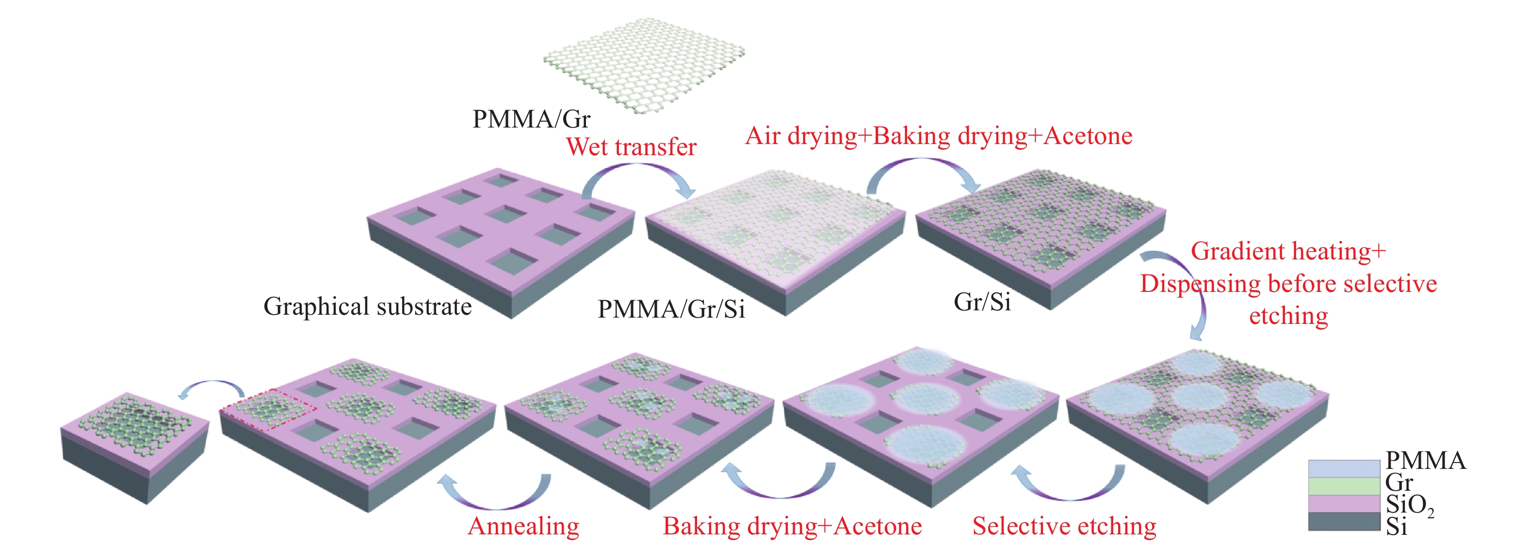
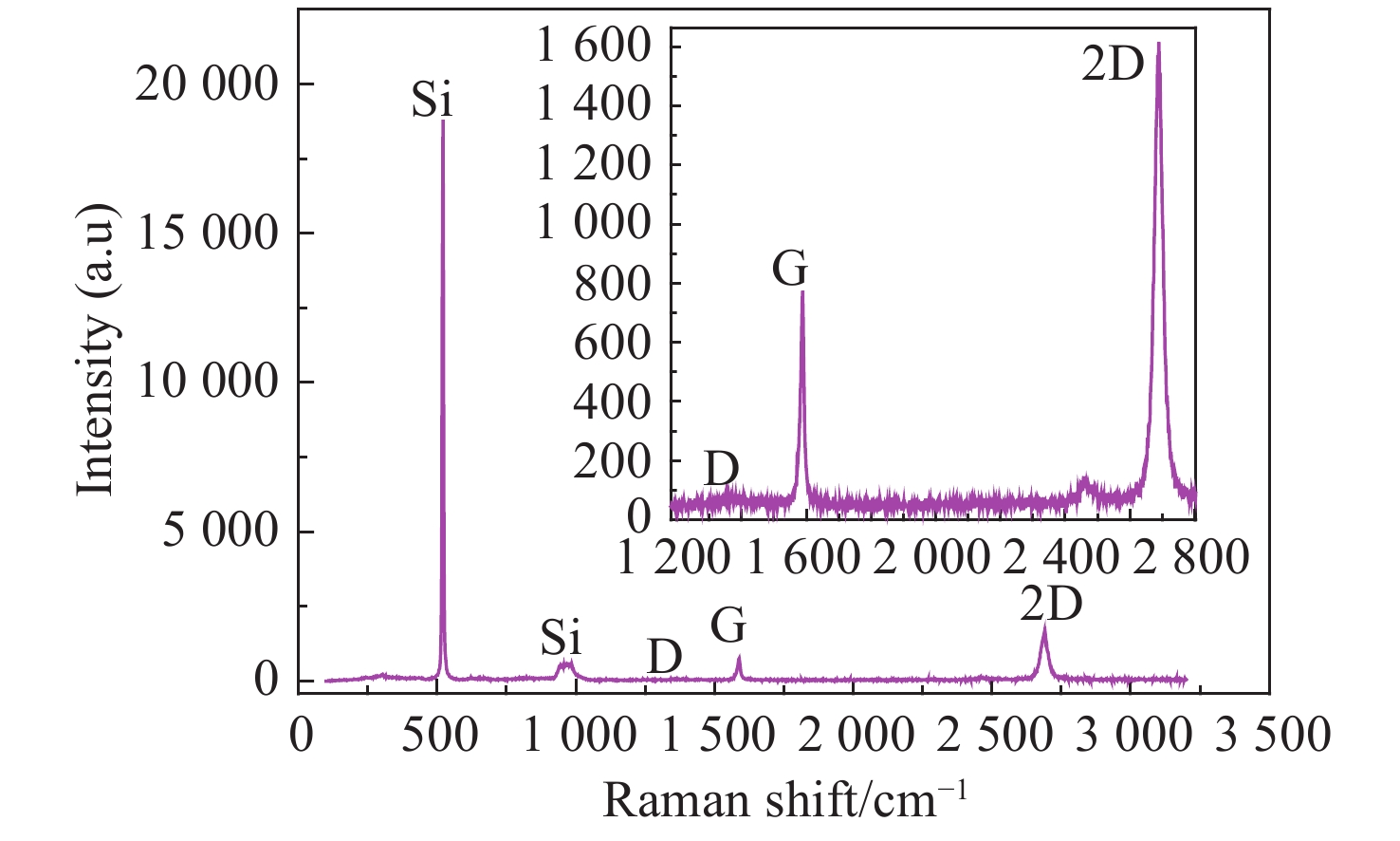
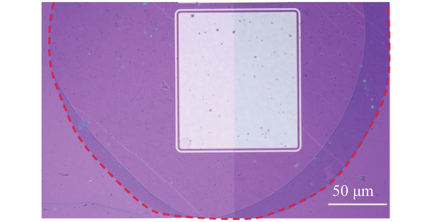
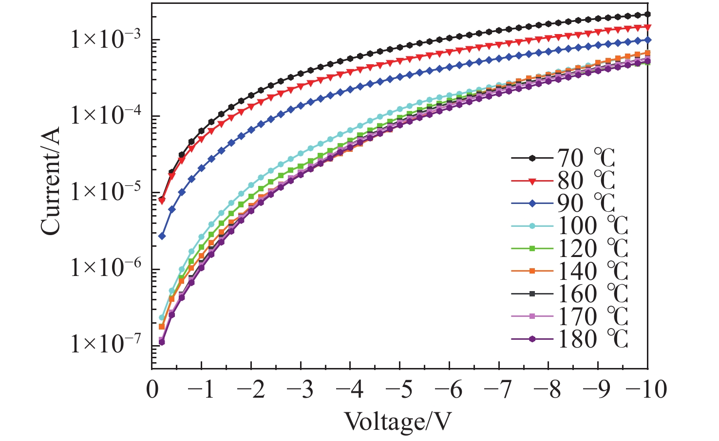
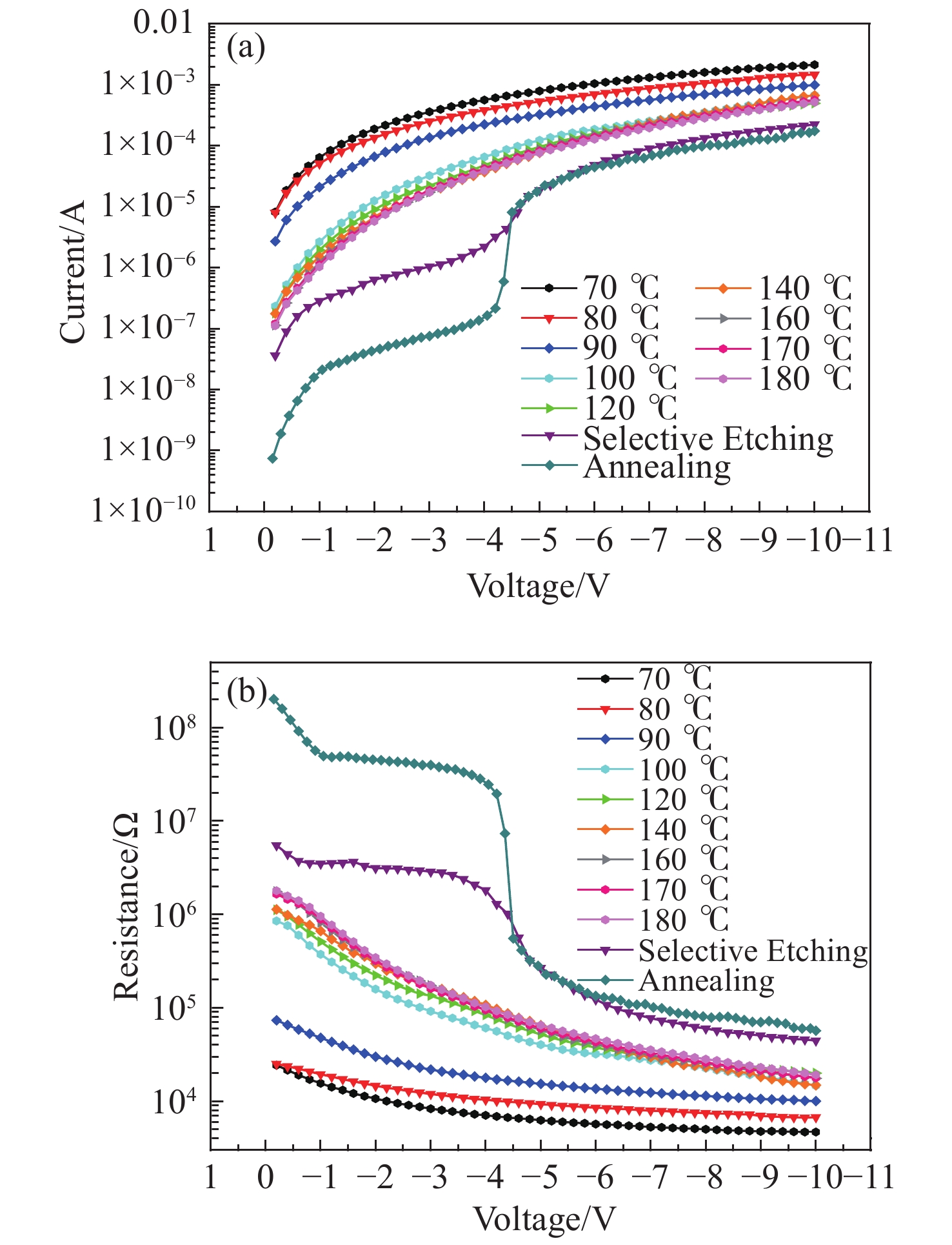
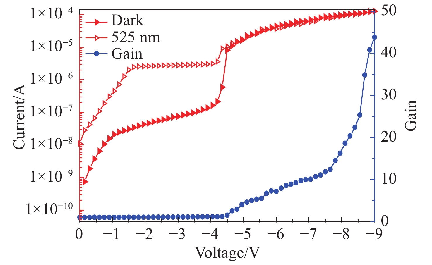
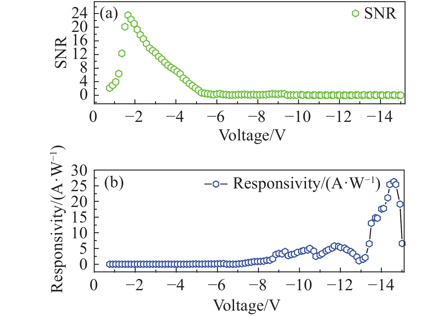
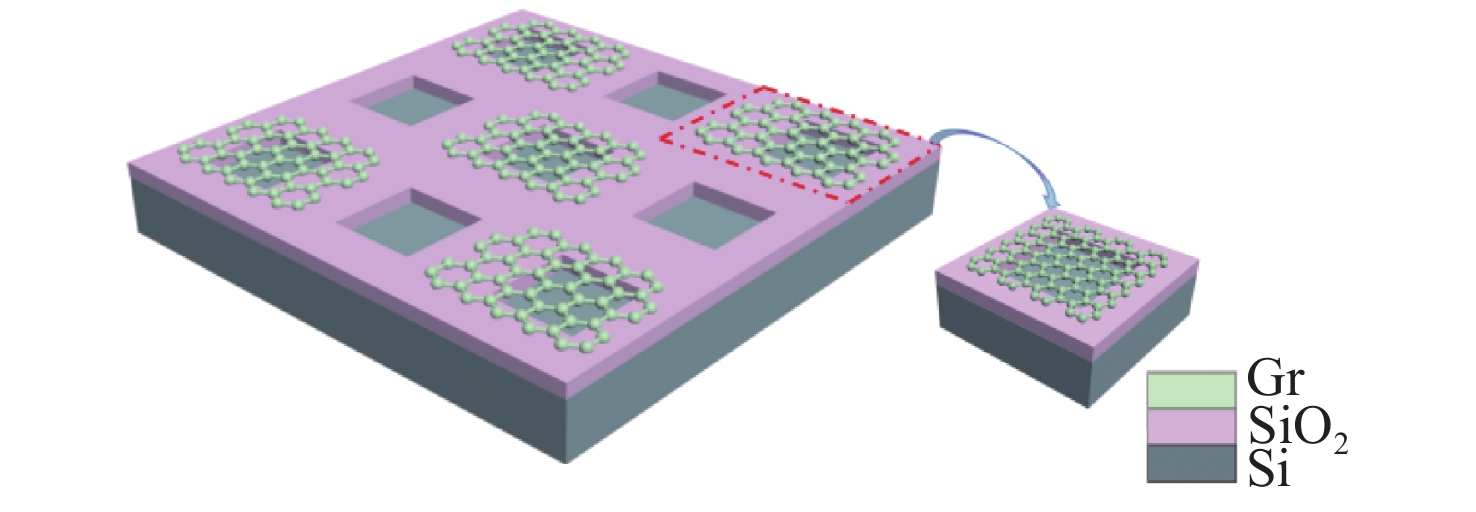
Wet transferring two-dimension (2D) material to a semiconductor substrate is a common method to prepare a hetero-junction photodetector. When preparing to wet transfer a hetero-junction, different preparation details have significant effects on the properties of the hetero-junction formed by the 2D materials and semiconductors. In this paper, a series of identical Gr/Si hetero-junction devices were prepared by the wet transfer method and the relationship between its preparation technique and the voltage-current characteristics was studied in detail. The experimental results show that the gradient drying process can significantly reduce the dark current of the Gr/Si hetero-junction photodetector, the optimal drying temperature peak is 170 °C, and the leakage current basically no longer changes above 170 °C. The surface impurities and residual water in the inter-layer of Gr/Si van der Waals hetero-junction has a significant effect on the leakage current of the hetero-junction. The selective etching and annealing process of a Gr/Si van der Waals hetero-junction can also greatly reduce the leakage current. Therefore, a suitable drying process, selective etching process and annealing process are each necessary in the preparation of a Gr/Si hetero-junction photodetector. These results can give reference to the fabrication of two-dimensional material hetero-junction devices by the wet transfer method.

| [1] |
朱淼. 石墨烯/硅异质结光电探测器性能研究[D]. 北京: 清华大学, 2015.
ZHU M. Study on the graphene/silicon heterojucntion photodetectors[D]. Beijing: Tsinghua University, 2015. (in Chinese)
|
| [2] |
张翼鹏, 王雪, 纪佩璇, 等. 不同响应机制下的石墨烯基光电探测器研究进展[J]. 发光学报,2022,43(4):552-575. doi: 10.37188/CJL.20210359
ZHANG Y P, WANG X, JI P X, et al. Research progress of graphene based photodetectors under different response mechanisms[J]. Chinese Journal of Luminescence, 2022, 43(4): 552-575. (in Chinese) doi: 10.37188/CJL.20210359
|
| [3] |
公爽, 田金荣, 李克轩, 等. 新型二维材料在固体激光器中的应用研究进展[J]. 中国光学,2018,11(1):18-30. doi: 10.3788/co.20181101.0018
GONG SH, TIAN J R, LI K X, et al. Advances in new two-dimensional materials and its application in solid-state lasers[J]. Chinese Opticas, 2018, 11(1): 18-30. (in Chinese) doi: 10.3788/co.20181101.0018
|
| [4] |
胡思奇, 田睿娟, 甘雪涛. 面向硅基光电子混合集成的二维材料探测器[J]. 中国光学,2021,14(5):1039-1055. doi: 10.37188/CO.2021-0003
HU S Q, TIAN R J, GAN X T. Two-dimensional material photodetector for hybrid silicon photonics[J]. Chinese Optics, 2021, 14(5): 1039-1055. (in Chinese) doi: 10.37188/CO.2021-0003
|
| [5] |
YIN J, LIU L, ZANG Y SH, et al. Engineered tunneling layer with enhanced impact ionization for detection improvement in graphene/silicon heterojunction photodetectors[J]. Light:Science &Applications, 2021, 10(1): 113.
|
| [6] |
LI X M, ZHU M, DU M D, et al. High detectivity graphene-silicon heterojunction photodetector[J]. Small, 2016, 12(5): 595-601. doi: 10.1002/smll.201502336
|
| [7] |
王学军. 基于二维纳米材料生物传感及光电探测技术的研究[D]. 上海: 华东理工大学, 2018.
WANG X J. Two-dimensional nanomaterials for biosensing and photosensing[D]. Shanghai: East China University of Science and Technology, 2018. (in Chinese)
|
| [8] |
LI F, ZHENG J B, YAO Q, et al. Recent progress of silicon integrated light emitters and photodetectors for optical communication based on two-dimensional materials[J]. Optical Materials Express, 2021, 11(10): 3298-3320. doi: 10.1364/OME.435902
|
| [9] |
GUPTA S, KUMAR R. Review—photodetection properties of graphene/silicon van der Waals heterojunction[J]. ECS Journal of Solid State Science and Technology, 2022, 11(6): 061010. doi: 10.1149/2162-8777/ac7614
|
| [10] |
韩天亮, 唐利斌, 左文彬, 等. 石墨烯异质结及其光电器件的研究进展[J]. 红外技术,2021,43(12):1141-1157.
HAN T L, TANG L B, ZUO W B, et al. Research progress of graphene heterojunctions and their optoelectronic devices[J]. Infrared Technology, 2021, 43(12): 1141-1157. (in Chinese)
|
| [11] |
DAVYDOVSKAYA D. Photoconductivity in high-quality graphene[D]. Barcelona: Universitat Politècnica de Catalunya, 2015.
|
| [12] |
张金月, 吕俊鹏, 倪振华. 二维材料异质结高灵敏度红外探测器[J]. 中国光学,2021,14(1):87-99. doi: 10.37188/CO.2020-0139
ZHANG J Y, LYU J P, NI ZH H. Highly sensitive infrared detector based on a two-dimensional heterojunction[J]. Chinese Optics, 2021, 14(1): 87-99. (in Chinese) doi: 10.37188/CO.2020-0139
|
| [13] |
AESCHLIMANN S, ROSSI A, CHÁVEZ-CERVANTES M, et al. Direct evidence for efficient ultrafast charge separation in epitaxial WS2/graphene heterostructures[J]. Science Advances, 2020, 6(20): eaay0761. doi: 10.1126/sciadv.aay0761
|
| [14] |
ULLAH S, YANG X Q, TA H Q, et al. Graphene transfer methods: a review[J]. Nano Research, 2021, 14(11): 3756-3772. doi: 10.1007/s12274-021-3345-8
|
| [15] |
杨珏晗, 魏钟鸣, 牛智川. 基于二维材料异质结的光探测器研究进展[J]. 人工晶体学报,2020,49(3):379-397. doi: 10.3969/j.issn.1000-985X.2020.03.001
YANG J H, WEI ZH M, NIU ZH CH. Recent progress on two-dimensional heterostructure based photodetectors[J]. Journal of Synthetic Crystals, 2020, 49(3): 379-397. (in Chinese) doi: 10.3969/j.issn.1000-985X.2020.03.001
|
| [16] |
廖俊懿, 吴娟霞, 党春鹤, 等. 二维材料的转移方法[J]. 物理学报,2021,70(2):028201. doi: 10.7498/aps.70.20201425
LIAO J Y, WU J X, DANG CH H, et al. Methods of transferring two-dimensional materials[J]. Acta Physica Sinica, 2021, 70(2): 028201. (in Chinese) doi: 10.7498/aps.70.20201425
|
| [17] |
吴玉玲, 毕瑞可, 张杰, 等. 石墨烯湿法转移过程工艺优化[J]. 微纳电子技术,2017,54(8):565-569,579.
WU Y L, BI R K, ZHANG J, et al. Optimization of the wet transfer technique of graphene[J]. Micronanoelectronic Technology, 2017, 54(8): 565-569,579. (in Chinese)
|
| [18] |
李春, 胡晓影, 何天应, 等. 二维原子晶体半导体转移技术研究进展[J]. 深圳大学学报理工版,2018,35(3):257-266. doi: 10.3724/SP.J.1249.2018.03257
LI CH, HU X Y, HE T Y, et al. Recent progress on transfer techniques of two-dimensional atomically thin semiconductor[J]. Journal of Shenzhen University Science and Engineering, 2018, 35(3): 257-266. (in Chinese) doi: 10.3724/SP.J.1249.2018.03257
|
| [19] |
徐杨, 万霞, 郭宏伟, 等. 基于石墨烯/二氧化硅/硅的雪崩光电探测器及制备方法: 中国, CN104300027A[P]. 2015-01-21.
XU Y, WAN X, GUO H W, et al. . Avalanche photodetector and preparation method based on graphene/silica/silicon: CN, 104300027A[P]. 2015-01-21. (in Chinese)
|
| [20] |
王雪. 基于石墨烯/硅肖特基结的光电探测器的研制[D]. 杭州: 浙江大学, 2016.
WANG X. Photodetectors based on graphene/silicon schottky diode[D]. Hangzhou: Zhejiang University, 2016. (in Chinese)
|
| [21] |
WANG Y M, YANG SH M, LAMBADA D R, et al. A graphene-silicon Schottky photodetector with graphene oxide interlayer[J]. Sensors and Actuators A:Physical, 2020, 314: 112232. doi: 10.1016/j.sna.2020.112232
|
| [22] |
LIANG X L, SPERLING B A, CALIZO I, et al. Toward clean and crackless transfer of graphene[J]. ACS Nano, 2011, 5(11): 9144-9153. doi: 10.1021/nn203377t
|
| [23] |
HAN J Y, WANG J. Photodetectors based on two-dimensional materials and organic thin-film heterojunctions[J]. Chinese Physics B, 2019, 28(1): 017103. doi: 10.1088/1674-1056/28/1/017103
|
| [24] |
李云杰, 付津滔, 聂长斌, 等. 石墨烯/硅异质结光电导型探测器光电响应及噪声[J]. 微纳电子技术,2022,59(8):732-741. doi: 10.13250/j.cnki.wndz.2022.08.002
LI Y J, FU J T, NIE CH B, et al. Photoresponse and noise of graphene/silicon heterojunction photoconductive detector[J]. Micronanoelectronic Technology, 2022, 59(8): 732-741. (in Chinese) doi: 10.13250/j.cnki.wndz.2022.08.002
|
Figures(9)


 DownLoad: