


-
摘要:
为了解决光子芯片垂直端面光波导桥接过程中,由于光子芯片表面遮挡激光束而引发的光波导形状缺陷问题,基于高数值孔径物镜聚焦光场分布,研究了激光焦点在光子芯片垂直端面不同
x 方向偏移距离处的光强分布特征。首先,给出了高数值孔径物镜聚焦系统中焦点附近光场分布的解析表达式,以及线偏振光入射时的聚焦光场分量表达式。然后,通过给出的表达式进行数值模拟,研究了激光焦点在距离光子芯片垂直端面不同x 方向偏移距离处的焦点光强分布,揭示了焦点光场受到干扰时的强度变化,并绘制出焦点光场强度变化曲线。该曲线与实验中观测到的光波导形状变化趋势相符。最后,基于焦点光强分布曲线,反向推导出了激光功率补偿系数曲线。并将其应用于光波导补偿加工实验中,经过功率补偿加工后,光波导宽度小于4 μm的部分被成功补偿至4 μm,而且形态变得更加笔直,缺陷得到有效修复。数值模拟计算和实验结果表明:该方法成功弥补了由激光功率不足引起的光波导形状缺陷,为光子芯片集成耦合领域的光波导加工制备提供了有效的解决途径。Abstract:To address the issue of shape defects in optical waveguides that occur due to the laser beam being obstructed by the surface of the photonic chip during the vertical end-face waveguide bridging process in photonic chips. Based on the focusing light field of high numerical aperture (NA) objective lenses, the characteristics of light intensity distribution at various
x -direction offset distances of the laser focus from the vertical end-face of the photonic chip are investigated. First, we give the analytical expressions of the light field near the focus. These are in the focusing system of high NA lenses. Firstly, analytical expressions for the light field distribution near the focal point in the focusing system of a high numerical aperture (NA) objective lens are presented, along with expressions for the components of the focused light field when linearly polarized light is incident. Then, numerical simulations are conducted with the provided expressions, the focal light intensity distribution of the laser focus at differentx -direction offset distances from the vertical end-face of the photonic chip is studied. The intensity variations of the focal light field when subjected to disturbances are revealed, and curves depicting the intensity changes of the focal light field are plotted. These curves align with the observed trends in the shape changes of the optical waveguide during experiments. Finally, based on the focal light intensity distribution curves, the laser power compensation coefficients curves are derived in reverse. These are then applied to the optical waveguide compensation processing experiments. It can be seen that after power compensation processing, the sections of the optical waveguide with a width less than 4 μm are successfully compensated to 4 μm. Moreover, the morphology became straighter, and the defects are effectively repaired. The results of numerical calculation simulations and experiments demonstrate that this method successfully compensates for the shape defects of optical waveguides caused by insufficient laser power, providing an effective solution for the fabrication and processing of optical waveguides in the field of photonic chip integrated coupling. -
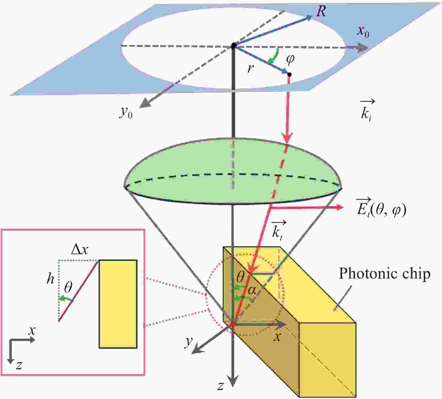
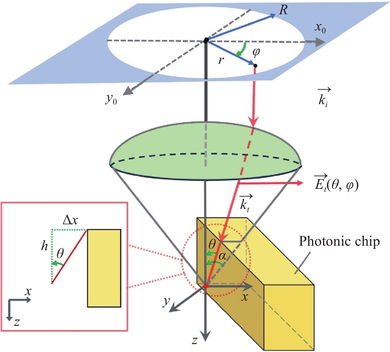
图 1 光子芯片垂直端面处聚焦场分布的几何图形和所涉及变量的示意图
Figure 1. Schematic diagram of the geometric pattern of the focal field distribution at the vertical end-face of a photonic chip and the variables involved
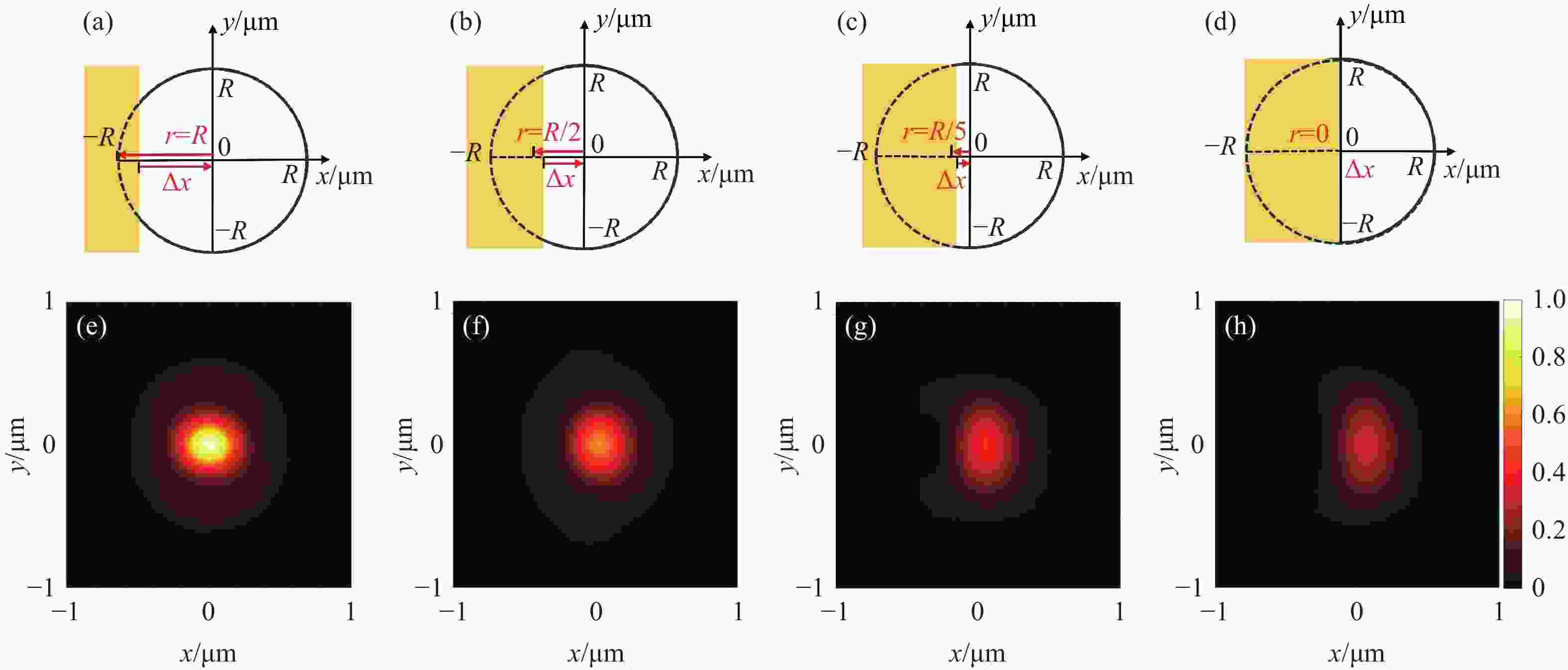
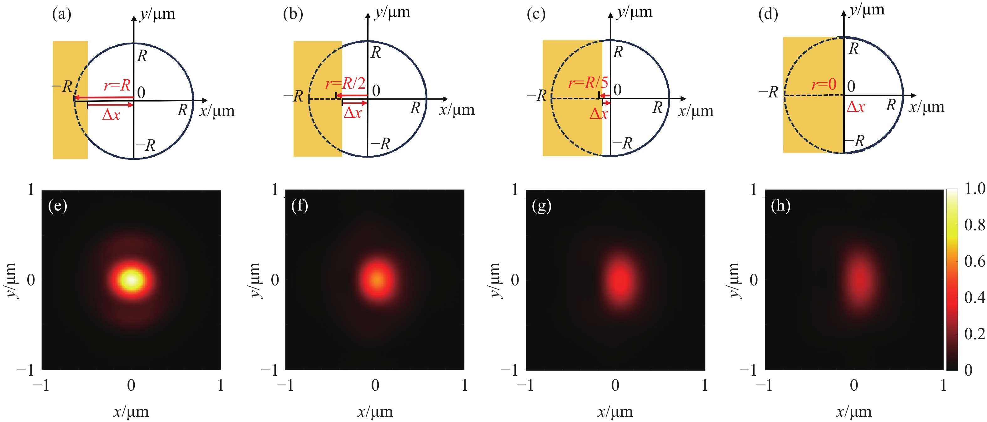
图 2 聚焦光束受遮挡区域 (a)~(d) 及其对应的焦点处 xy 截面的光场强度分布(e)~(h)。其中,光子芯片垂直面与焦点之间的x方向上偏移距离:(a),(e) ∆x =3.8 μm;(b),(f) ∆x =1.6 μm;(c),(g) ∆x =0.6 μm;(d),(h) ∆x =0 μm
Figure 2. Occluded region of the focused beam (a)-(d) and the corresponding light field intensity distribution in the xy section at the focal point (e)-(h). The offset distances in the x direction between the vertical plane of the photon chip and the focus are as follows: (a), (e) ∆x = 3.8 μm; (b), (f) ∆x = 1.6 μm; (c), (g) ∆x = 0.6 μm; and (d), (h) ∆x = 0 μm
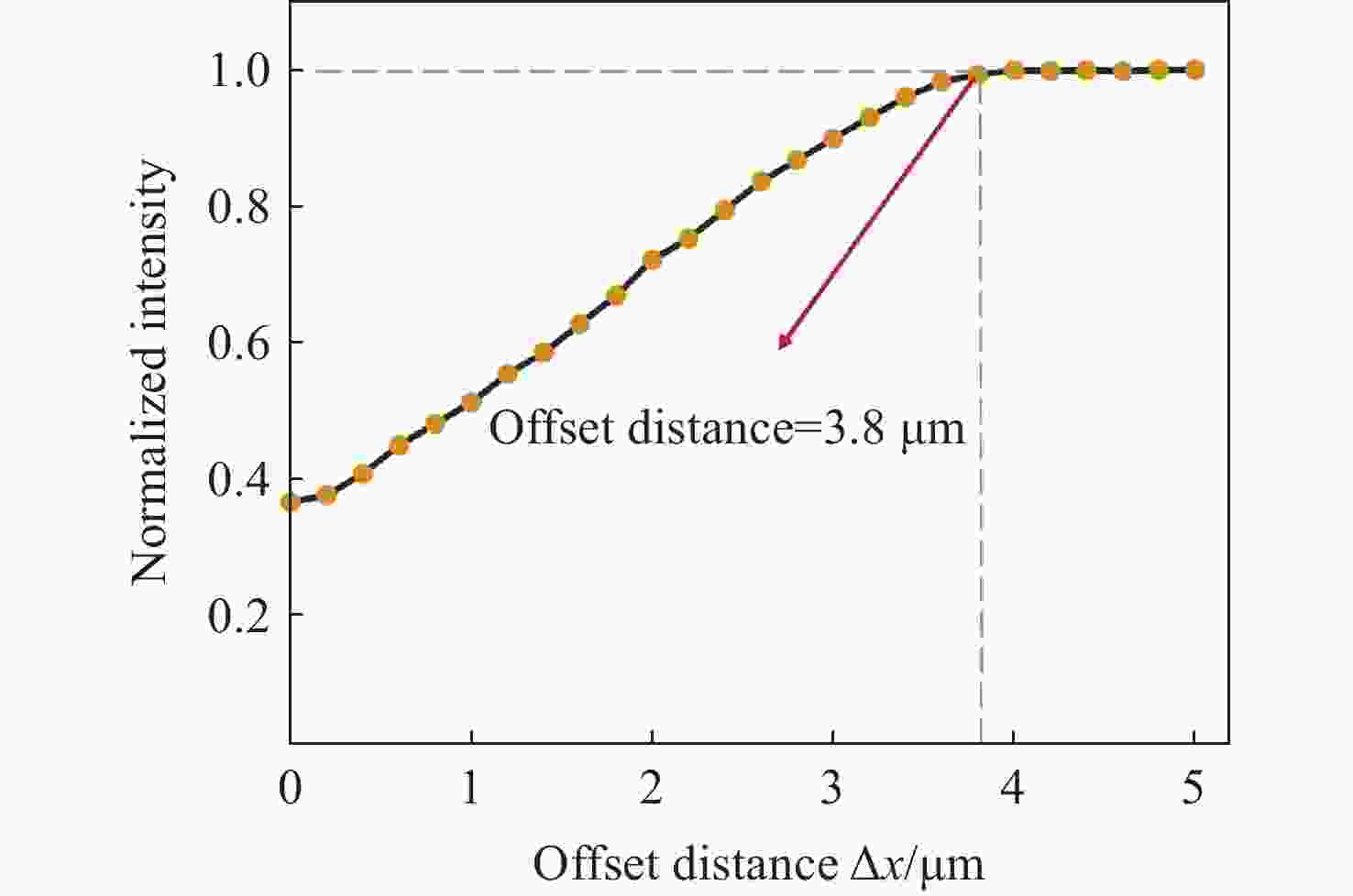
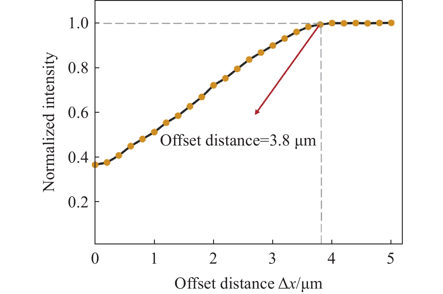
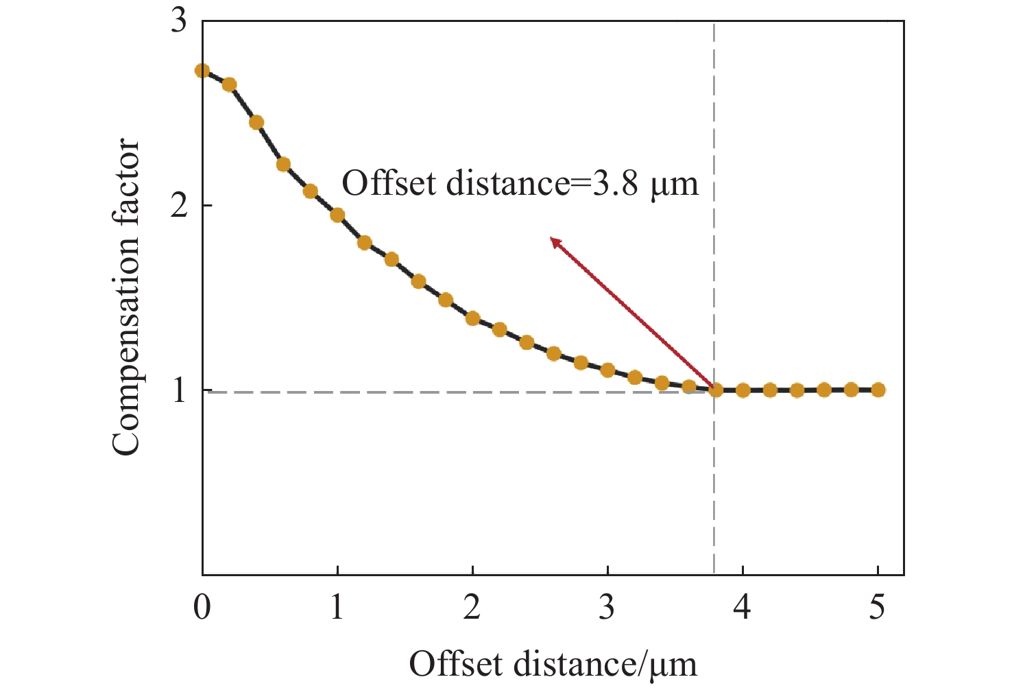
图 3 焦点光强分布的归一化最大值与光子桥接系统焦点和光子芯片垂直面之间x方向上偏移距离的关系曲线图
Figure 3. Relationship between normalized maximum of focal intensity distribution and offset distance in the x direction between the focal point of the photonic bridge system and the vertical plane of the photonic chip
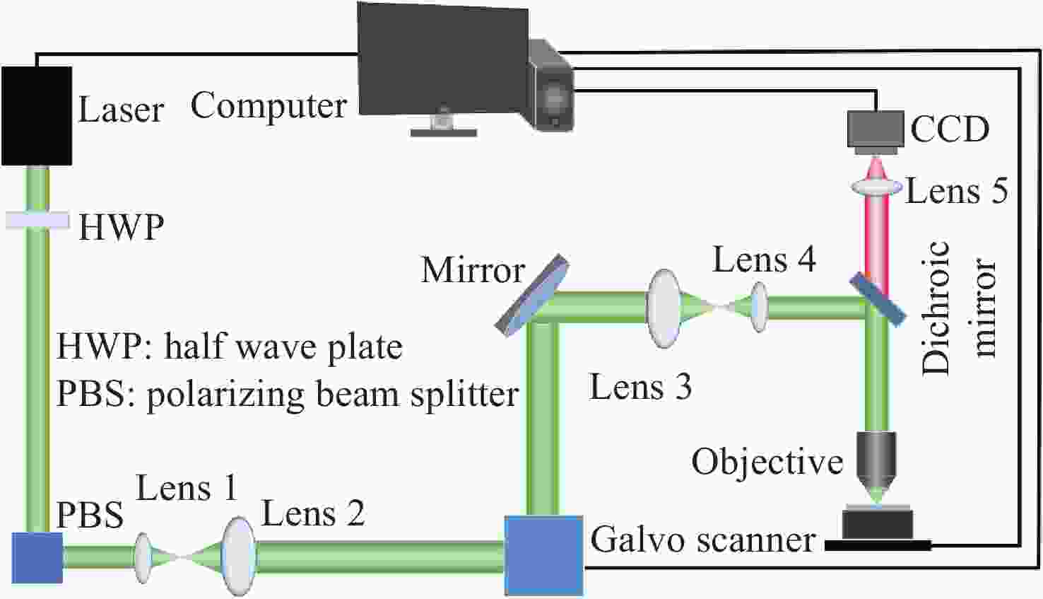
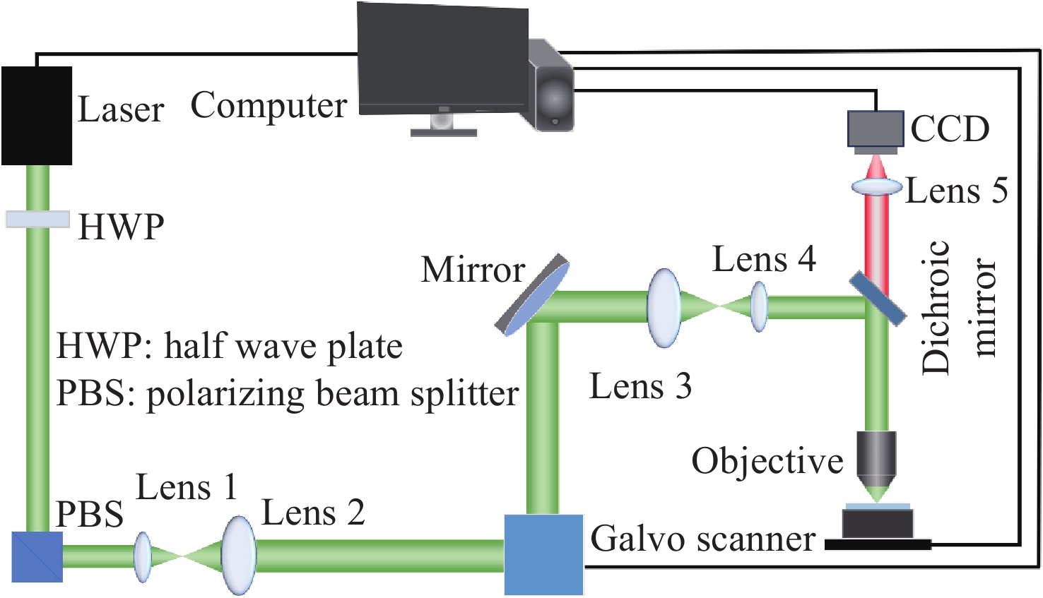
图 4 飞秒激光直写系统光路图
Figure 4. Optical path diagram of femtosecond laser direct writing system
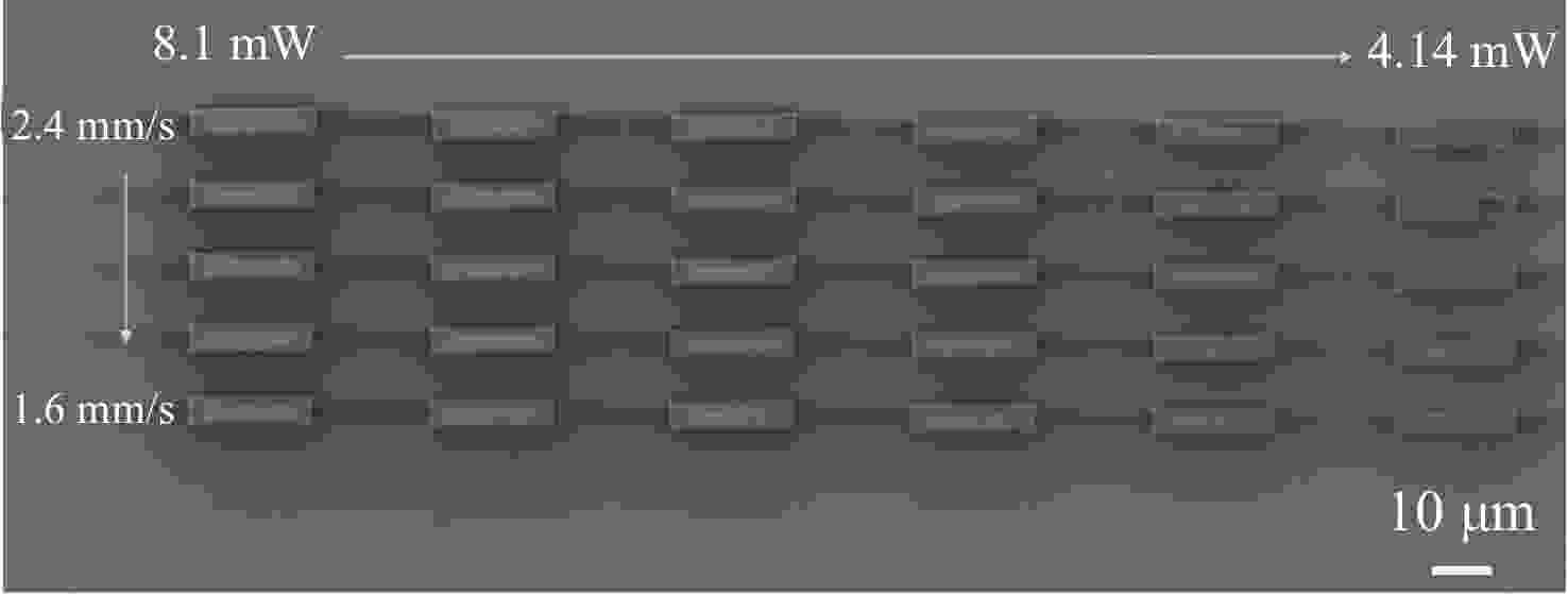
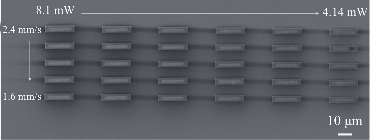
图 5 加工速度和功率渐变的光波导结构阵列电镜图
Figure 5. Electron microscopy of an optical waveguide structure array with varying processing speeds and power gradients
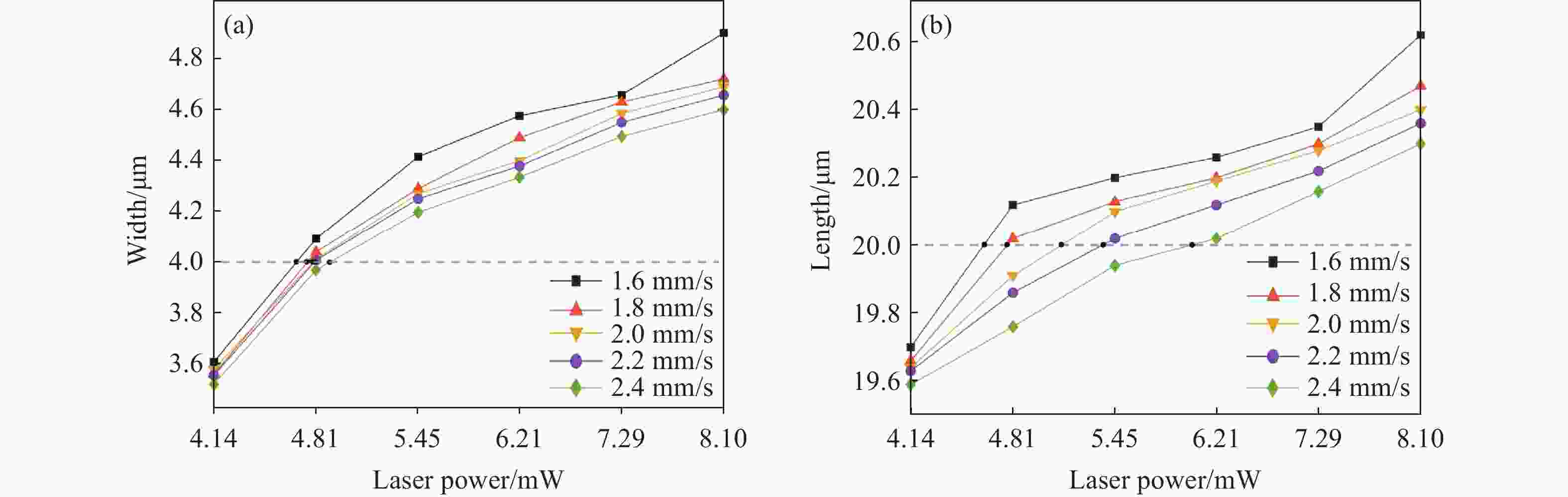
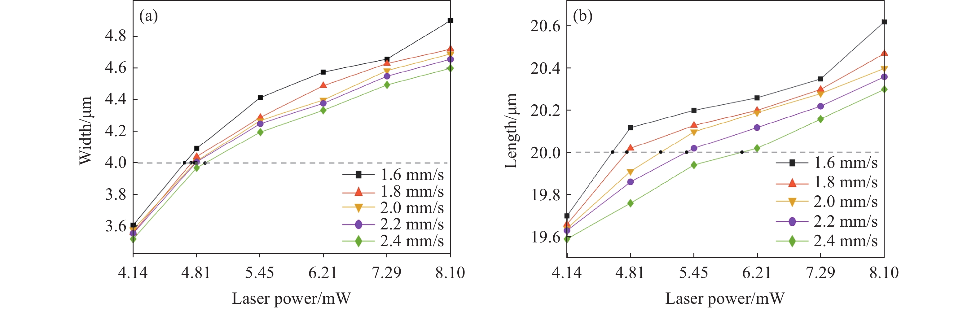
图 6 光波导的(a)宽度和(b)长度与光子桥接加工速度和功率的关系曲线图
Figure 6. Plot of (a) width and (b) length of optical waveguide varying with processing speed and power for photonic bridging
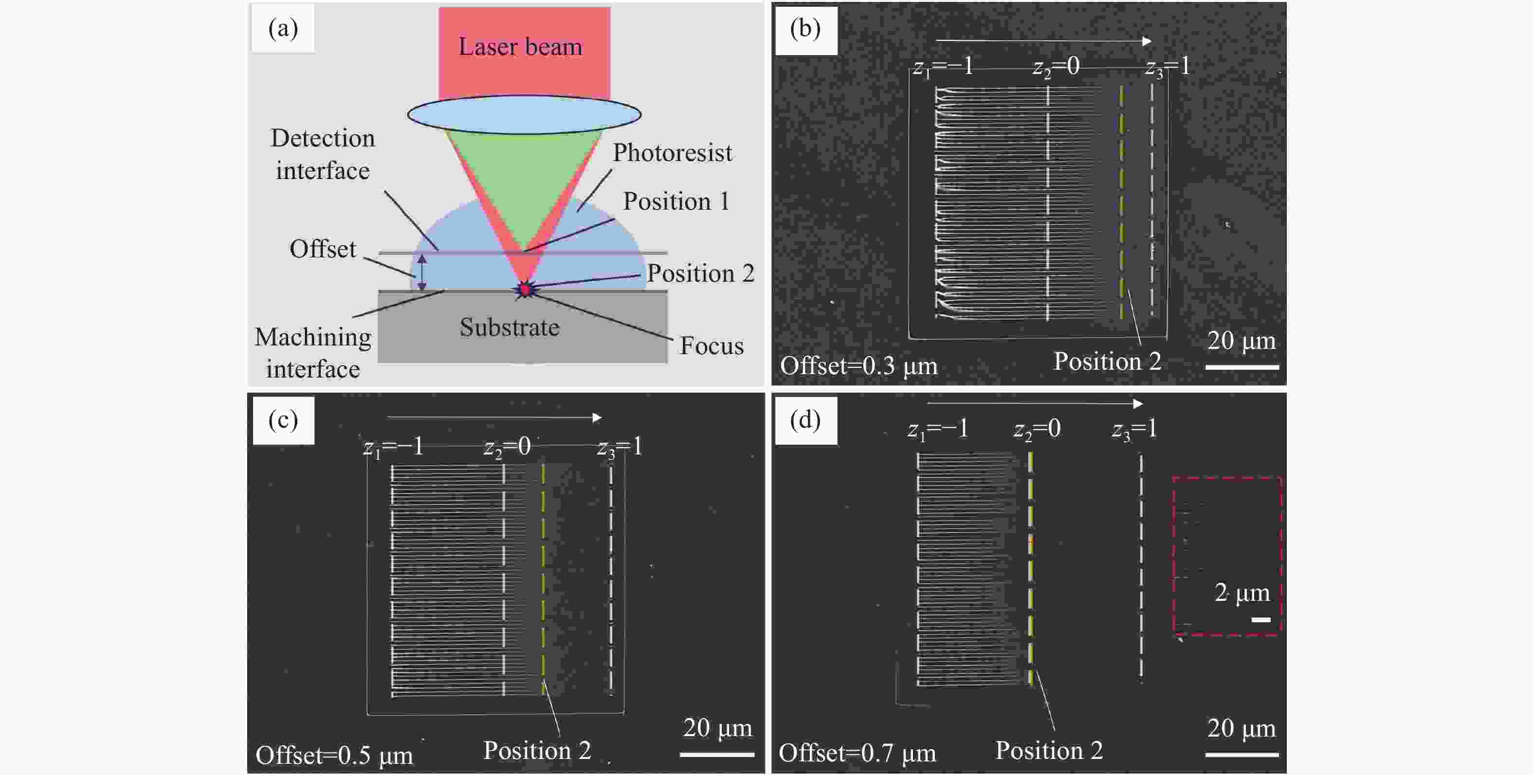
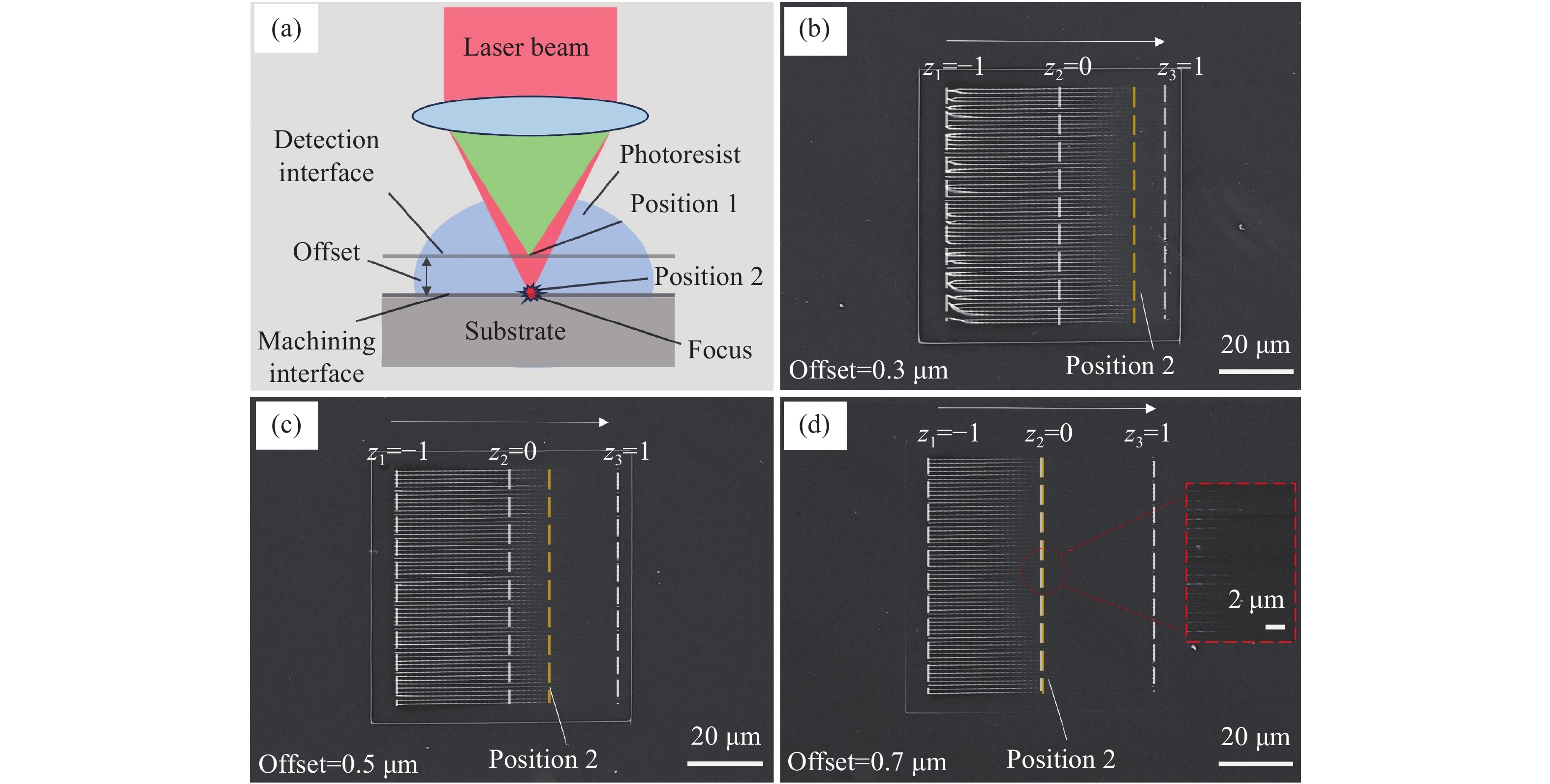
图 7 (a) 探测位置和实际加工位置在z方向上存在偏差值的示意图。(b)~(d) 偏差值分别为0.3 μm,0.5 μm和0.7 μm时的加工结果
Figure 7. (a) Schematic diagram of the deviation value in the z direction between the detection position of the detection light and the actual processing position. (b)-(d) Processing results when the offset is (b) 0.3 μm, (c) 0.5 μm, (d) 0.7 μm
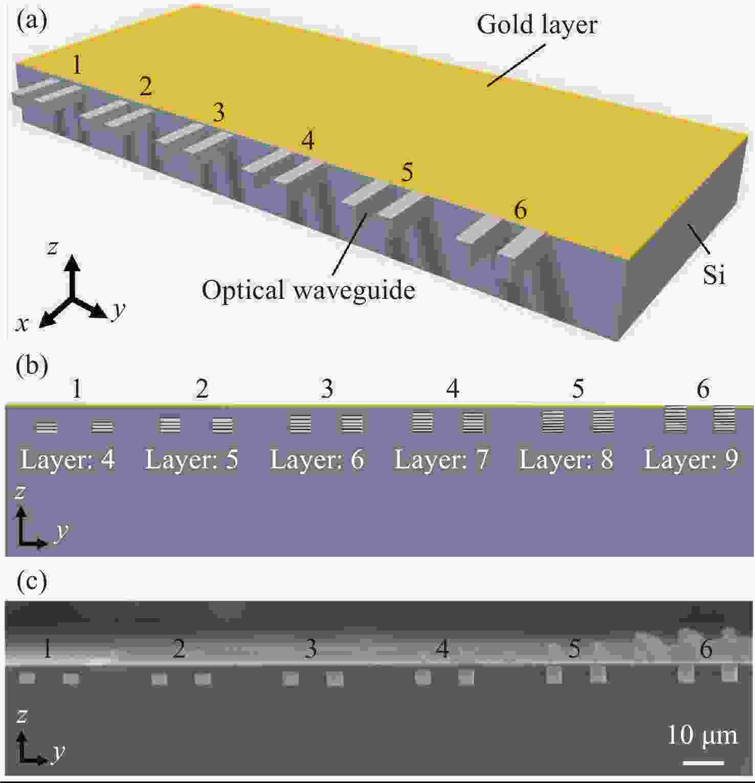
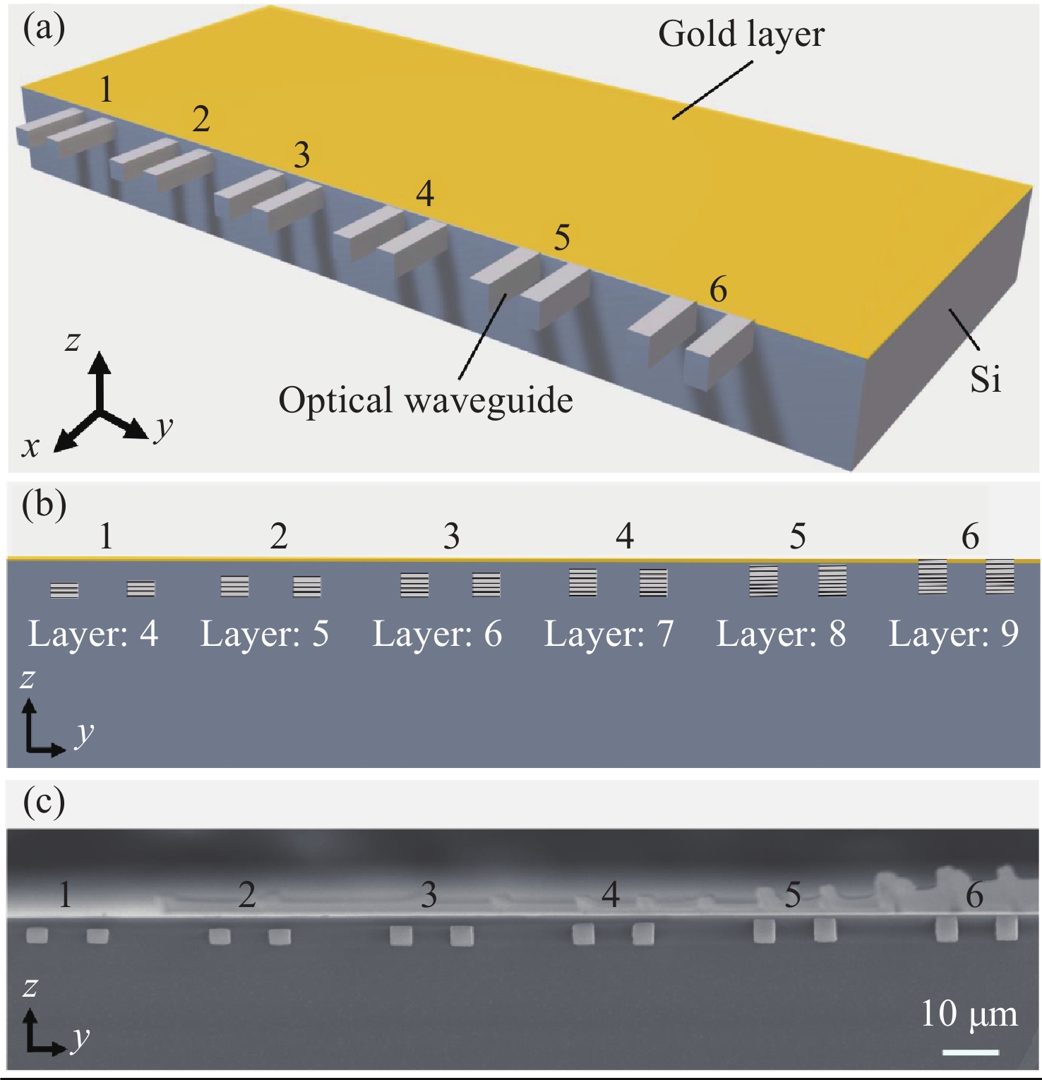
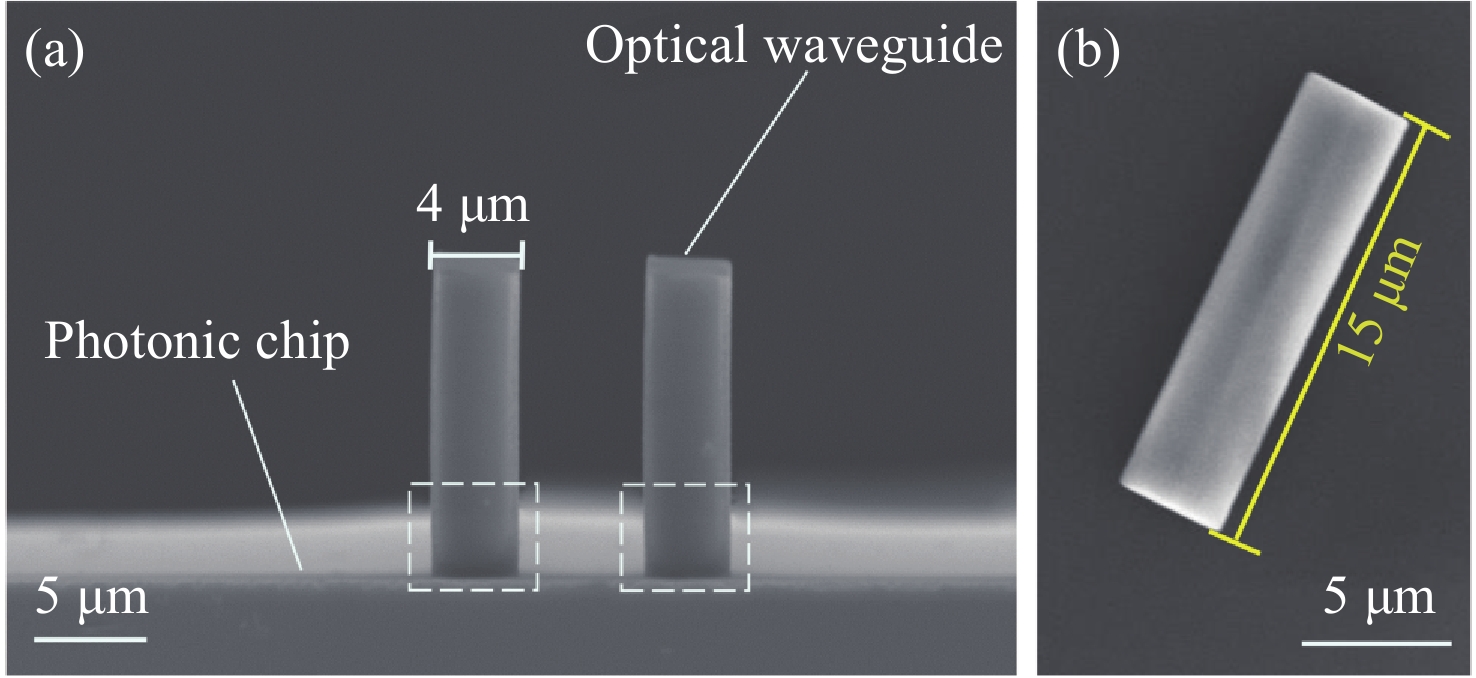
图 8 (a)光子芯片垂直面上加工光波导阵列的三维示意图;(b)三维模型的yz面示意图;(c)光子芯片垂直端面上实际加工出的6组光波导的电镜图
Figure 8. (a) Three-dimensional diagram of optical waveguide array machined on vertical face of photonic chip; (b) yz plane diagram of the 3D model; (c) electron microscope images of 6 groups of optical waveguides actually machined on vertical end face of photonic chip
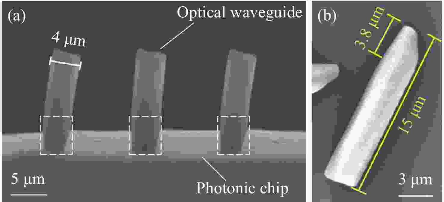
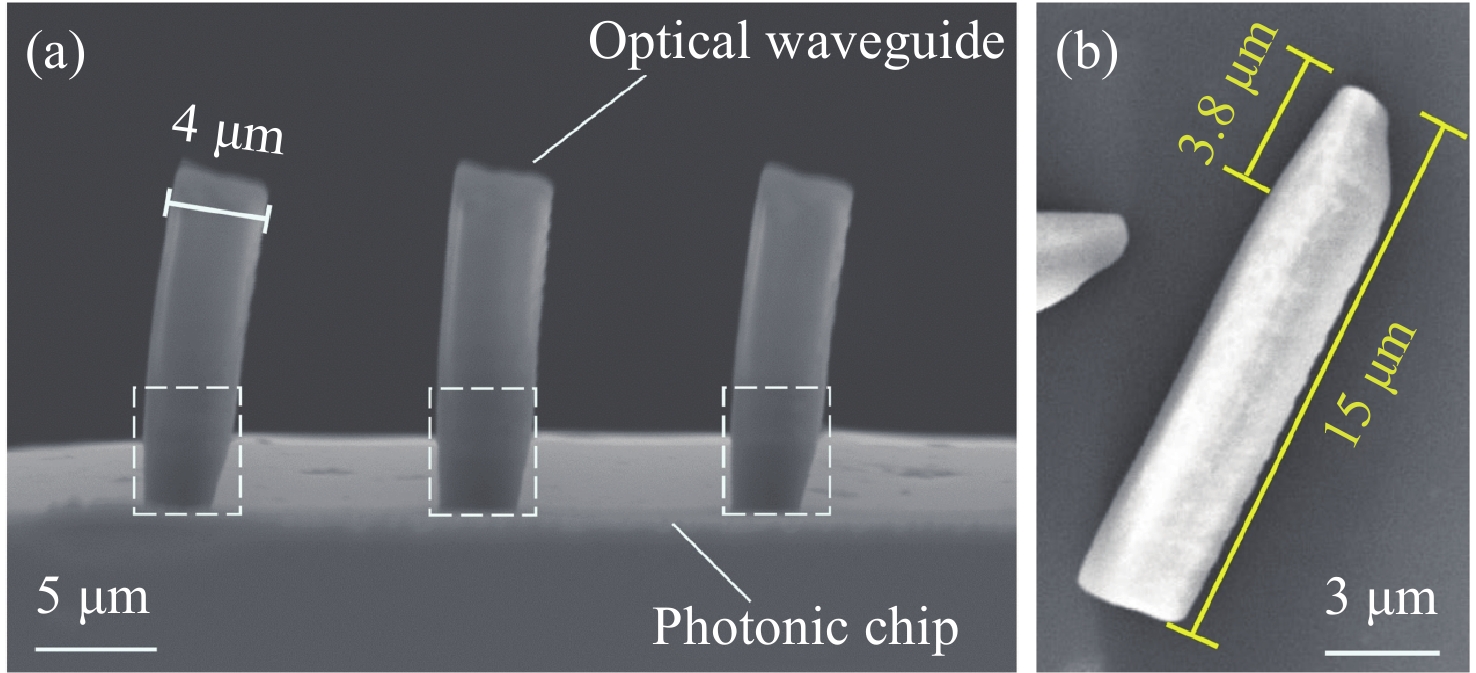
图 9 在光子芯片垂直面上加工的未经功率补偿的光波导(a)站立和(b)倒置电镜图
Figure 9. (a) Standing and (b) inverted electron microscopy images of uncompensated optical waveguide machined on vertical surface of photonic chip
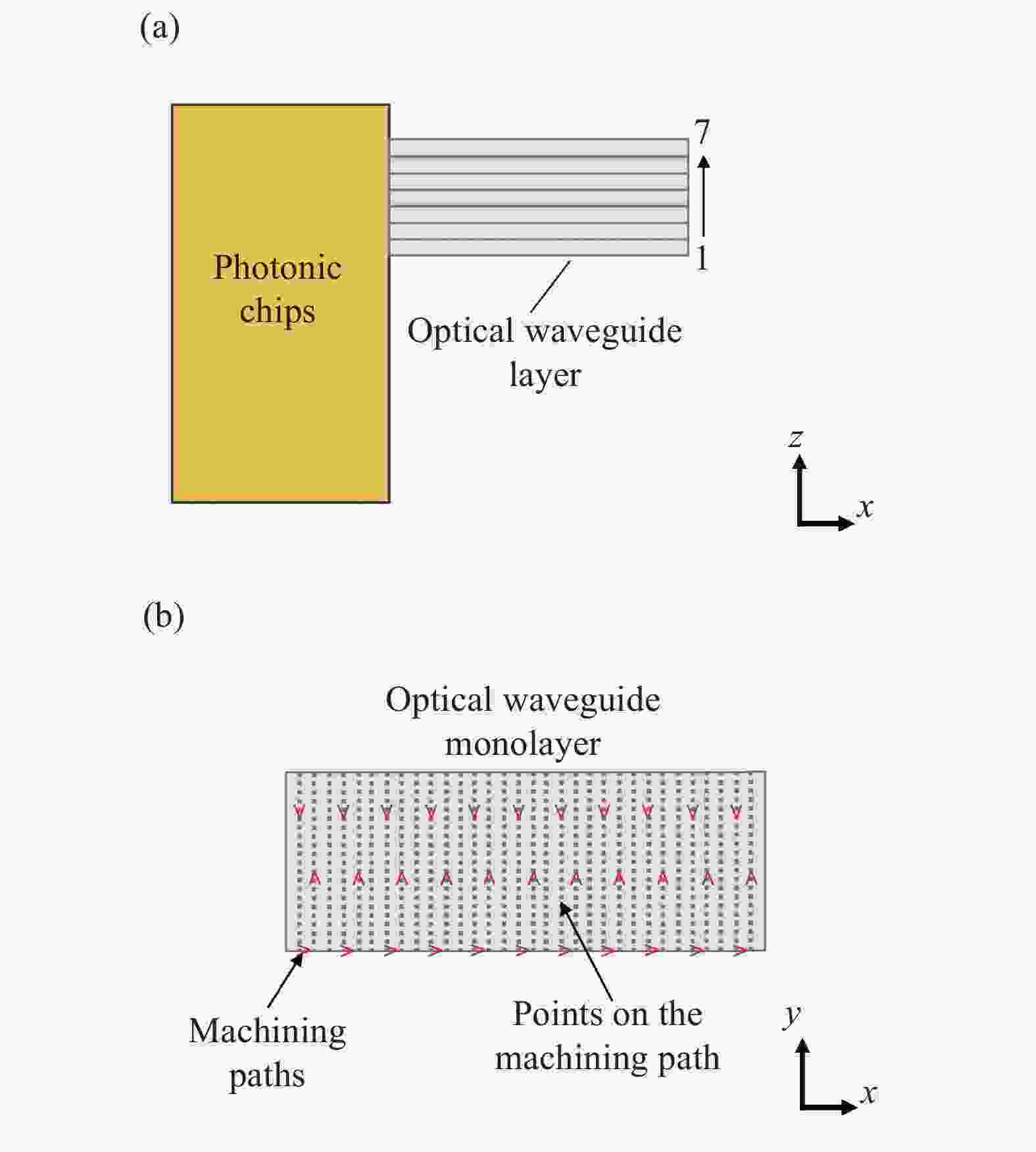
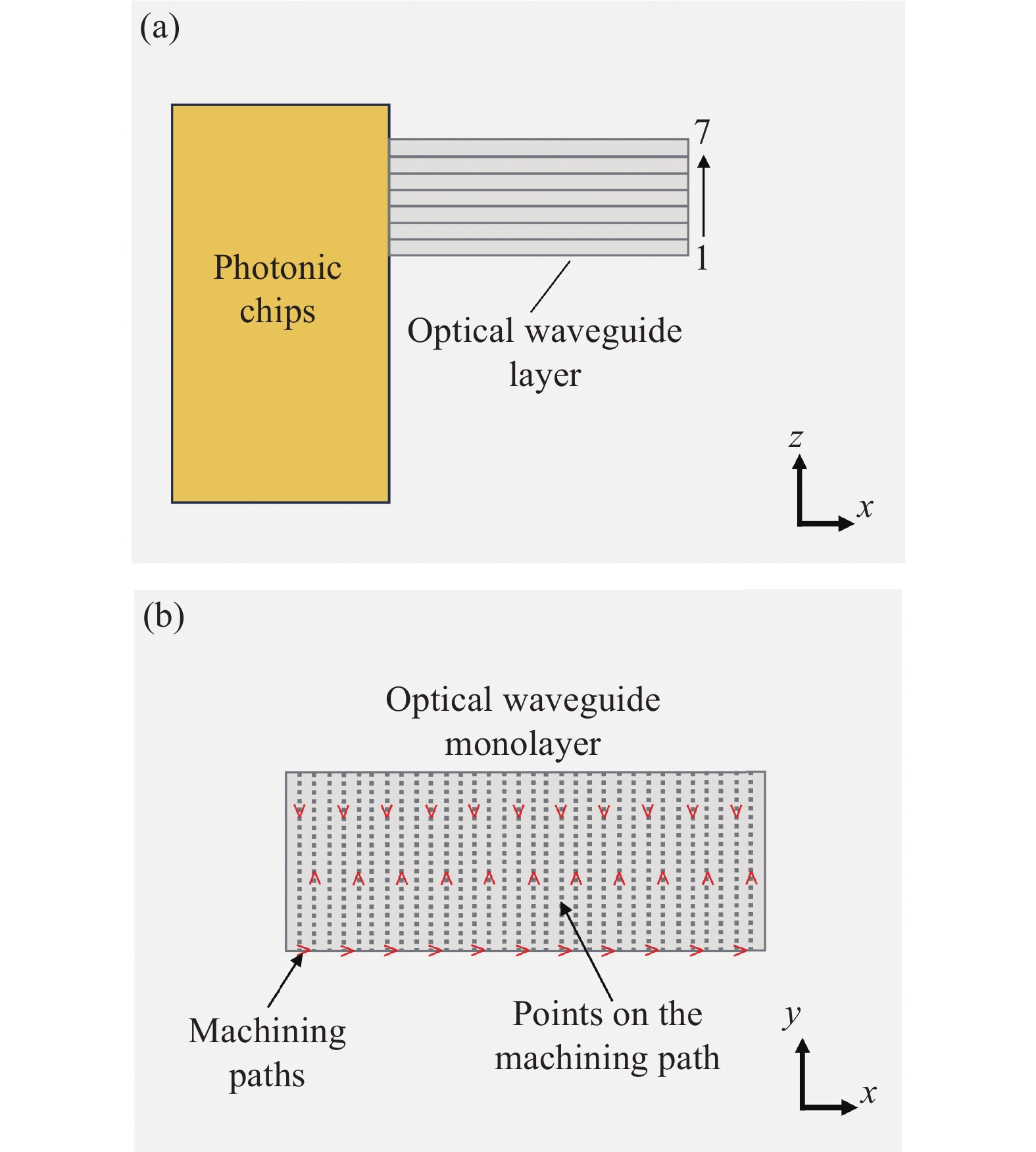
图 11 (a)光子芯片垂直端面上加工光波导结构时,将光波导沿z轴分层的示意图;(b)光波导分出的单层,箭头代表加工路径,黑色点代表加工路径上的每个位置点
Figure 11. (a) optical waveguide structure processed on vertical end face of the photonic chip, showing the schematic layer along the z-axis.; (b) single layer separated by the optical waveguide, with the arrow representing the machining path and the black dots representing each position point on the machining path
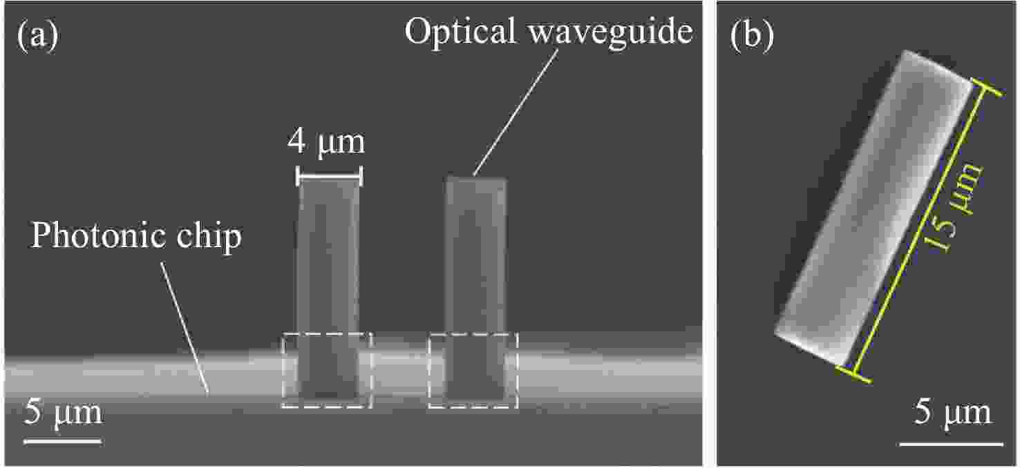
图 12 在光子芯片垂直面上加工的功率补偿后站立和倒置的光波导电镜图。(a)垂直端面上加工的功率补偿后的光波导;(b)功率补偿后的光波导倒置形态
Figure 12. Standing and inverted optical waveguide electron microscopy images after power compensation machining on the vertical surface of a photonic chip. (a) Power compensated optical waveguide machined on vertical end face; (b) inverted optical waveguide configuration after power compensation
表 1 光波导高度随加工层数的变化
Table 1. Variation of optical waveguide height with the number of processing layers
波导序号 1 2 3 4 5 6 加工层数 4 5 6 7 8 9 波导高(μm) 2.51 2.98 3.53 4.02 4.63 5.20  下载: 导出CSV
-
[1] 冯萧萧, 韩明宇, 陈美鹏, 等. 运动探测及可见光通信一体化氮化物光电子芯片[J]. 中国光学(中英文),2023,16(5):1257-1272. doi: 10.37188/CO.2023-0028FENG X X, HAN M Y, CHEN M P, et al. Integrated Nitride optoelectronic chip for motion detection and visible light communication[J]. Chinese Optics, 2023, 16(5): 1257-1272. (in Chinese). doi: 10.37188/CO.2023-0028 [2] JIMENEZ GORDILLO O A, NOVICK A, WANG O L, et al. Fiber-chip link via mode division multiplexing[J]. IEEE Photonics Technology Letters, 2023, 35(19): 1071-1074. doi: 10.1109/LPT.2023.3298771 [3] LUO W, CAO L, SHI Y ZH, et al. Recent progress in quantum photonic chips for quantum communication and internet[J]. Light: Science & Applications, 2023, 12(1): 175. [4] LI S M, CUI ZH Z, YE X W, et al. Chip-based microwave-photonic radar for high-resolution imaging[J]. Laser & Photonics Reviews, 2020, 14(10): 1900239. [5] NEVLACSIL S, MUELLNER P, MAESE-NOVO A, et al. Multi-channel swept source optical coherence tomography concept based on photonic integrated circuits[J]. Optics Express, 2020, 28(22): 32468-32482. doi: 10.1364/OE.404588 [6] SUN B SH, MOSER S, JESACHER A, et al. Fast, precise, high contrast laser writing for photonic chips with phase aberrations[J]. Laser & Photonics Reviews, 2024, 18(9): 2300702. [7] WANG J, CAI CH K, CUI F, et al. Tailoring light on three-dimensional photonic chips: a platform for versatile OAM mode optical interconnects[J]. Advanced Photonics, 2023, 5(3): 036004. [8] MA Y X, ZHAO J, YANG T T, et al. Hybrid-integrated 200 Gb/s REC-DML array transmitter based on photonic wire bonding technology[J]. Chinese Optics Letters, 2024, 22(8): 081401. doi: 10.3788/COL202422.081401 [9] HAN X Y, CHAO M, SU X X, et al. Multiband signal receiver by using an optical bandpass filter integrated with a photodetector on a chip[J]. Micromachines, 2023, 14(2): 331. doi: 10.3390/mi14020331 [10] ZHANG W F, WANG B. On-chip reconfigurable microwave photonic processor[J]. Chinese Journal of Electronics, 2023, 32(2): 334-342. doi: 10.23919/cje.2020.00.273 [11] 杜悦宁, 陈超, 秦莉, 等. 硅光子芯片外腔窄线宽半导体激光器[J]. 中国光学,2019,12(2):229-241. doi: 10.3788/co.20191202.0229DU Y N, CHEN CH, QIN L, et al. Narrow linewidth external cavity semiconductor laser based on silicon photonic chip[J]. Chinese Optics, 2019, 12(2): 229-241. (in Chinese). doi: 10.3788/co.20191202.0229 [12] LUAN E X, YU SH X, SALMANI M, et al. Towards a high-density photonic tensor core enabled by intensity-modulated microrings and photonic wire bonding[J]. Scientific Reports, 2023, 13(1): 1260. doi: 10.1038/s41598-023-27724-y [13] WAN C SH, GONZALEZ J L, FAN T R, et al. Fiber-interconnect silicon chiplet technology for self-aligned fiber-to-chip assembly[J]. IEEE Photonics Technology Letters, 2019, 31(16): 1311-1314. doi: 10.1109/LPT.2019.2923206 [14] LINDENMANN N, BALTHASAR G, HILLERKUSS D, et al. Photonic wire bonding: a novel concept for chip-scale interconnects[J]. Optics Express, 2012, 20(16): 17667-17677. doi: 10.1364/OE.20.017667 [15] LINDENMANN N, DOTTERMUSCH S, GOEDECKE M L, et al. Connecting silicon photonic circuits to multicore fibers by photonic wire bonding[J]. Journal of Lightwave Technology, 2015, 33(4): 755-760. doi: 10.1109/JLT.2014.2373051 [16] ZVAGELSKY R D, CHUBICH D A, KOLYMAGIN D A, et al. Three-dimensional polymer wire bonds on a chip: morphology and functionality[J]. Journal of Physics D: Applied Physics, 2020, 53(35): 355102. doi: 10.1088/1361-6463/ab8e7f [17] GEHRING H, BLAICHER M, HARTMANN W, et al. Low-loss fiber-to-chip couplers with ultrawide optical bandwidth[J]. APL Photonics, 2019, 4(1): 010801. doi: 10.1063/1.5064401 [18] CHOWDHURY S J, WICKREMASINGHE K, GRIST S M, et al. On-chip hybrid integration of swept frequency distributed-feedback laser with silicon photonic circuits using photonic wire bonding[J]. Optics Express, 2024, 32(3): 3085-3099. doi: 10.1364/OE.510036 [19] KOOS C, FREUDE W, LINDENMANN N, et al. Three-dimensional two-photon lithography: an enabling technology for photonic wire bonding and multi-chip integration[J]. Proceedings of SPIE, 2014, 8970: 897008. [20] DE GREGORIO M, YU SH X, WITT D, et al. Plug-and-play fiber-coupled quantum dot single-photon source via photonic wire bonding[J]. Advanced Quantum Technologies, 2024, 7(1): 2300227. doi: 10.1002/qute.202300227 [21] WOLF E. Electromagnetic diffraction in optical systems I. An integral representation of the image field[J]. Proceedings of the Royal Society of London. Series A. Mathematical and Physical Sciences, 1959, 253(1274): 349-357. [22] RICHARDS B, WOLF E. Electromagnetic diffraction in optical systems, II. Structure of the image field in an aplanatic system[J]. Proceedings of the Royal Society A: Mathematical, Physical and Engineering Sciences, 1959, 253(1274): 358-379. [23] ZHU L W, SUN M Y, ZHANG D W, et al. Multifocal array with controllable polarization in each focal spot[J]. Optics Express, 2015, 23(19): 24688-24698. doi: 10.1364/OE.23.024688 -

 下载:
下载:

计量
- 文章访问数: 240
- HTML全文浏览量: 108
- PDF下载量: 40
- 被引次数: 0
