


Influence of proximity focusing structure and electric field distribution on electron trajectory in the EBCMOS
-
摘要: 为获得高分辨率的电子轰击型CMOS (EBCMOS)成像器件,本文就近贴聚焦结构内电场分布对电子运动轨迹的影响进行了研究。设计了不同的EBCMOS结构并得到3种电场分布情况,分别为光电阴极和背面轰击型CMOS (BSB-CMOS)之间的等势面不平行、部分平行和彼此平行。根据电磁学理论结合蒙特卡洛模拟方法,分别模拟了每种电场分布情况下的电子运动轨迹。研究结果表明:当设计的电子倍增层表面覆盖一层30 nm的超薄重掺杂层,保持极间电压为4000 V且极间距为1 mm时,光生电子轰击BSB-CMOS表面时扩散直径可减小至30 μm。此结构具有电子聚焦作用,有助于实现高分辨率的EBCMOS。同时,进一步研究了光电阴极与BSB-CMOS之间的距离和电压对电子扩散直径的影响。研究发现,近贴间距越小、加速电压越高,相应的电场强度就越高,越有利于电子聚焦。本文工作将为改进电子轰击型CMOS成像器件的分辨率特性提供理论指导。Abstract: In order to obtain high-resolution Electron Bombarded CMOS (EBCMOS) imaging devices, we study the effect of electric field distribution on the electron trajectory in proximity focusing EBCMOS devices. Three different electric field distributions are obtained by designing different EBCOMS structure, namely, the nonparallel, partially parallel, and parallel equipotential surfaces between the photocathode and the Back-side Bombarded CMOS (BSB-CMOS). The electron trajectories in each case are simulated according to electromagnetism theory and monte carlo simulation method. The results indicate that, when the BSB-CMOS is bombarded by photoelectrons, the scattering diameter can be reduced to 30 μm under the condition that the surface of the electron multiplying layer is covered with 30 nm ultra-thin heavily doping layer and the voltage between electrodes is maintained at 4000 V while the distance between photocathode and BSB-CMOS is 1 mm. This structure is helpful to realize electrons focusing and achieve EBCMOS with high resolution. Then, the influence of the distance and voltage between the photocathode and BSB-CMOS on scattering diameter is studied. The results indicate that the electric field strength increases with the decrease of proximity distance and the increase of the acceleration voltage. This work will provide theoretical guidance for improving the resolution characteristics of EBCMOS imaging devices.
-
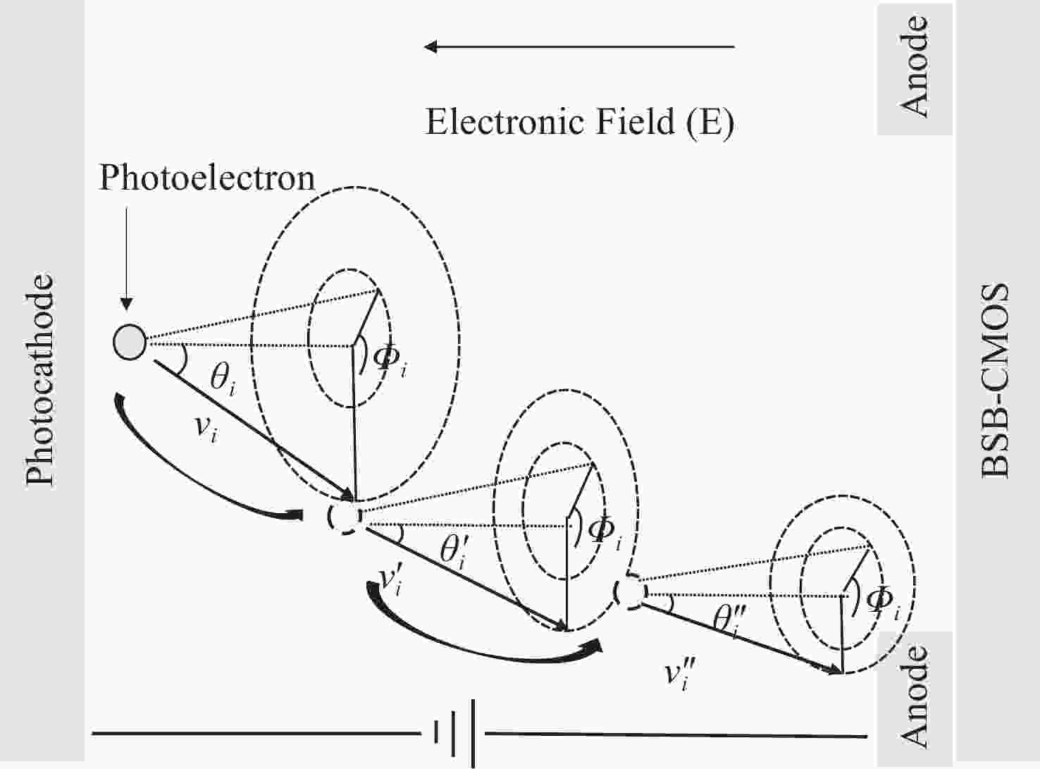
图 1 电场作用下电子运动轨迹变化示意图
Figure 1. Schematic diagram of changes in a photoelectron trajectory caused by the electric field
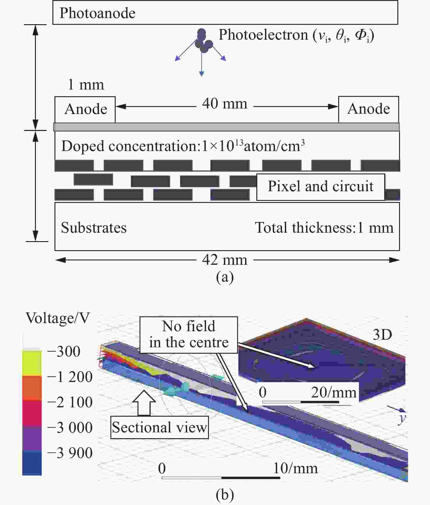
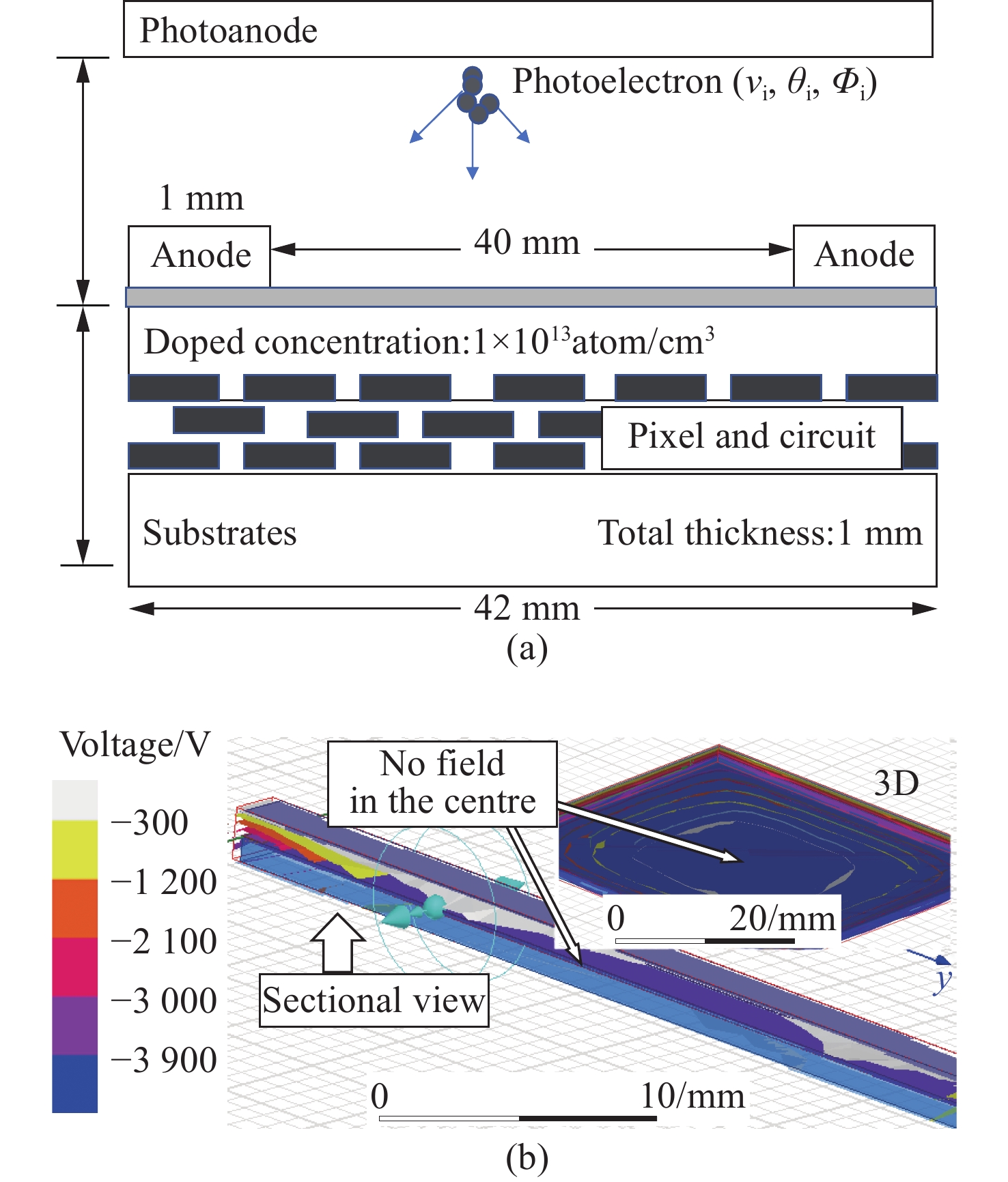
图 2 (a) 光电阴极与BSB-CMOS间的等势面不平行时EBCMOS近贴聚焦结构模型示意图及(b) 光电阴极与BSB-CMOS之间的电场分布模拟图
Figure 2. (a) Schematic diagram of the EBCMOS model with the proximity focusing structure when the equipotential surfaces between the photocathode and BSB-CMOS are not parallel and (b) electrostatic distribution between the photocathode and BSB-CMOS
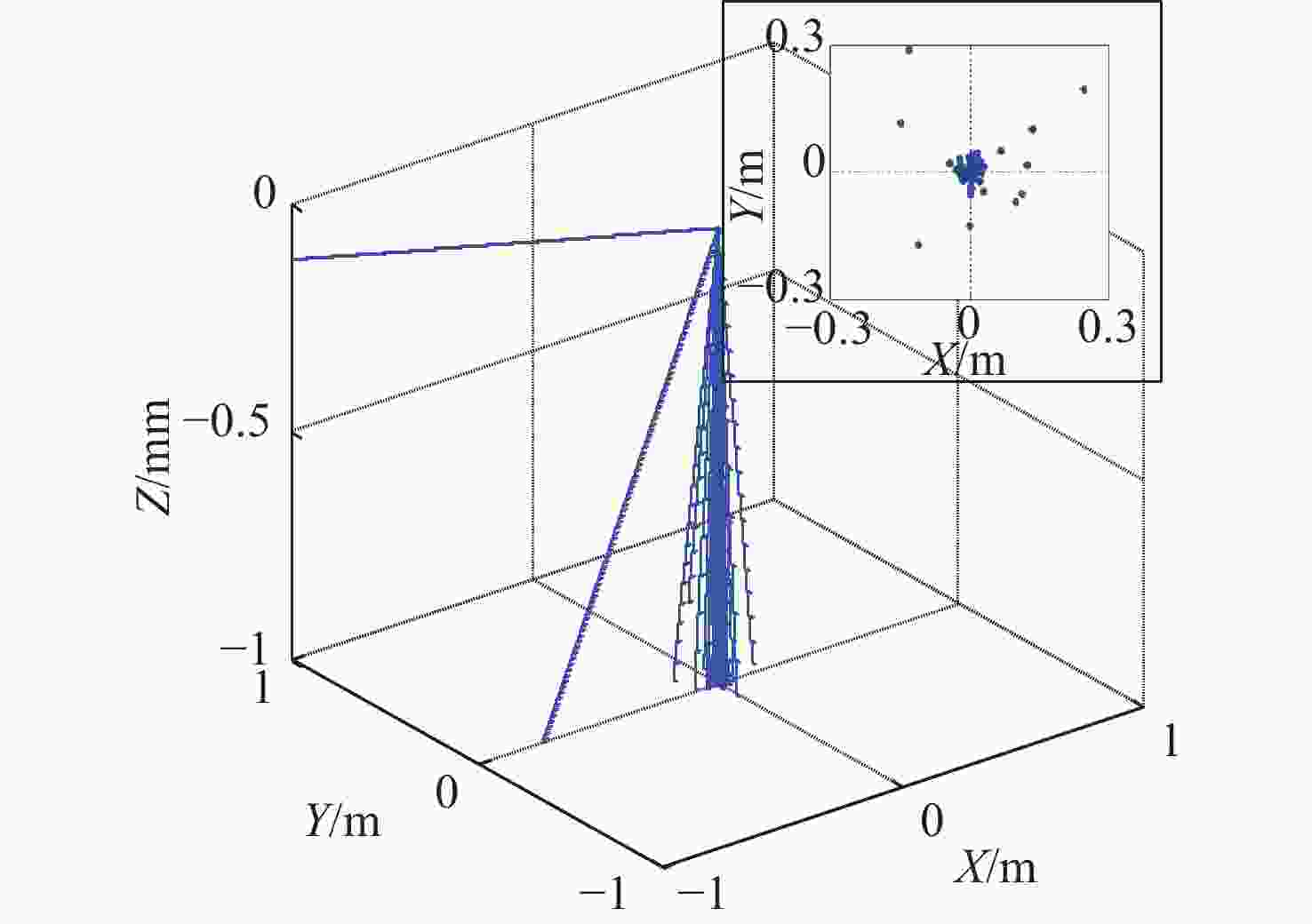
图 3 无电场时的电子运动轨迹模拟图。内图为轰击BSB-CMOS表面的光电子分布图(扩散范围超过0.1 mm2)
Figure 3. Simulation of electron trajectories in the absence of electric fields. Inset figure is the distribution diagram of photoelectrons bombarding the surface of BSB-CMOS (scattered over an area exceeding 0.1 mm2)
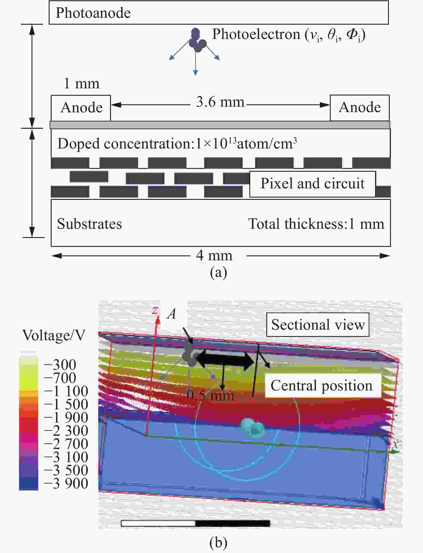
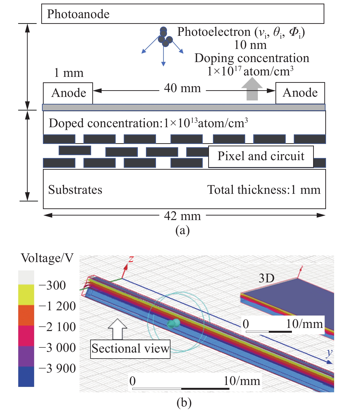
图 4 (a)光电阴极与BSB-CMOS间的等势面部分平行时EBCMOS近贴聚焦结构模型示意图及 (b)光电阴极与BSB-CMOS之间的电场分布模拟图
Figure 4. (a) Schematic diagram of the EBCMOS model with the proximity focusing structure when the equipotential surfaces between the photocathode and BSB-CMOS are partially parallel and (b) electrostatic distribution between the photocathode and BSB-CMOS
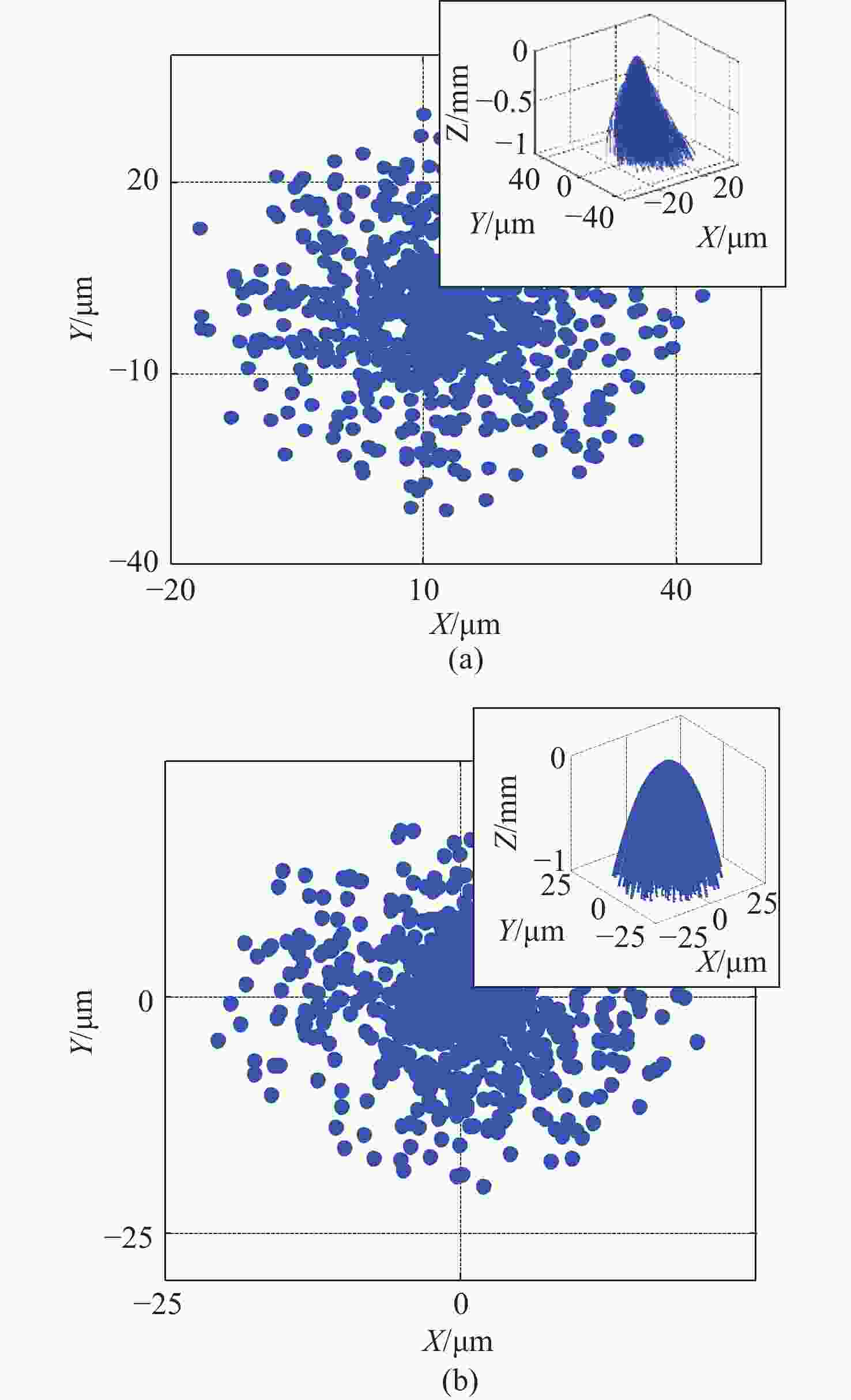
图 5 BSB-CMOS表面入射光电子分布图。(a)图4(b)中A位置所产生的光电子;(b)光电阴极表面中心位置所产生的光电子(内图:电子运动轨迹的三维模拟图)
Figure 5. Distribution diagram of photoelectrons bombarding the surface of BSB-CMOS. (a) Photoelectrons generated at the position A shown in Figure 4(b); (b) photoelectrons generated at the center of photocathode surface. (Inset figures: 3-D simulation diagram of electron trajectories)
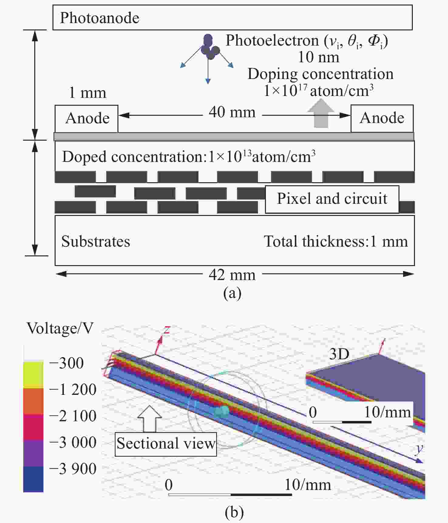
图 6 (a)光电阴极与BSB-CMOS间的等势面平行时EBCMOS近贴聚焦结构模型示意图及 (b)光电阴极与BSB-CMOS之间的电场分布模拟图
Figure 6. (a) Schematic diagram of the EBCMOS model with the proximity focusing structure when the equipotential surfaces between the photocathode and the BSB-CMOS are parallel and (b) electrostatic distribution between the photocathode and BSB-CMOS
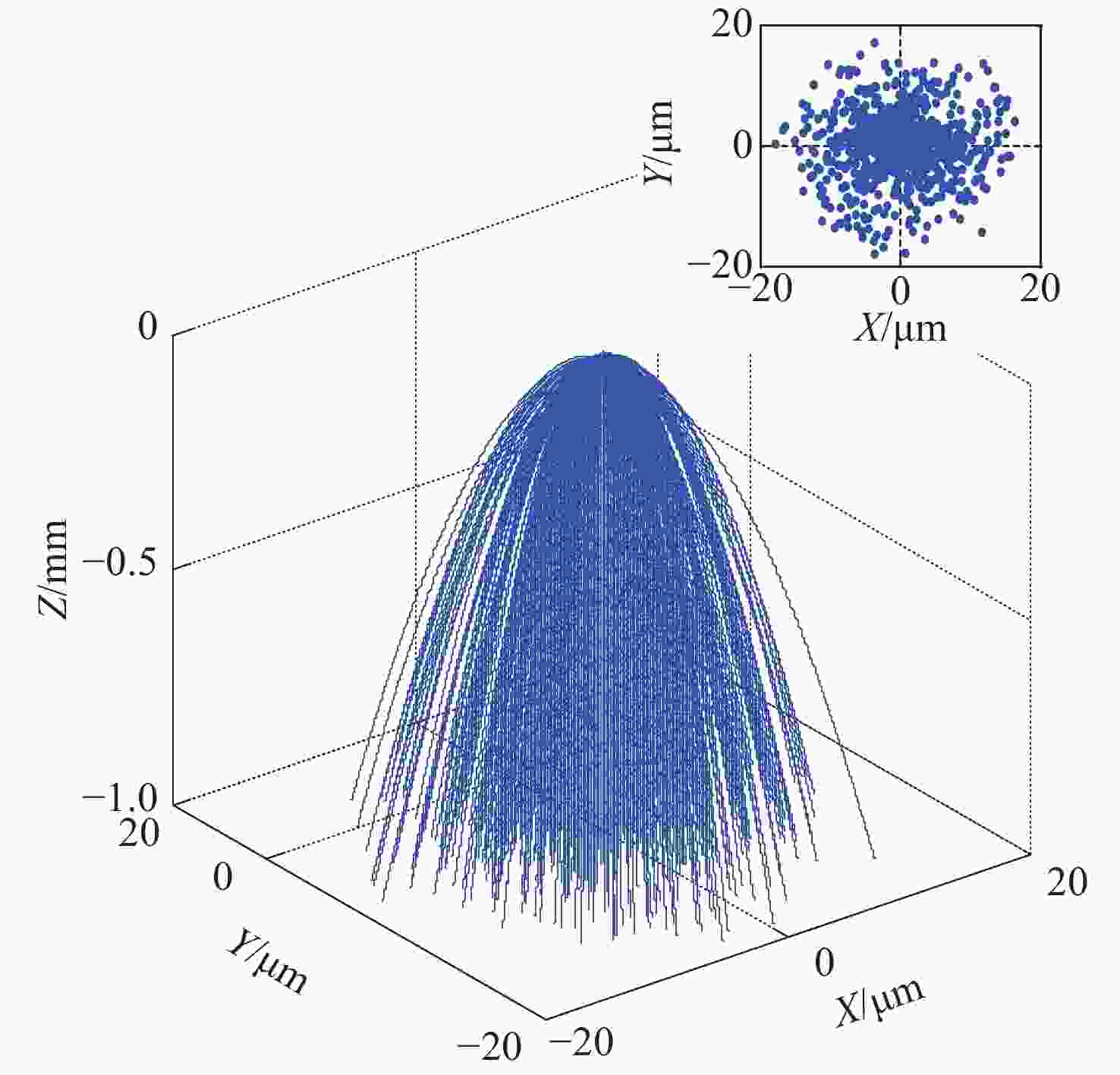
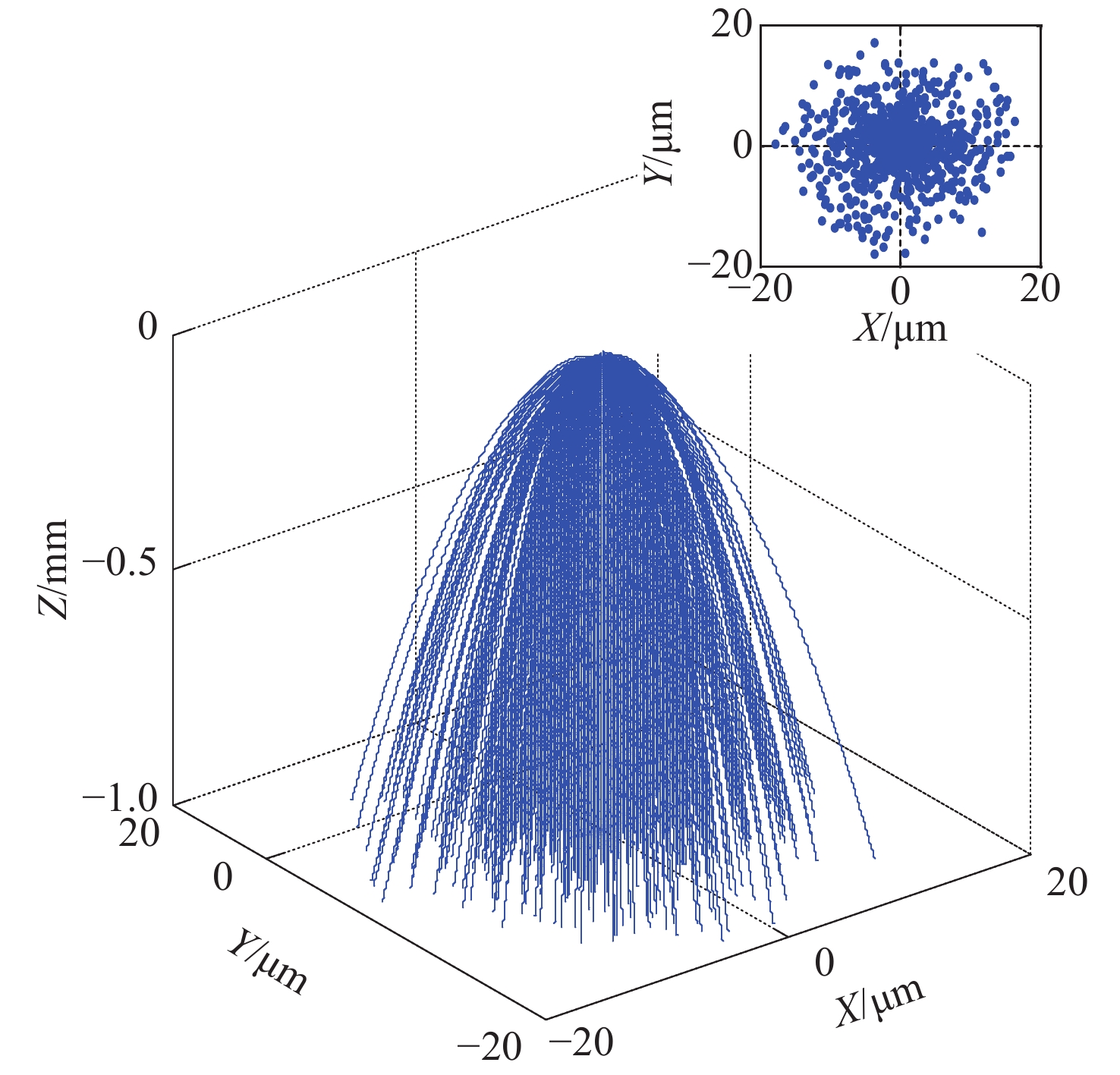
图 7 电子运动轨迹三维模拟图。内图为BSB-CMOS表面入射光电子分布图(扩散形成直径约为30 µm的圆)
Figure 7. 3D simulation diagram of electron trajectories. Inset figure is the distribution of photoelectrons bombarding the surface of BSB-CMOS (scattered into a circle with diameter of approximate 30 µm)
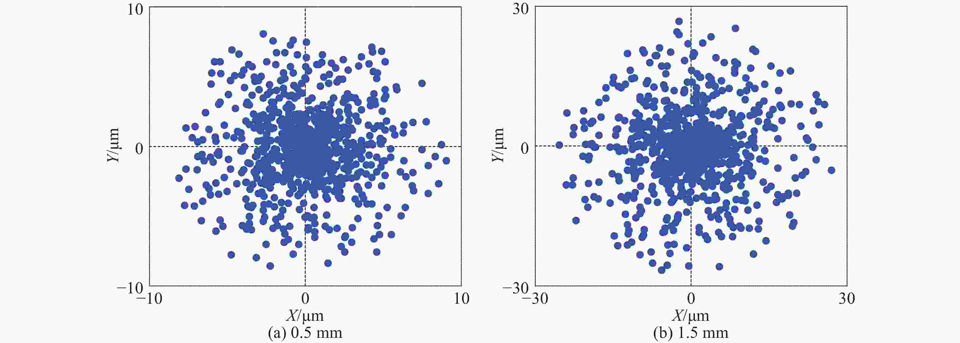
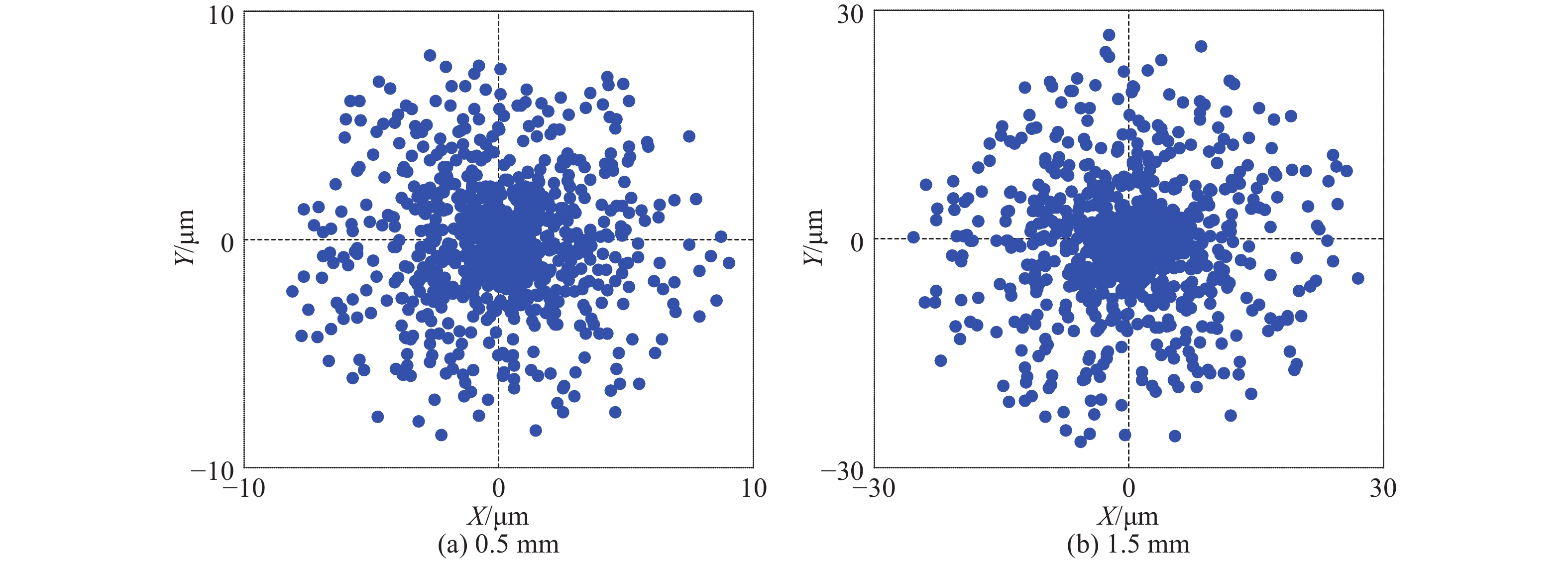
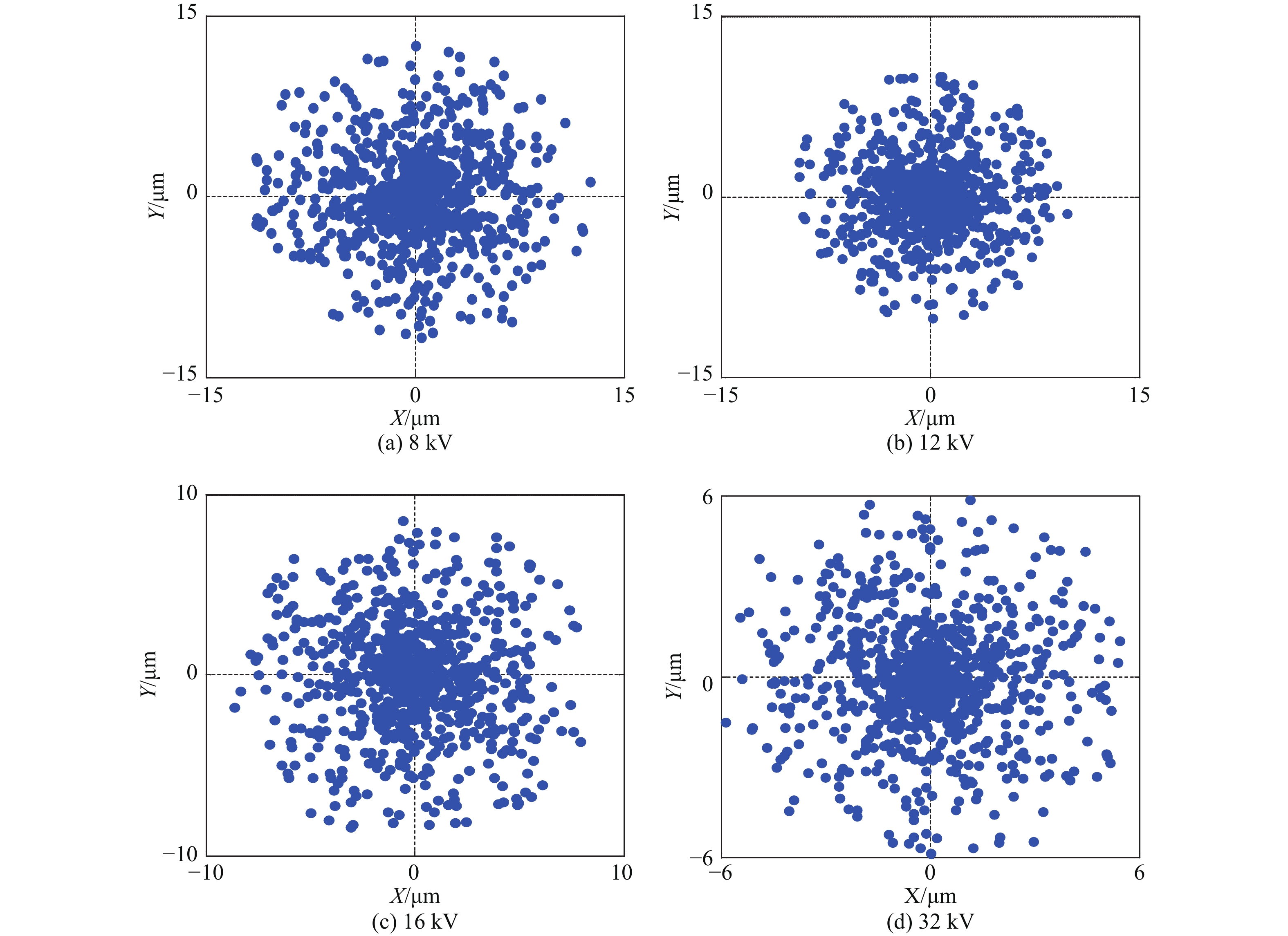
图 8 光电阴极与BSB-CMOS间距不同时,BSB-CMOS表面入射光电子分布图
Figure 8. Distribution diagrams of photoelectrons bombarding the surface of BSB-CMOS at different distances between photocathode and BSB-CMOS
-
[1] 金伟其, 陶禹, 石峰, 等. 微光视频器件及其技术的进展[J]. 红外与激光工程,2015,44(11):3167-3176. doi: 10.3969/j.issn.1007-2276.2015.11.001JIN W Q, TAO Y, SHI F, et al. Progress of low level light video technology[J]. Infrared and Laser Engineering, 2015, 44(11): 3167-3176. (in Chinese) doi: 10.3969/j.issn.1007-2276.2015.11.001 [2] 郭晖, 向世明, 田民强. 微光夜视技术发展动态评述[J]. 红外技术,2013,35(2):63-68.GUO H, XIANG SH M, TIAN M Q. A review of the development of low-light night vision technology[J]. Infrared Technology, 2013, 35(2): 63-68. (in Chinese) [3] QI L, JUST F, LEUCHS G, et al. Autonomous absolute calibration of an ICCD camera in single-photon detection regime[J]. Optics Express, 2016, 24(23): 26444-26453. doi: 10.1364/OE.24.026444 [4] TORR M R, TORR D G, BAUM R, et al. Intensified-CCD focal plane detector for space applications: a second generation[J]. Applied Optics, 1986, 25(16): 2768-2777. doi: 10.1364/AO.25.002768 [5] BRUGIÈRE T, MAYER F, FEREYRE P, et al. First measurement of the in-pixel electron multiplying with a standard imaging CMOS technology: Study of the EMCMOS concept[J]. Nuclear Instruments and Methods in Physics Research Section A:Accelerators,Spectrometers,Detectors and Associated Equipment, 2015, 787: 336-339. doi: 10.1016/j.nima.2015.01.065 [6] ROBBINS M S, HADWEN B J. The noise performance of electron multiplying charge-coupled devices[J]. IEEE Transactions on Electron Devices, 2003, 50(5): 1227-1232. doi: 10.1109/TED.2003.813462 [7] HIRVONEN L M, JIGGINS S, SERGENT N, et al. Photon counting imaging with an electron-bombarded CCD: Towards wide-field time-correlated single photon counting (TCSPC)[J]. Nuclear Instruments and Methods in Physics Research Section A:Accelerators,Spectrometers,Detectors and Associated Equipment, 2015, 787: 323-327. doi: 10.1016/j.nima.2015.01.031 [8] 朱敏, 田进寿, 温文龙, 等. 基于电子轰击式CCD的大动态条纹相机研究[J]. 物理学报,2015,64(9):098501. doi: 10.7498/aps.64.098501ZHU M, TIAN J SH, WEN W L, et al. Research on large dynamic range streak camera based on electron-bombarded CCD[J]. Acta Physica Sinica, 2015, 64(9): 098501. (in Chinese) doi: 10.7498/aps.64.098501 [9] HIRVONEN L M, SUHLING K. Photon counting imaging with an electron-bombarded pixel image sensor[J]. Sensors, 2016, 16(5): 617. doi: 10.3390/s16050617 [10] 刘虎林, 王兴, 田进寿, 等. 高分辨紫外电子轰击互补金属氧化物半导体器件的实验研究[J]. 物理学报,2018,67(1):014209. doi: 10.7498/aps.67.20171729LIU H L, WANG X, TIAN J SH, et al. High resolution electron bombareded complementary metal oxide semiconductor sensor for ultraviolet detection[J]. Acta Physica Sinica, 2018, 67(1): 014209. (in Chinese) doi: 10.7498/aps.67.20171729 [11] AEBI V W, COSTELLO K A, ARCUNI P W, et al.. EBAPS: Next generation, low power, digital night vision[C]. Presented at the OPTRO 2005 International Symposium, OPTRO, 2005: 1-10. [12] AEBI V W, BOYLE J J. Electron bombarded active pixel sensor: US, 6285018B1[P]. 2001-09-04. [13] BARBIER R, DEPASSE P, BAUDOT J, et al.. First Results from the development of a new generation of hybrid photon detector: EBCMOS[C]. Proceedings of the 10th Conference on Astroparticle, Particle and Space Physics, Detectors and Medical Physics Applications, World Scientific, 2008: 23-27. [14] CAJGFINGER T, DOMINJON A, BARBIER R. Single photon detection and localization accuracy with an EBCMOS camera[J]. Nuclear Instruments and Methods in Physics Research Section A:Accelerators,Spectrometers,Detectors and Associated Equipment, 2015, 787: 176-181. [15] DOMINJON A, CHABANAT E, DEPASSE P, et al.. LUSIPHER large-scale ultra-fast single photo-electron tracker[C]. 2009 IEEE Nuclear Science Symposium Conference Record (NSS/MIC), IEEE, 2009: 1527-1531. [16] 宋德, 朴雪, 拜晓锋, 等. 近贴型像增强器中微通道板输入端电场模拟研究[J]. 红外与激光工程,2015,44(10):2981-2986. doi: 10.3969/j.issn.1007-2276.2015.10.019SONG D, PIAO X, BAI X F, et al. Simulation research of electrostatic field of MCP input in proximity image intensifier[J]. Infrared and Laser Engineering, 2015, 44(10): 2981-2986. (in Chinese) doi: 10.3969/j.issn.1007-2276.2015.10.019 [17] 宋德, 石峰, 李野. 基底均匀掺杂下EBAPS电荷收集效率的模拟研究[J]. 红外与激光工程,2016,45(2):0203002. doi: 10.3788/irla201645.0203002SONG D, SHI F, LI Y. Simulation of charge collection efficiency for EBAPS with uniformly doped substrate[J]. Infrared and Laser Engineering, 2016, 45(2): 0203002. (in Chinese) doi: 10.3788/irla201645.0203002 [18] BARBIER R, CAJGFINGER T, CALABRIA P, et al. A single-photon sensitive ebCMOS camera: The LUSIPHER prototype[J]. Nuclear Instruments and Methods in Physics Research Section A:Accelerators,Spectrometers,Detectors and Associated Equipment, 2011, 648(1): 266-274. -

 下载:
下载:


计量
- 文章访问数: 2346
- HTML全文浏览量: 716
- PDF下载量: 128
- 被引次数: 0
