


Fabrication and characterization of ultra-thin GaN-based LED freestanding membrane
doi: 10.37188/CO.2019-0192
-
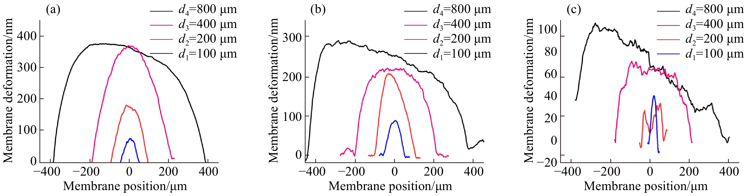
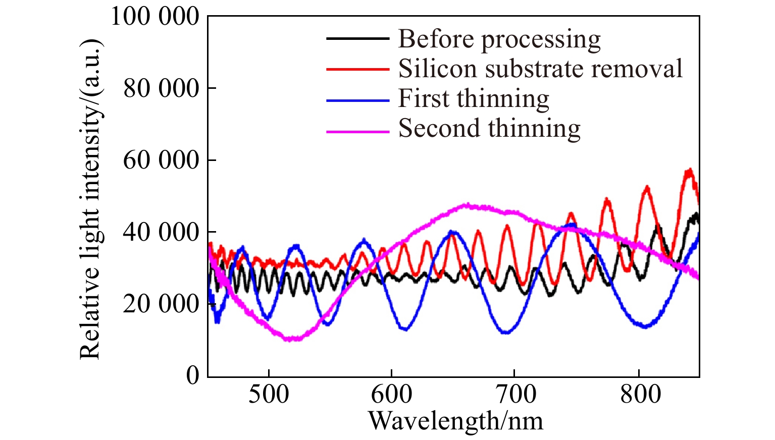
摘要: 为了便于导出LED有源层的出射光,本文研究了亚微米厚度LED悬空薄膜的工艺实现、形貌表征和光学性能表征。采用光刻工艺、深反应离子刻蚀技术和快速原子束刻蚀技术相结合的背后工艺,实现了基于硅基氮化镓晶圆的超薄氮化镓基LED悬空薄膜器件。本文利用白光干涉仪观察制备的超薄LED悬空薄膜的变形程度,发现薄膜变形大小与薄膜直径呈正相关,而与薄膜厚度呈负相关。薄膜变形大小低至纳米级,并且为中央凸起边缘平滑的拱形变形。通过反射谱测试发现未经加工的硅基氮化镓晶圆的反射模式数较多,而LED悬空薄膜的反射模式数大幅度减少,且反射谱整体光强明显提高。在光致发光测试中,发现由于应力释放,悬空薄膜的出射光峰值较硅基氮化镓晶圆出现了8.2 nm的蓝移,并且从背面也可以探测到移除了大部分外延层的超薄LED悬空薄膜有明显的出射光。这表明悬空薄膜在光致发光情况下更有利于导出发射光。本研究工作实现了厚度小、面积大、总体变形程度小、光学性能优良的LED悬空薄膜,为氮化镓基LED器件在光微机电领域的应用开辟了新的途径。Abstract: In order to deliver the emergent light of Light Emitting Diode (LED) active layer easily, we studied the fabrication process, morphological characterization and optical characterization of submicron-level LED freestanding membrane. We prepared ultra-thin GaN-based LED freestanding membrane based on GaN-on-silicon wafer by using the backside process with photolithography, deep reactive ion etching and fast atom beam etching. Through a white light interferometer, we found that the deformation of the prepared ultra-thin LED freestanding membrane is positively correlated with the diameter of membrane, but negatively correlated with the thickness of membrane. The deformation as a whole is a smooth nanoscale arch deformation. Through the reflection spectrum test, we found that the number of reflection modes of LED freestanding membrane is much smaller than that of unprocessed silicon-based gallium nitride wafer and that the overall light intensity of reflection spectrum of the membrane is obviously improved. In the photoluminescence test, we found that due to the stress release, the emergent spectral peak of LED freestanding membrane has a blue shift of 8.2 nm compared with silicon-based gallium nitride wafer. Moreover, obvious outgoing light can be detected on the backside of the ultra-thin LED freestanding membrane with most of epitaxial layer removed. It demonstrates that LED freestanding membrane is more beneficial to deliver the emitted light in the photoluminescence test. In this study, the LED freestanding membrane with small thickness, large area, small deformation and excellent optical properties has been realized. It provides a new way for the application of GaN-based LED in the field of Micro-Optical Mechanic Electronic System (MOMES).
-
Key words:
- gallium nitride /
- freestanding membrane /
- LED /
- reflection spectrum /
- photoluminescence
-
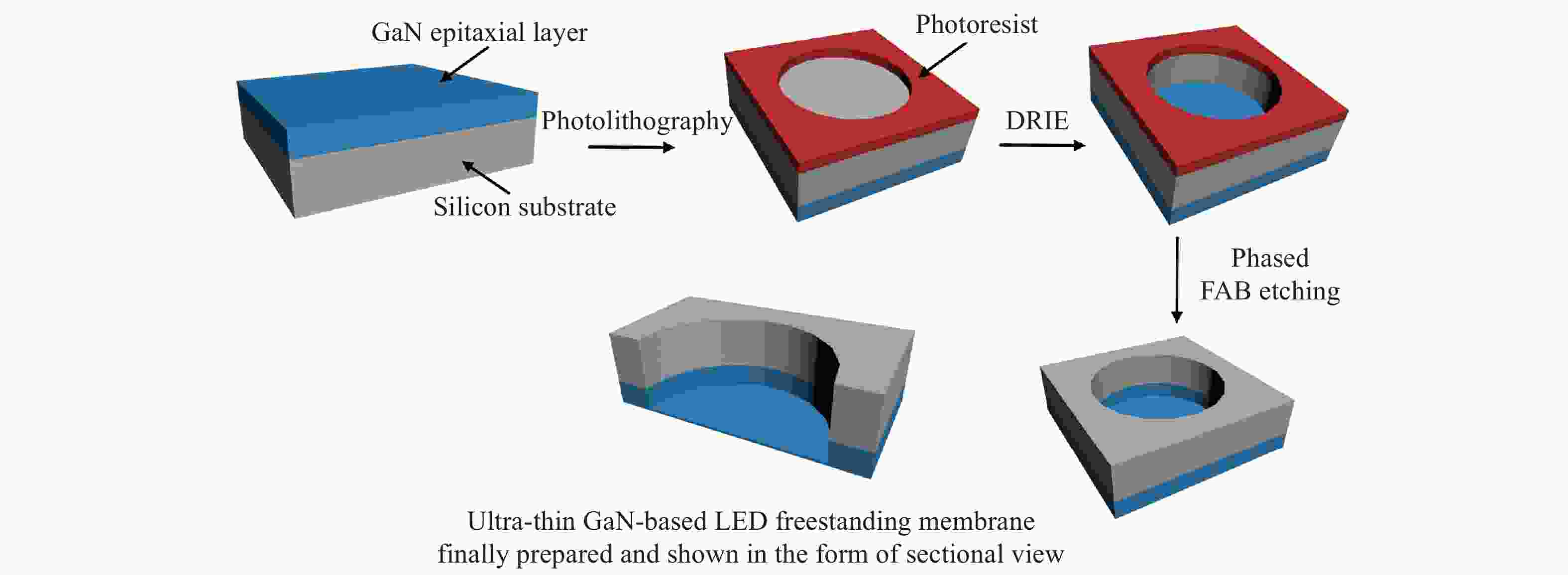
图 1 超薄氮化镓基LED悬空薄膜工艺流程图
Figure 1. Fabrication process of ultra-thin GaN-based LED freestanding membrane
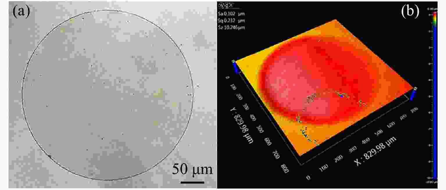
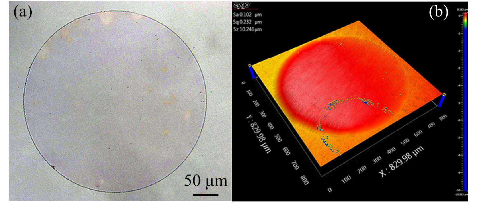
图 2 剥离硅衬底的直径为800 μm的LED悬空薄膜的 (a)正面光镜图及(b)白光干涉仪获得的悬空薄膜三维变形图
Figure 2. LED freestanding membrane with 800 μm diameter after removing silicon substrate. (a) Top-view optical microscope image, (b) 3D deformation image obtained by white light interferometer
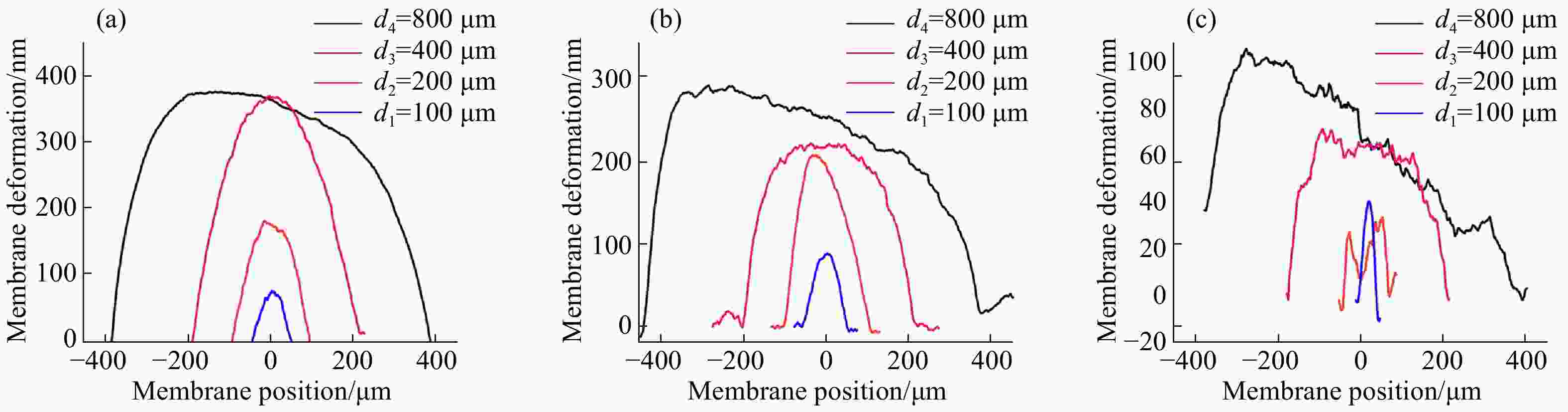
图 3 具有不同直径的LED悬空薄膜的变形情况。 (a)掏空硅衬底,(b)背后减薄一次,(c)背后减薄两次
Figure 3. Deformations of LED freestanding membranes with different diameters. (a) Removing silicon substrate, (b) thinning the backside once, (c) thinning the backside twice
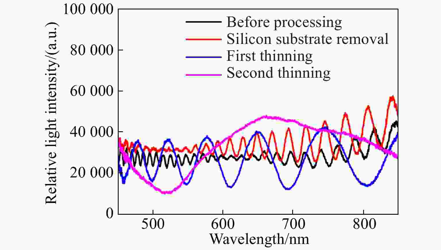
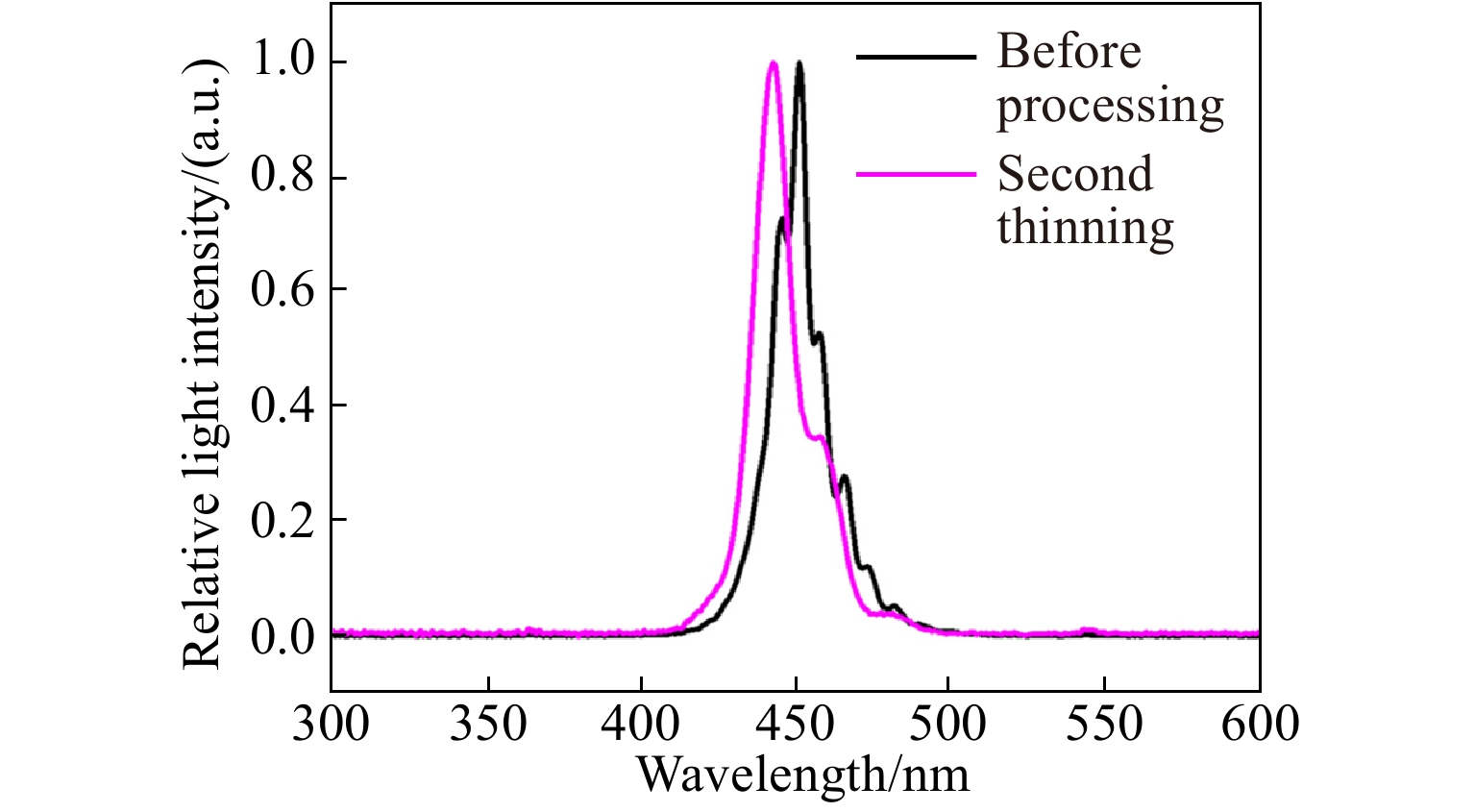
图 4 具有不同厚度LED悬空薄膜的反射谱
Figure 4. Reflectance spectra of LED freestanding membranes with different thicknesses
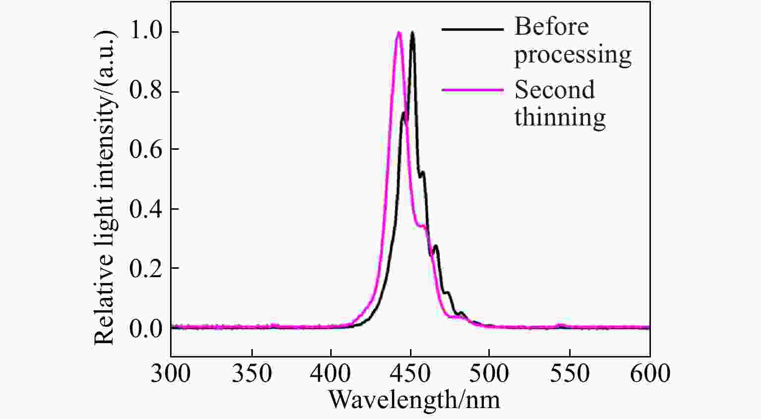
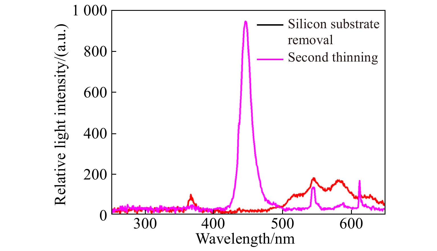
图 5 正面激发下不同厚度LED悬空薄膜的光致发光谱
Figure 5. Photoluminescence spectra of LED freestanding membranes with different thicknesses under front excitation
-
[1] PEARTON S J, ZOLPER J C, SHUL R J, et al. GaN: processing, defects, and devices[J]. Journal of Applied Physics, 1999, 86(1): 1-78. [2] ZHANG Y H, DADGAR A, PALACIOS T. Gallium nitride vertical power devices on foreign substrates: a review and outlook[J]. Journal of Physics D:Applied Physics, 2018, 51(27): 273001. doi: 10.1088/1361-6463/aac8aa [3] NAKAMURA S, PEATRON S, FASOL G. The Blue Laser Diode: the Complete Story[M]. 2nd ed. Berlin: Springer, 2000. [4] ALHASSAN A I, YOUNG E C, ALYAMANI A Y, et al. Reduced-droop green III-nitride light-emitting diodes utilizing GaN tunnel junction[J]. Applied Physics Express, 2018, 11(4): 042101. doi: 10.7567/APEX.11.042101 [5] LI B, REN Y, CHANG B K. Stability of gradient-doping GaN photocathode[J]. Chinese Optics, 2018, 11(4): 677-683. (in Chinese) doi: 10.3788/co.20181104.0677 [6] MORELLE C, THÉRON D, DERLUYN J, et al. Gallium nitride MEMS resonators: how residual stress impacts design and performances[J]. Microsystem Technologies, 2018, 24(1): 371-377. doi: 10.1007/s00542-017-3293-0 [7] YANG ZH CH, LÜ J N, YAN G ZH, et al. Fabrication of GaN-based MEMS structures using dry-etch technique[J]. Nanotechnology and Precision Engineering, 2011, 9(1): 78-82. doi: 10.3969/j.issn.1672-6030.2011.01.015 [8] LI X, SHI ZH, HE SH M, et al. MEMS-tunable Ⅲ-nitride grating on silicon substrate[J]. Optics and Precision Engineering, 2014, 22(11): 2945-2949. (in Chinese) doi: 10.3788/OPE.20142211.2945 [9] TABATABA-VAKILI F, ROLAND I, TRAN T M, et al. Q factor limitation at short wavelength (around 300 nm) in III-nitride-on-silicon photonic crystal cavities[J]. Applied Physics Letters, 2017, 111(13): 131103. doi: 10.1063/1.4997124 [10] PRABASWARA A, MIN J W, ZHAO CH, et al. Direct growth of III-nitride nanowire-based yellow light-emitting diode on amorphous quartz using thin Ti interlayer[J]. Nanoscale Research Letters, 2018, 13(1): 41. doi: 10.1186/s11671-018-2453-1 [11] LI T P, ZHAO G ZH, LU T P, et al. Effect of Undoped GaN layer thickness on the wavelength uniformity of GaN based blue LEDs[J]. Chinese Journal of Luminescence, 2017, 38(9): 1198-1204. (in Chinese) doi: 10.3788/fgxb20173809.1198 [12] ZHOU ZH Y, YANG K, HUANG Y M, et al. Recombination Process in InGaN/GaN MQW LED on Silicon with δ-Si Doped n-GaN Layer[J]. Chinese Journal of Luminescence, 2018, 39(12): 1722-1729. (in Chinese) doi: 10.3788/fgxb20183912.1722 [13] CHARLES M, MRAD M, KANYANDEKWE J, et al. Extraction of stress and dislocation density using in-situ curvature measurements for AlGaN and GaN on silicon growth[J]. Journal of Crystal Growth, 2019, 517: 64-67. doi: 10.1016/j.jcrysgro.2019.04.014 [14] WANG K J, WANG A Q, JI Q B, et al. Epitaxy of GaN in high aspect ratio nanoscale holes over silicon substrate[J]. Applied Physics Letters, 2017, 111(25): 252101. doi: 10.1063/1.5002529 [15] ISHIKAWA H, ASANO K, ZHANG B, et al. Improved characteristics of GaN-based light-emitting diodes by distributed Bragg reflector grown on Si[J]. Physica Status Solidi (A) , 2004, 201(12): 2653-2657. [16] ISHIKAWA H, JIMBO T, EGAWA T. GaInN light emitting diodes with AlInN/GaN distributed Bragg reflector on Si[J]. Physica Status Solidi C, 2008, 5(6): 2086-2088. doi: 10.1002/pssc.200778441 [17] ZHANG B J, EGAWA T, ISHIKAWA H, et al. Thin-film InGaN multiple-quantum-well light-emitting diodes transferred from Si (111) substrate onto copper carrier by selective lift-off[J]. Applied Physics Letters, 2005, 86(7): 071113. doi: 10.1063/1.1863412 [18] CHEN T F, WANG Y Q, XIANG P, et al. Crack-free InGaN multiple quantum wells light-emitting diodes structures transferred from Si (111) substrate onto electroplating copper submount with embedded electrodes[J]. Applied Physics Letters, 2012, 100(24): 241112. doi: 10.1063/1.4729414 [19] LUO R H, RAO W T, CHEN T F, et al. Vertical InGaN multiple quantum wells light-emitting diodes structures transferred from Si (111) substrate onto electroplating copper submount with through-holes[J]. Japanese Journal of Applied Physics, 2012, 51(1R): 012101. doi: 10.7567/JJAP.51.012101 [20] HUANG B B, XIONG CH B, TANG Y W, et al. Changes of stress and luminescence properties in GaN-based LED films before and after transferring the films to a flexible layer on a submount from the silicon epitaxial substrate[J]. Acta Physica Sinica, 2015, 64(17): 177804. (in Chinese) doi: 10.7498/aps.64.177804 -

 下载:
下载:


计量
- 文章访问数: 2656
- HTML全文浏览量: 1314
- PDF下载量: 119
- 被引次数: 0
