


Investigation of damage rules in silicon PIN photodiodes under xenon lamp irradiation
-
摘要:
为研究硅PIN光电二极管(简称PIN管)在氙灯辐照下的性能退化规律和损伤机理,本研究定义了PIN管的探测能力,搭建了50 kW氙灯损伤实验平台,以S5106型PIN管为对象,通过实时监测其输出光电流和表面温度的变化,探究了PIN管损伤时探测能力退化的影响因素和损伤阈值特性。基于一维热扩散理论建立了PIN管的损伤阈值模型,通过与实验阈值结果进行对比,验证了模型的准确性。根据探测能力是否可恢复,将PIN管损伤分为软损伤和硬损伤。软损伤时探测能力与辐照时间、表面温度均呈非线性负相关关系;硬损伤时辐照度阈值与辐照时间的平方根成反比,与损伤阈值模型一致,其损伤阈值对应的最小辐照度约为6.6 W/cm2(对应辐照时间约为382 s),此时表面温度范围为(385.77±4.16) °C。理论分析表明,软损伤源于热效应导致的载流子迁移率下降及漏电流增大,硬损伤源于热效应导致的光学窗口硅橡胶熔融开裂与PN结热失效。本研究明确了PIN管软损伤和硬损伤的影响因素及规律,并确定了其硬损伤阈值,为宽谱强光探测场景下PIN管的性能评估与防护设计提供了量化依据。
Abstract:This study investigates the performance degradation and underlying damage mechanisms of silicon PIN photodiodes under xenon lamp irradiation. To this end, detectivity is defined and operationalized. A 50 kW xenon lamp irradiation test platform was established, where the S5106-type silicon PIN photodiodes were selected as the representative test device. Real-time monitoring of output photocurrent and surface temperature enabled systematic analysis of the factors governing detectivity degradation, as well as characterization of the damage threshold. A damage threshold model for silicon PIN photodiodes was developed based on the one-dimensional heat diffusion equation. Model accuracy was verified by comparing with the experimentally measured threshold data. Silicon PIN photodiode damage was categorized into two regimes—soft damage and hard damage—based on the recoverability of detectivity. Under soft damage conditions, the detectivity of the device exhibited a nonlinear negative correlation with both irradiation time and surface temperature. The hard damage irradiance thresholds followed an inverse-square-root dependence on irradiation time, a trend fully consistent with the damage threshold model. Hard damage was observed at a minimum irradiance of approximately 6.6 W/cm2, corresponding to an irradiation time of about 382 s. Under this threshold condition, the surface temperature ranged within (385.77±4.16)°C. Theoretical analysis indicated that soft damage primarily arose from thermally induced degradation of carrier mobility and increased leakage current. Conversely, hard damage resulted from melting and cracking of the silicone rubber optical window, as well as thermally induced functional failure of the PN junction. The findings provide a quantitative basis for performance evaluation and protection design of silicon PIN photodiodes employed in broad-spectrum high-intensity optical detection scenarios.
-
Key words:
- silicon PIN photodiode /
- xenon lamp /
- broad-spectrum high-intensity light /
- damage rules /
- threshold /
- thermal effects
-
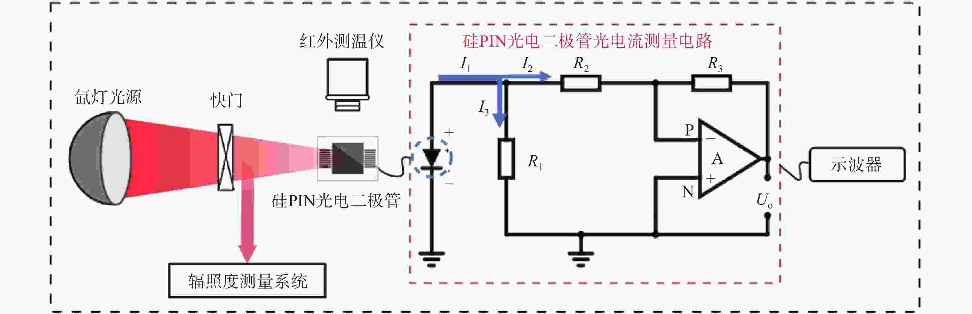
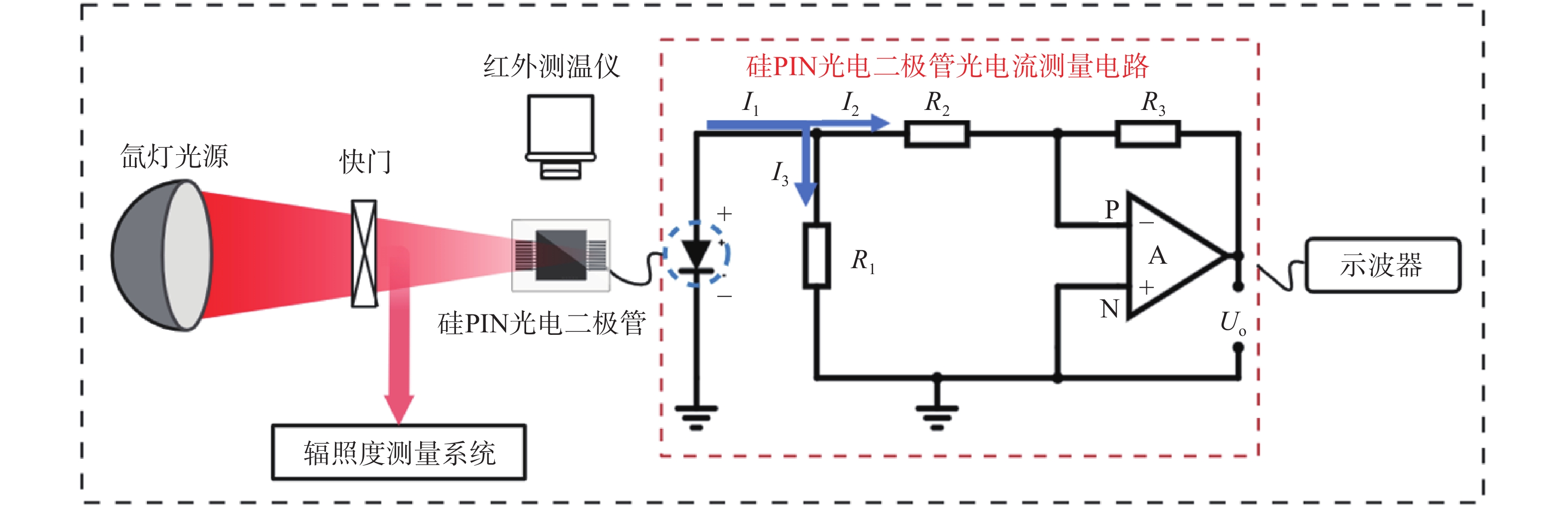
图 1 氙灯损伤平台及PIN管光电流测量电路示意图。图中I1为PIN管输出光电流,I2为流过反相输入端电阻R3的电流,I3为流过分流电阻R1的电流,Uo为运算放大器A的输出电压
Figure 1. Schematic diagram of Xenon lamp damage test platform and silicon PIN photodiode photocurrent measurement circuit. I1: photocurrent of silicon PIN photodiode; I2: current through inverting input resistor (R3); I3: current through shunt resistor (R1); Uₒ: output voltage of operational amplifier A
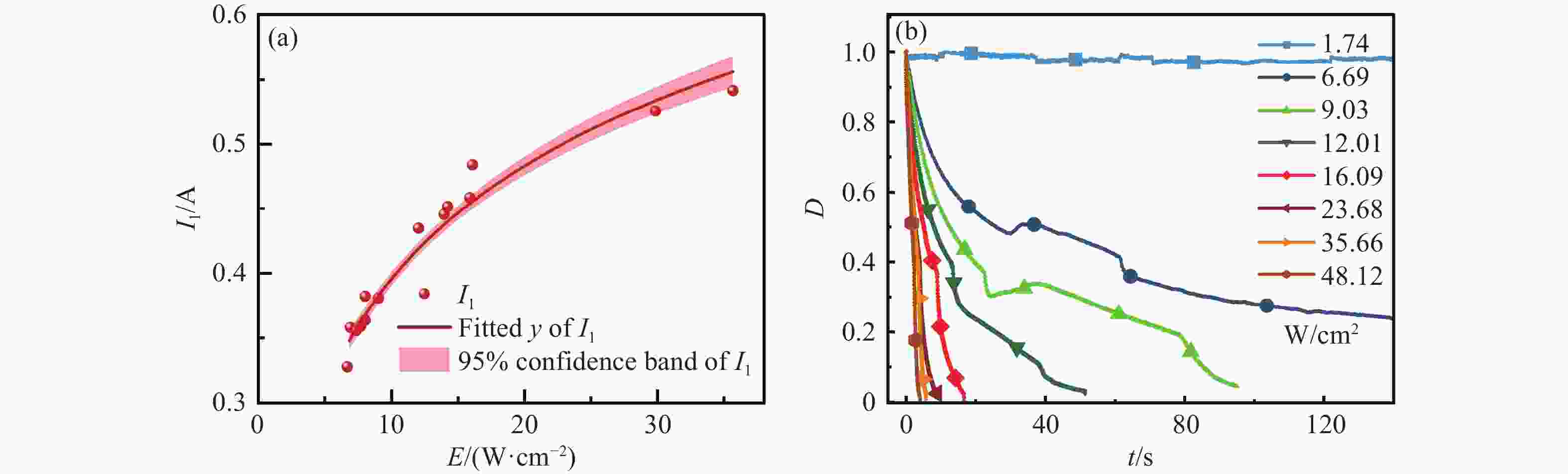
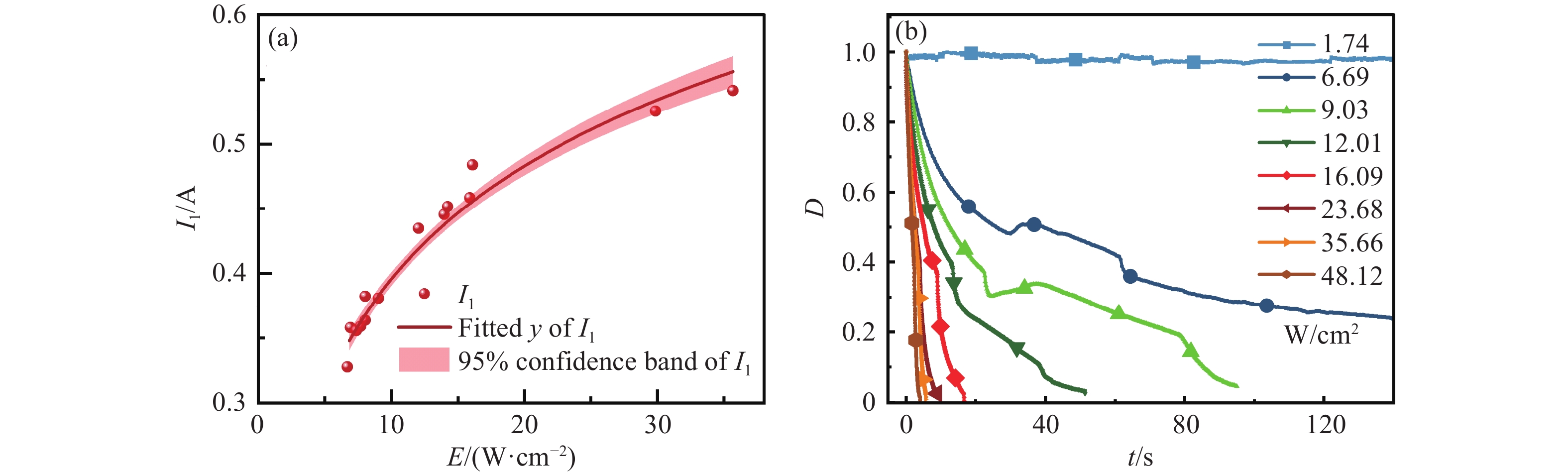
图 2 PIN管输出电流退化规律。(a)无损伤情况下,初始输出电流I1随辐照度E变化曲线。(b)不同辐照度E下,PIN管探测能力D随辐照时间t变化曲线
Figure 2. Output current degradation rules in the silicon PIN photodiode. (a) Initial output current (I1) versus irradiance (E) for the undamaged device. (b) Detectivity (D) versus irradiation time (t) at various irradiance levels (E)
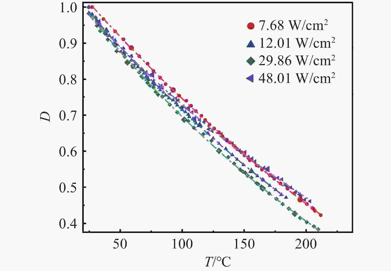
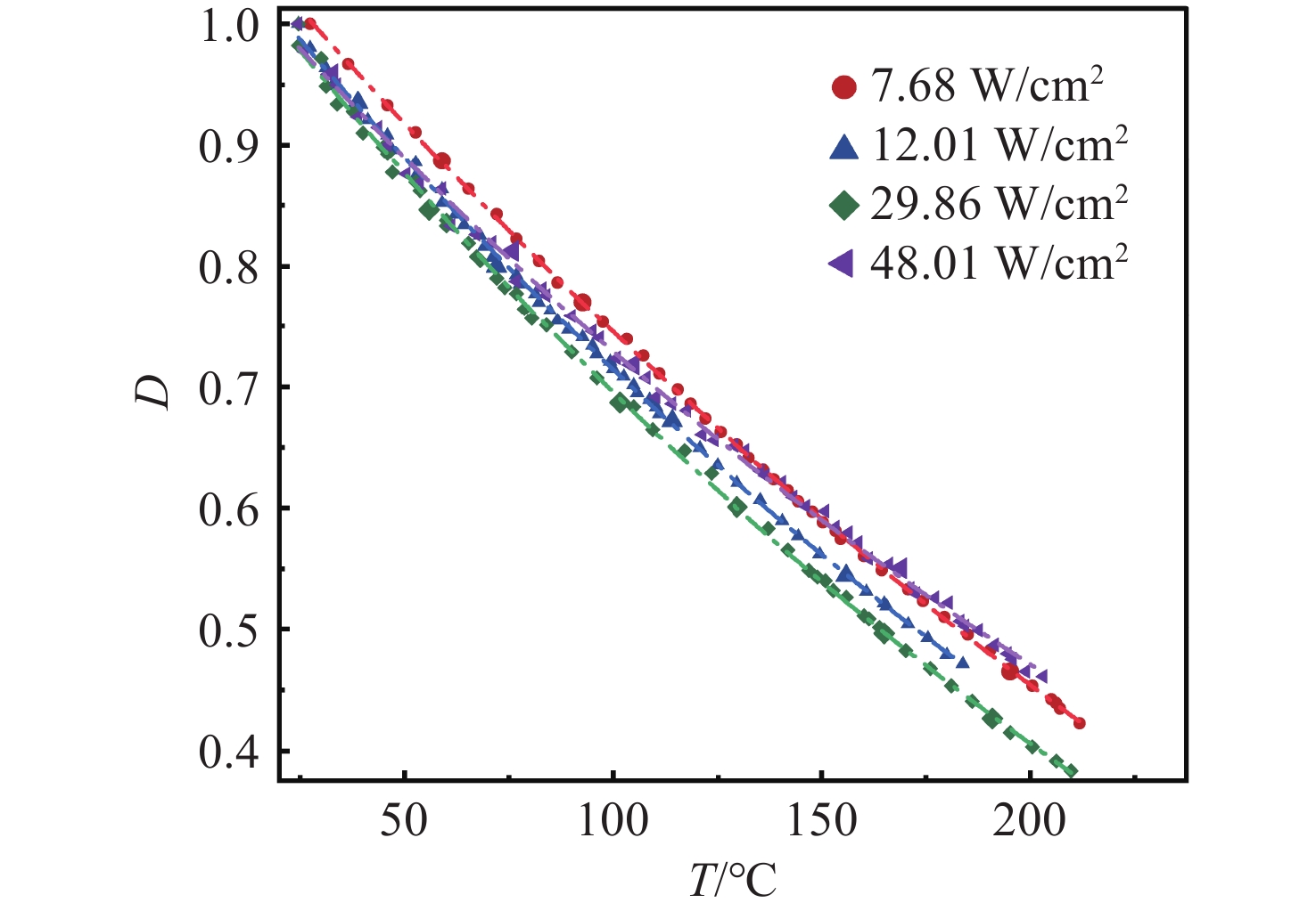
图 3 不同辐照度下,PIN管探测能力D随表面温度T变化曲线
Figure 3. Detectivity (D) versus surface temperature (T) at various irradiance levels
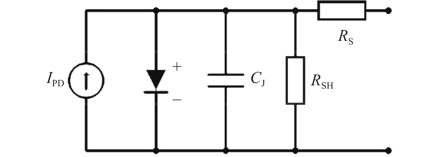
图 4 PIN管内部等效电路,其中IPD为光电流,CJ为等效电容,RSH为并联电阻,RS为串联电阻
Figure 4. Internal equivalent circuit of the silicon PIN photodiode. IPD: photocurrent; CJ: junction capacitance; RSH: shunt resistance; RS: series resistance
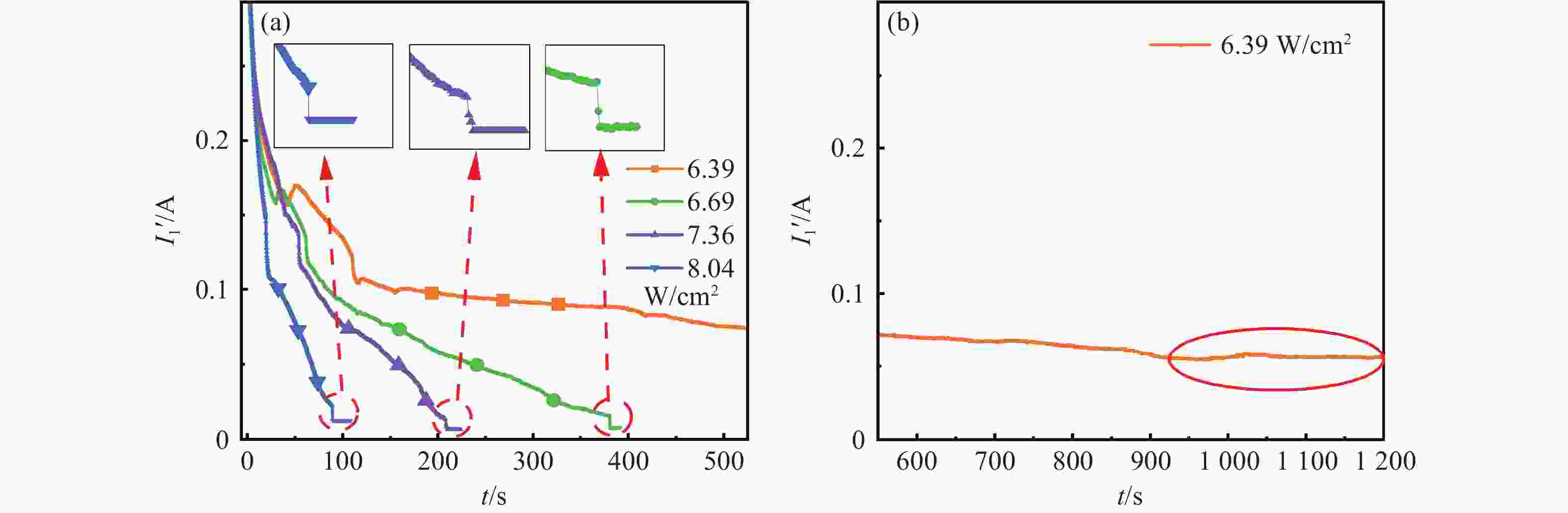
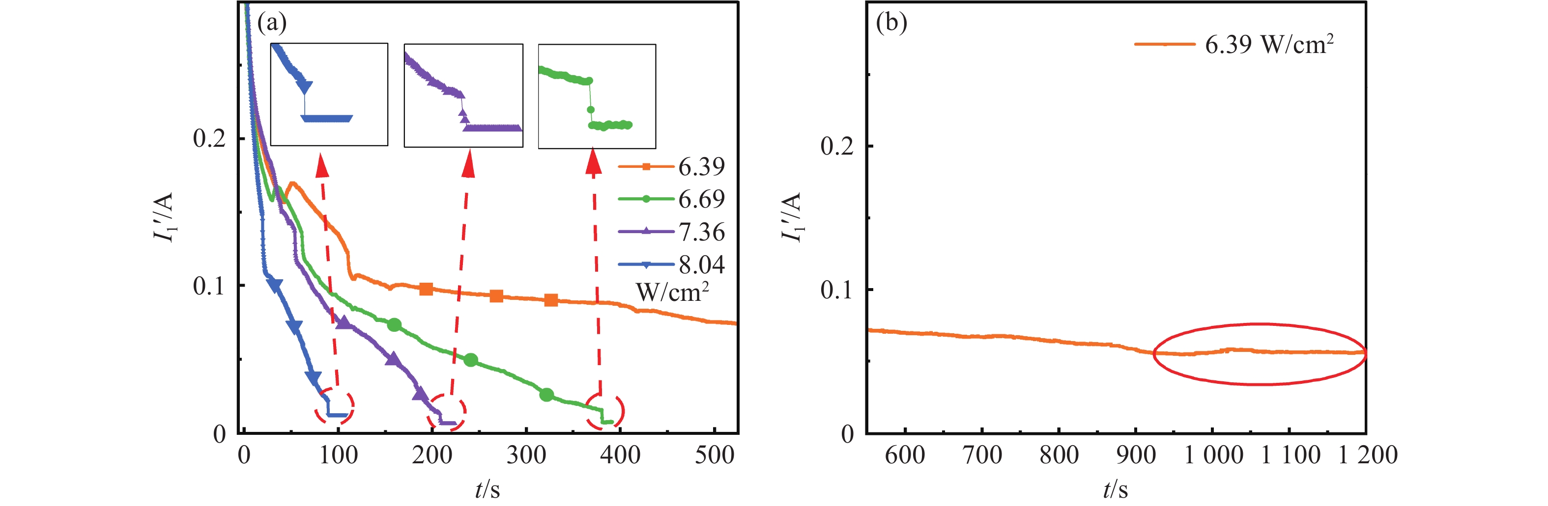
图 5 不同辐照度下,PIN管的I1′随时间变化情况。(a)PIN管发生硬损伤的I1′变化情况。(b)辐照度为6.39 W/cm2时,PIN管的I1′下降至稳定的情况
Figure 5. Variation of I1′ with time(t) under different irradiances. (a) Variation of I1′ under hard damage conditions in a silicon PIN photodiode. (b) Variation of I1′ of the silicon PIN photodiode decreasing to stability at an irradiance of 6.39 W/cm2
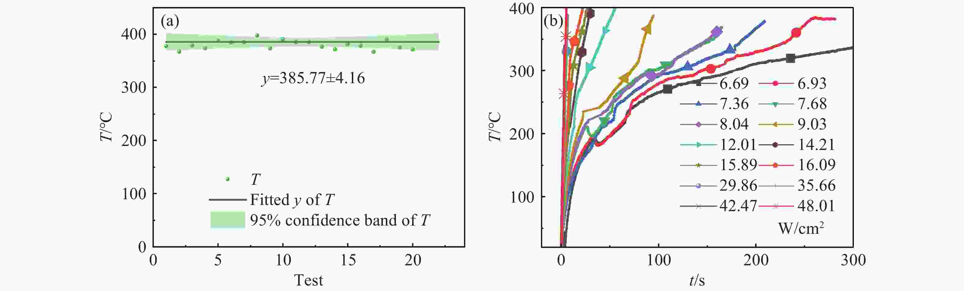
图 6 PIN管硬损伤表面温度变化情况。(a)不同辐照度实验中,硬损伤对应温度,横坐标为实验次序。(b)不同辐照度下,温度T随辐照时间t变化曲线
Figure 6. Variation of surface temperature with hard damage in a silicon PIN photodiode. (a) Temperature corresponding (T) to hard damage at different irradiance levels, plotted against the experimental sequence. (b) Temperature (T) versus irradiation time (t) under different irradiance levels (E)
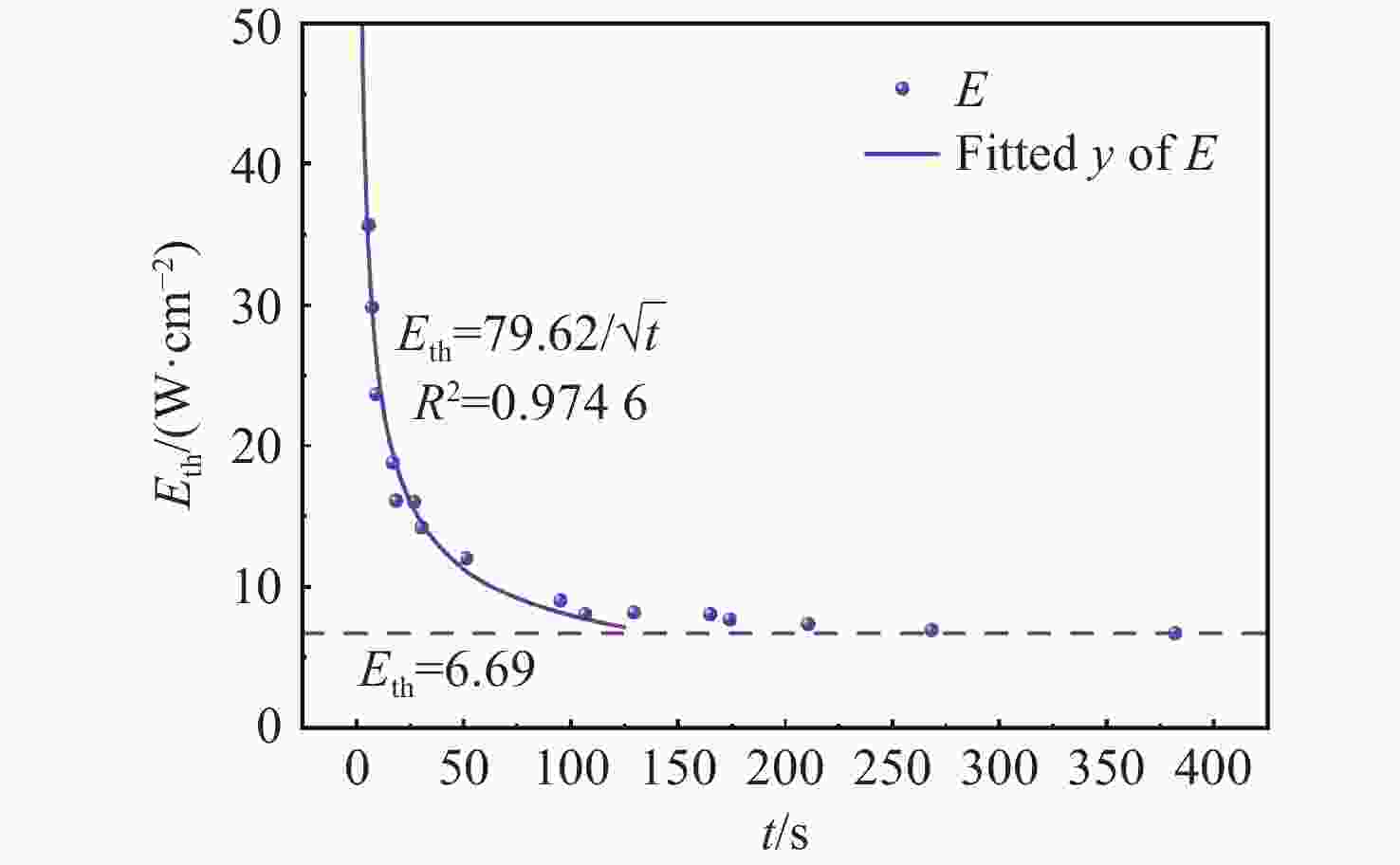
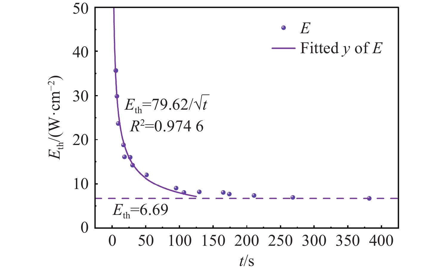
图 7 造成PIN管硬损伤的辐照度阈值(Eth)随辐照时间(t)的变化
Figure 7. Variation of power density threshold (Eth) for hard damage of the silicon PIN photodiodes with irradiation time (t)
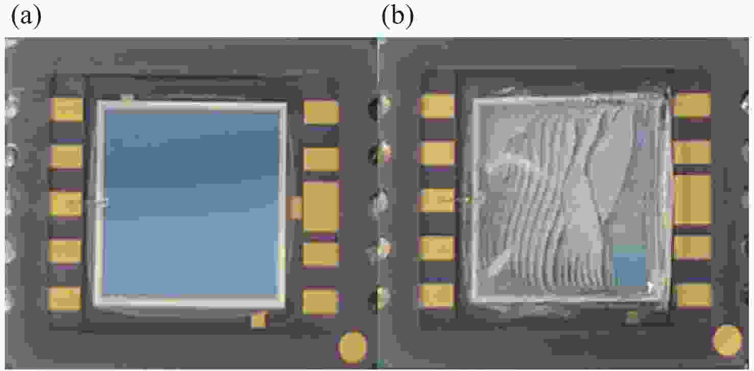
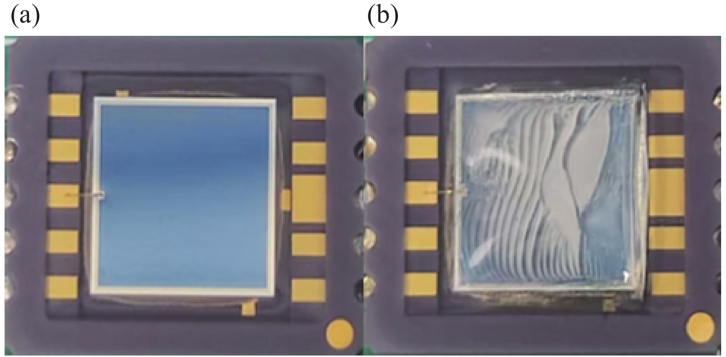
图 8 损伤前后PIN管的表面形貌差异。(a)损伤前PIN管表面形貌。(b)损伤后PIN管表面形貌,表面发生变化的区域为熔融开裂的硅橡胶
Figure 8. Surface morphology differences of the silicon PIN photodiodes before and after damage. (a) Surface morphology of the silicon PIN photodiode before damage. (b) Surface morphology of the silicon PIN photodiode after damage. The altered surface region is characterized by melting-induced cracking of the silicone rubber
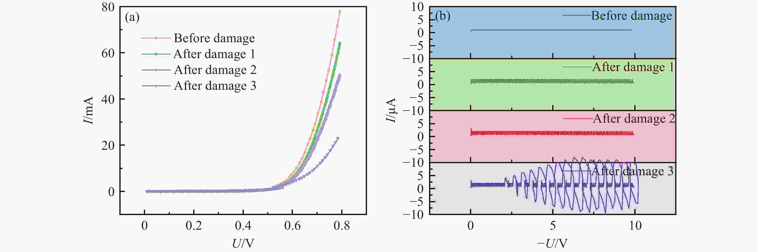
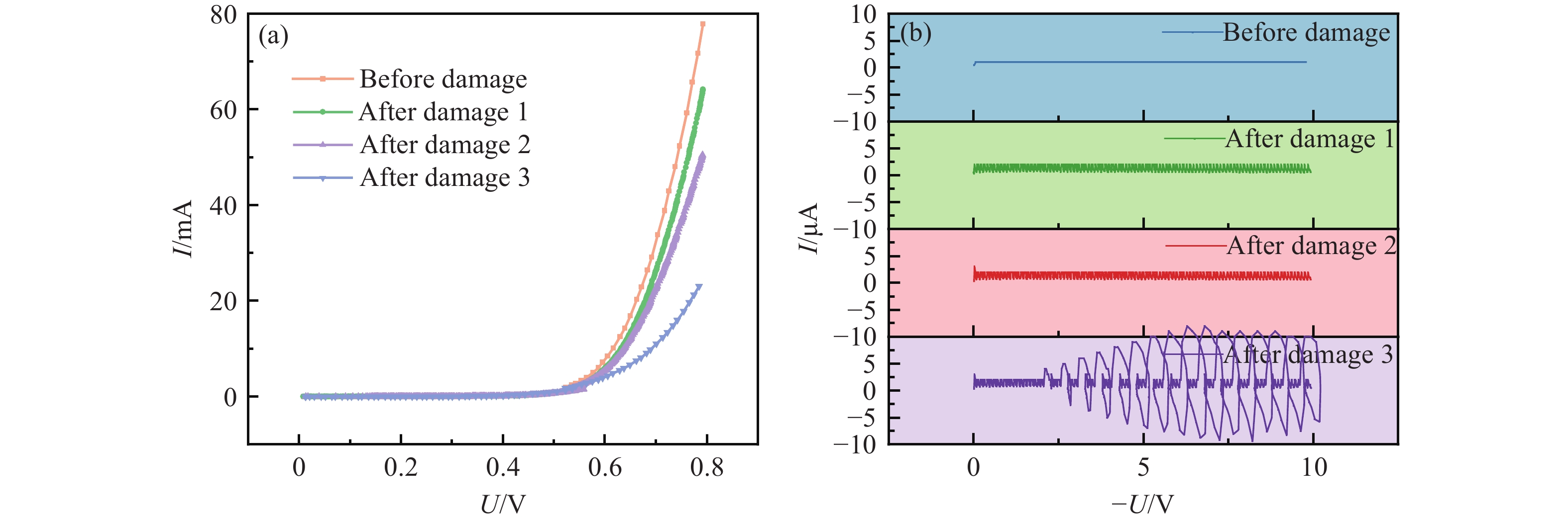
图 9 损伤前后PIN管电参数变化。(a)损伤前后PIN管的正向伏安特性曲线,橙色代表损伤前PIN管的正向伏安特性曲线,绿色、紫色、蓝色分别代表不同程度损伤后PIN管的伏安特性曲线。(b)损伤前后PIN管的漏电流(I)变化情况,图中纵坐标刻度范围一致,随着损伤程度增大,PIN管漏电流不稳定性增加
Figure 9. Variations in electrical parameters of the silicon PIN photodiode before and after damage. (a) Forward current-voltage (I-V) characteristics of the PIN photodiode before and after damage. The orange curve represents the forward I-V characteristic before damage; the green, purple, and blue curves represent the I-V characteristics after damage of increasing severity, respectively. (b) Variations in leakage current (I) before and after damage. The ordinate (vertical axis) scale is consistent across plots. Leakage current instability increases progressively with the extent of damage
表 1 PIN管探测能力的温度相关性拟合参数取值(R2>0.999)
Table 1. Fitting parameters for the temperature-dependent correlation of detectivity of silicon PIN photodiodes (R2>0.999)
E/(W·cm−2) 6.69 6.93 7.36 7.68 8.04 9.03 12.01 14.21 15.89 16.09 29.86 35.66 42.47 48.01 a −0.68 −0.35 −0.35 −0.68 −0.82 −0.80 −0.42 −0.43 −0.17 −0.17 −0.41 −0.28 −0.28 −0.27 b 1.77 1.47 1.46 1.79 1.93 1.89 1.51 1.51 1.25 1.23 1.50 1.35 1.40 1.35 c −0.002 −0.003 −0.003 −0.002 −0.002 −0.002 −0.003 −0.003 −0.004 −0.003 −0.003 −0.003 −0.003 −0.003  下载: 导出CSV
表 2 损伤前后PIN管漏电流变化情况
Table 2. Leakage current of the silicon PIN photodiodes before and after damage
S5106 Leakage current(VR=10 V) Before damage 0.30 µA After damage 1 0.36 µA After damage 2 0.40 µA After damage 3 0.42 µA
下载: 导出CSV
-
[1] SCHNEIDER-HORNSTEIN K, GOLL B, ZIMMERMANN H. Ultra-sensitive PIN-photodiode receiver[J]. IEEE Photonics Journal, 2023, 15(3): 7201409. doi: 10.1088/978-0-7503-5437-0ch6 [2] RA H S, LEE S H, JEONG S J, et al. Advances in heterostructures for optoelectronic devices: materials, properties, conduction mechanisms, device applications[J]. Small Methods, 2024, 8(2): 2300245. doi: 10.1002/smtd.202300245 [3] LI L L, ZHAO H T, LIU CH, et al. Intelligent metasurfaces: control, communication and computing[J]. eLight, 2022, 2(1): 7. doi: 10.1186/s43593-022-00013-3 [4] SUBLETTE C. Tumbler-snapper nuclear test series[EB/OL]. (2002-06-19)[2025-12-14]. https://nuclearweaponarchive.org/Usa/Tests/Tumblers.html. [5] ROCHA R, DE CASTRO J C V, DE CARVALHO SANTANA A. Evaluation of sun position and angular rates using the photovoltaic conversion system for on-board functions in an artificial satellite[J]. IEEE Transactions on Aerospace and Electronic Systems, 2024, 60(6): 9193-9203. doi: 10.1109/TAES.2024.3438088 [6] 王启明, 郭青, 孙若端, 等. 大动态范围阵列式光谱辐射计线性测量[J]. 光学学报, 2025, 45(11): 1112001. doi: 10.3788/AOS250707WANG Q M, GUO Q, SUN R D, et al. Linearity measurement of array spectroradiometer over large dynamic range[J]. Acta Optica Sinica, 2025, 45(11): 1112001. (in Chinese). doi: 10.3788/AOS250707 [7] GEIST J, ZALEWSKI E F, SCHAEFER A R. Spectral response self-calibration and interpolation of silicon photodiodes[J]. Applied Optics, 1980, 19(22): 3795-3799. doi: 10.1364/AO.19.003795 [8] NIE P, YU J Y, WEI ZH, et al. Investigation of silicon-based PIN photodetectors' surface damage features caused by continuous-nanosecond pulse combined laser[J]. Physics Letters A, 2025, 534: 130259. doi: 10.1016/j.physleta.2025.130259 [9] WEI Z, ZHANG W, WANG D, et al. Structural, optical and electrical behavior of millisecond pulse laser damaged silicon-based positive-intrinsic-negative photodiode[J]. Optik, 2017, 131: 110-115. doi: 10.1016/j.ijleo.2016.11.074 [10] MOROZOV A P, LUCHNIKOV L O, YURCHUK S Y, et al. Improvement of the perovskite photodiodes performance via advanced interface engineering with polymer dielectric[J]. Light: Advanced Manufacturing, 2025, 6(1): 24. [11] 王柯, 刘扬, 王云哲, 等. 纳秒脉冲激光对背照式CMOS探测器组件损伤机理研究[J]. 中国光学(中英文), 2025, 18(6): 1277-1288.WANG K, LIU Y, WANG Y ZH, et al. Investigation of laser-induced damage mechanisms in back-illuminated CMOS detector modules under nanosecond pulsed irradiation[J]. Chinese Optics, 2025, 18(6): 1277-1288. (in Chinese). [12] GAO L, WEI ZH, WANG D, et al. Experimental study of 1064nm CW laser ablation biased silicon-based PIN photodiodes[C]. Proceedings of SPIE 12060, AOPC 2021: Advanced Laser Technology and Applications, SPIE, 2021: 120601F. [13] LIANG H, ZHAO SH S, YU H J, et al. Study on HAZ extension characteristics during laser ablation of CFRP based on dimensional analysis[J]. Composites Part B: Engineering, 2024, 275: 111295. doi: 10.1016/j.compositesb.2024.111295 [14] 叶成, 邱荣, 蒋勇, 等. 1064nm和532nm纳秒激光同时辐照熔石英损伤规律的研究[J]. 强激光与粒子束, 2018, 30(4): 041003.YE CH, QIU R, JIANG Y, et al. Laser induced damage characteristics in fused silica surface irradiated by1064nm and 532nm ns laser simultaneously[J]. High Power Laser and Particle Beams, 2018, 30(4): 041003. (in Chinese). [15] LI S, HUANG L CH, YE J F, et al. Study on radiation damage of silicon solar cell electrical parameters by nanosecond pulse laser[J]. Electronics, 2024, 13(9): 1795. doi: 10.3390/electronics13091795 [16] WANG T T, LI P X, YU X Y, et al. High-energy hundred-picosecond fiber-solid hybrid laser and its application in laser-induced damage in PIN photodiode[J]. Laser Physics, 2020, 30(3): 036004. doi: 10.1088/1555-6611/ab6d65 [17] 王佳敏, 季艳慧, 梁志勇, 等. 532 nm皮秒脉冲激光对单晶硅的损伤特性研究[J]. 中国光学, 2022, 15(2): 242-250.WANG J M, JI Y H, LIANG ZH Y, et al. Damage characteristics of a 532 nm picosecond pulse laser on monocrystalline silicon[J]. Chinese Optics, 2022, 15(2): 242-250. (in Chinese). [18] KRUER M, ALLEN R, ESTEROWITZ L, et al. Laser damage in silicon photodiodes[J]. Optical and Quantum Electronics, 1976, 8(5): 453-458. doi: 10.1007/BF00624835 [19] KAFKA K R P, HOFFMAN B, HUANG H, et al. Pulse-length dependence of the laser-induced damage behavior of a fused-silica antireflective metasurface[J]. High Power Laser Science and Engineering, 2025, 13: e64. doi: 10.1017/hpl.2025.10036 [20] 罗福, 江继军, 孙承纬. 硅光电二极管激光损伤阈值随激光脉宽的变化[J]. 强激光与粒子束, 2004, 16(6): 685-688.LUO F, JIANG J J, SUN CH W. Variation in damage thresholds of Si photodiodes with laser pulse duration[J]. High Power Laser and Particle Beams, 2004, 16(6): 685-688. (in Chinese). [21] LOU W H, HU Y SH, JIA B N, et al. Laser-induced damage threshold based on thermal effects in high-purity silica optical fiber[J]. Optical Engineering, 2023, 62(7): 076102. doi: 10.1117/1.oe.62.7.076102 [22] CHANG H, ZHOU W J, MA Y J, et al. Damage characteristics of silicon solar cells induced by nanosecond pulsed laser[J]. Photonics, 2025, 12(8): 804. doi: 10.3390/photonics12080804 [23] LI Y R, CHEN J W, DUAN SH Y, et al. Thermal-mechanical-chemical coupled model and three-dimensional damage evaluation based on computed tomography for high-energy laser-ablated CFRP[J]. Composites Science and Technology, 2024, 258: 110867. doi: 10.1016/j.compscitech.2024.110867 [24] LIU K Y, ZHANG ZH W, TANG X Y, et al. Experimental and simulation study of single-event leakage current degradation and damage mechanism in 4H-SiC PiN diodes[J]. IEEE Transactions on Electron Devices, 2024, 71(8): 4891-4896. doi: 10.1109/TED.2024.3416421 [25] MIAO J J, ZHU CH Y, WULIJI H, et al. Study of convexity on nanosecond laser-induced damage growth in fused silica[J]. Optics & Laser Technology, 2025, 192: 113478. doi: 10.1016/j.optlastec.2025.113478 [26] BULGAKOV A V, SLÁDEK J, HRABOVSKÝ J, et al. Dual-wavelength femtosecond laser-induced single-shot damage and ablation of silicon[J]. Applied Surface Science, 2024, 643: 158626. doi: 10.1016/j.apsusc.2023.158626 [27] TIAN ZH Y, LOU J H, YANG L ZH, et al. Tunable high-flux solar simulator with enhanced uniformity for concentrated solar energy applications[J]. Applied Energy, 2024, 369: 123198. doi: 10.1016/j.apenergy.2024.123198 [28] WANG Y, SU SH, MENG F L, et al. Continuous irradiance adjustment system design for solar simulators with wide range and high uniformity[J]. Optical and Quantum Electronics, 2024, 56(5): 870. doi: 10.1007/s11082-023-06195-5 [29] MAO J H, WANG Y M, SHI E T, et al. Pre-launch multi-energy radiance calibration of the OMS-N[J]. Remote Sensing, 2023, 16(1): 119. doi: 10.3390/rs16010119 [30] 黎星宇. 基于光干扰条件下的大气层核爆光辐射信号识别方法研究[D]. 北京: 军事科学院, 2022.LI X Y. Research on recognition method of atmospheric nuclear explosion optical radiation under optical interference conditions[D]. Beijing: Academy of Military Sciences, 2022. (in Chinese). [31] REICH N H, VAN SARK W G J H M, ALSEMA E A, et al. Crystalline silicon cell performance at low light intensities[J]. Solar Energy Materials and Solar Cells, 2009, 93(9): 1471-1481. doi: 10.1016/j.solmat.2009.03.018 [32] HEIDRICH R, BARRETTA C, MORDVINKIN A, et al. UV lamp spectral effects on the aging behavior of encapsulants for photovoltaic modules[J]. Solar Energy Materials and Solar Cells, 2024, 266: 112674. doi: 10.1016/j.solmat.2023.112674 [33] KHAN F, SINGH S N, HUSAIN M. Effect of illumination intensity on cell parameters of a silicon solar cell[J]. Solar Energy Materials and Solar Cells, 2010, 94(9): 1473-1476. doi: 10.1016/j.solmat.2010.03.018 [34] 范永杰, 秦强. 激光辐照HgCdTe探测器输出特性与软损伤判定[J]. 红外技术, 2020, 42(9): 829-832.FAN Y J, QIN Q. HgCdTe detector output characteristics and soft damage determination under laser irradiation[J]. Infrared Technology, 2020, 42(9): 829-832. (in Chinese). [35] VEST R E, HILL S B, GRANTHAM S. Saturation effects in solid-state photodiodes and impact on EUVL pulse energy measurements[J]. Metrologia, 2006, 43(2): S84-S88. doi: 10.1088/0026-1394/43/2/S17 [36] SEEGER K. Miscellaneous semiconductors[M]//SEEGER K. Semiconductor Physics: An Introduction. 8th ed. Berlin, Heidelberg: Springer, 2002: 471-482. [37] 董先声, 施毅, 黎松林. 二维半导体的迁移率物理模型与仿真[J]. 中国科学: 信息科学, 2025, 55(12): 3080-3098. doi: 10.1360/SSI-2025-0417DONG X SH, SHI Y, LI S L. Physical models and simulation of carrier mobility in two-dimensional semiconductors[J]. Scientia Sinica: Informationis, 2025, 55(12): 3080-3098. (in Chinese). doi: 10.1360/SSI-2025-0417 [38] VAILLON R, PAROLA S, LAMNATOU C, et al. Solar cells operating under thermal stress[J]. Cell Reports Physical Science, 2020, 1(12): 100267. doi: 10.1016/j.xcrp.2020.100267 [39] ROY S, BARUAH M S, SAHU S, et al. Computational analysis on the thermal and mechanical properties of thin film solar cells[J]. Materials Today: Proceedings, 2021, 44(Pt 1): 1207-1213. [40] AL MAHDI H, LEAHY P G, ALGHOUL M, et al. A review of photovoltaic module failure and degradation mechanisms: causes and detection techniques[J]. Solar, 2024, 4(1): 43-82. doi: 10.3390/solar4010003 [41] SZE S M, NG K K. Physics and properties of semiconductors—a review[M]//SZE S M, NG K K. Physics of Semiconductor Devices. Hoboken: Wiley, 2006: 1. [42] KRISZTIÁN D, KORSÓS F, HAVASI G. Simultaneous measurement of charge carrier concentration, mobility, and lifetime[J]. Solar Energy Materials and Solar Cells, 2023, 260: 112461. doi: 10.1016/j.solmat.2023.112461 [43] COLWELL J, HSIAO P C, SHEN X W, et al. Impact of contact integrity during thermal stress testing on degradation analysis of copper-plated silicon solar cells[J]. Solar Energy Materials and Solar Cells, 2018, 174: 225-232. doi: 10.1016/j.solmat.2017.09.005 [44] WEI Y W, MA ZH, ZHAO X Y, et al. Improving the performance of Cu2ZnSn(S, Se)4 thin film solar cells by SCAPS simulation[J]. Materials Science and Engineering: B, 2024, 303: 117296. doi: 10.1016/j.mseb.2024.117296 [45] IBAÑEZ A, FATÁS E. Mechanical and structural properties of electrodeposited copper and their relation with the electrodeposition parameters[J]. Surface and Coatings Technology, 2005, 191(1): 7-16. [46] 顾晓春, 吴思汉. 微波pin二极管电阻与温度的关系[J]. 半导体技术, 2008, 33(12): 1066-1069,1073.GU X CH, WU S H. Relationship between resistance and temperature of microwave PIN diode[J]. Semiconductor Technology, 2008, 33(12): 1066-1069,1073. (in Chinese). [47] VAN NIJEN D A, NAOOM S, MUTTILLO M, et al. Analyzing the PN junction impedance of crystalline silicon solar cells across varied illumination and temperature conditions[J]. Solar Energy Materials and Solar Cells, 2025, 279: 113255. [48] RUSCHEL C S, GASPARIN F P, KRENZINGER A. Experimental analysis of the single diode model parameters dependence on irradiance and temperature[J]. Solar Energy, 2021, 217: 134-144. [49] CHEN P J, GE X, ZHANG ZH C, et al. Silicone-based thermally conductive gel fabrication via hybridization of low-melting-point alloy–hexagonal boron nitride–graphene oxide[J]. Nanomaterials, 2023, 13(3): 490. [50] CUCE E, CUCE P M, BALI T. An experimental analysis of illumination intensity and temperature dependency of photovoltaic cell parameters[J]. Applied Energy, 2013, 111: 374-382. [51] HUANG Y, YAN L, WU H, et al. New insights on generalized heat conduction and thermoelastic coupling models[J]. Applied Mathematics and Mechanics, 2025, 46(8): 1533-1550. [52] WU SH H, LIU J CH, ZHANG J Y, et al. Transient thermal response of quasi-continuous-wave laser diodes and its impact on saturation power[J]. Optics & Laser Technology, 2026, 193: 114269. [53] WEI ZH, YU J Y, GAO L, et al. Study of thermal effects in silicon-based PIN detectors with different external bias voltages irradiated by 1064 nm continuous laser[J]. Applied Physics B, 2024, 130(4): 58. [54] YIN J H, CUI Y W, SHANG Y Y, et al. Laser-induced damage thresholds prediction of functional ceramic films based on 3D thermal diffusion model[J]. Ceramics International, 2025, 51(7): 9100-9111. [55] LIU S Q, ZHENG ZH, MA Y, et al. Prediction of the damage threshold of CFRP irradiated by millisecond laser based on back propagation neural network[J]. Physica Scripta, 2025, 100(7): 076025. [56] KONG S, WANG R, FENG SH Y, et al. Tannic acid as a natural crosslinker for catalyst-free silicone elastomers from hydrogen bonding to covalent bonding[J]. Frontiers in chemistry, 2021, 9: 778896. [57] WEI ZH, YU J Y, ZUO M H, et al. Experimental study of millisecond pulse laser ablation biased silicon-based PIN photodiodes[J]. Journal of Applied Physics, 2024, 135(11): 115701. [58] 国家市场监督管理总局, 国家标准化管理委员会. GB/T 4587-2023 半导体器件 分立器件 第7部分: 双极型晶体管[S]. 北京: 中国标准出版社, 2023.State Administration for Market Regulation, National Standardization Administration. GB/T 4587-2023 Semiconductor devices - Discrete devices - Part 7: bipolar transistors[S]. Beijing: Standards Press of China, 2023. (in Chinese). [59] LIU H CH, PASANEN T P, FUNG T H, et al. Near-infrared germanium PIN-photodiodes with >1A/W responsivity[J]. Light: Science & Applications, 2025, 14(1): 9. [60] OMAR F A. Analysis of monocrystalline silicon solar cell performance under thermal stress, reverse bias stress, and AC impedance spectroscopy[J]. Discover Electronics, 2025, 2(1): 91. [61] FENG Y J, LI CH, LIU Q L, et al. Scalability of dark current in silicon PIN photodiode[J]. Chinese Physics B, 2018, 27(4): 048501. [62] MOEGLIN J P, GAUTIER B, JOECKLÉ R, et al. Electrical behaviour of laser-damaged silicon photodiodes[J]. Optics and Lasers in Engineering, 1997, 28(5): 317-330. [63] ENCINAS-SANZ F, GUERRA J M. Laser-induced hot carrier photovoltaic effects in semiconductor junctions[J]. Progress in Quantum Electronics, 2003, 27(4): 267-294. [64] TANG H B, LIN H, WANG G SH, et al. Understanding localized current leakage in silicon-based heterojunction solar cells[J]. Progress in Photovoltaics: Research and Applications, 2025, 33(4): 522-530. -

 下载:
下载:


计量
- 文章访问数: 225
- HTML全文浏览量: 110
- PDF下载量: 34
- 被引次数: 0
