


Research on optical path optimization design and signal enhancement technology for direct optical film thickness control systems
-
摘要:
随着光电技术的发展,光学薄膜广泛应用于军事、医疗、通信等领域,膜层厚度是决定其光学性能的关键参数,膜厚监控系统的精度直接影响光谱性能。针对直控式光学膜厚监控系统光源发散、探测器响应信号弱的波段引起厚度控制误差大的问题,本文提出将光信号发射与接收端均放置在真空腔外,避免腔室的振动、温度、装配等对光信号的干扰,基于光纤耦合与准直聚焦的光信号调制方案,通过将光源外置并集成化设计,结合多模光纤与复合光路系统,利用Zemax软件以监控镜片和光纤接收端面的光斑尺寸及能量密度为目标,优化光信号发射和接收端光学系统元件的参数,提高光信号及电信号的稳定性。改进后光纤接收端辐照强度提升222.7%,信号强度提升156.6%,信噪比提高70.38%。通过制备波长
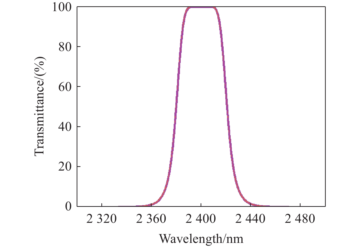
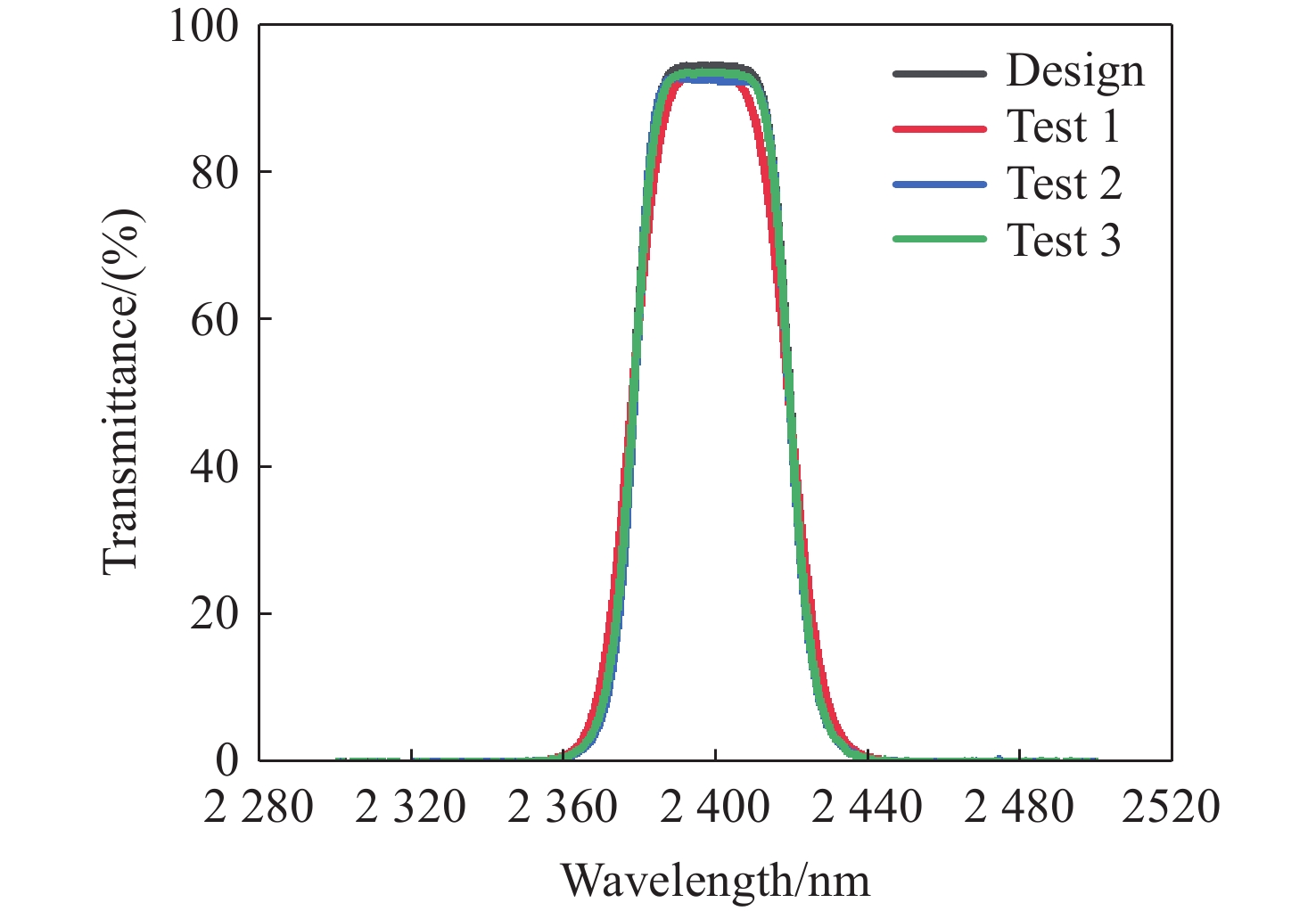
2400 nm、半高宽40 nm的窄带滤光膜,重复制备三次中心波长偏移在1 nm以内,半带宽均为40 nm。从而验证该系统在探测器响应信号弱的波段实现高精度、高稳定性膜厚监控。Abstract:With the advancement of photoelectric technology, optical films are extensively employed in military, medical, and communication fields. Film thickness is a critical parameter that determines optical performance, and the accuracy of its monitoring system directly affects spectral characteristics. To mitigate the significant thickness control errors in conventional direct monitoring systems—caused by light source divergence and weak detector response signals—this paper proposes an externalized optical configuration. In this design, both the optical transmitter and receiver are placed outside the vacuum chamber, thereby avoiding interference from chamber vibration, temperature variations, and assembly inconsistencies. Additionally, an optical signal modulation scheme based on fiber coupling and collimation-focusing is introduced. By adopting an external integrated light source combined with multimode optical fibers and a composite optical path, and by optimizing component parameters through optical simulation to improve spot quality and energy density, the stability of both optical and electrical signals is enhanced. After optimization, irradiance at the fiber receiving end increased by 222.7%, signal strength by 156.6%, and the signal-to-noise ratio by 70.38%. The system’s performance was validated by preparing a narrowband filter film with a center wavelength of
2400 nm and a bandwidth of 40 nm, achieving a wavelength deviation within 1 nm over three repeated tests while consistently maintaining the 40 nm bandwidth. These results confirm that the system enables high-precision and stable film thickness monitoring even in spectral bands with weak detector response. -
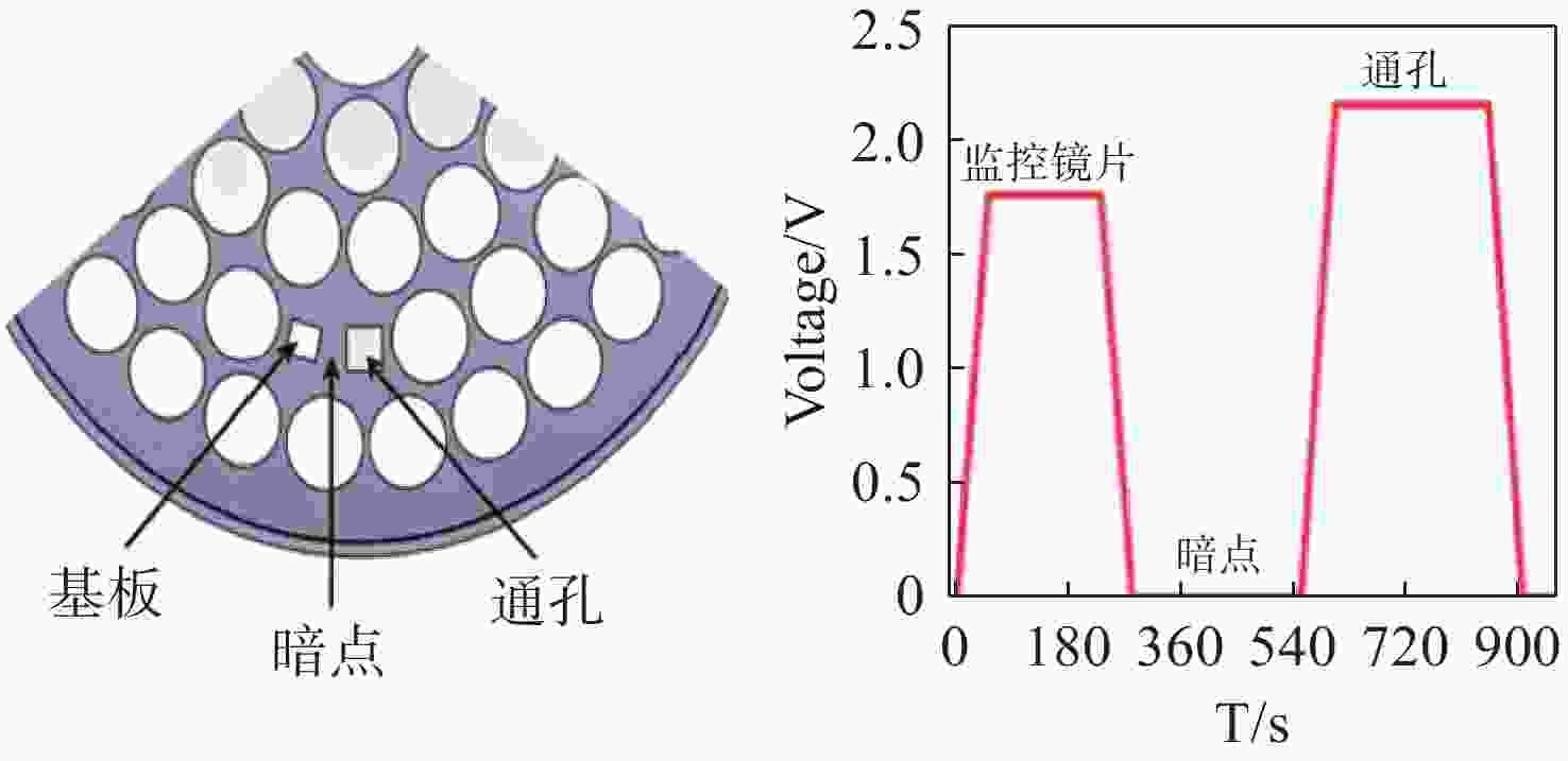
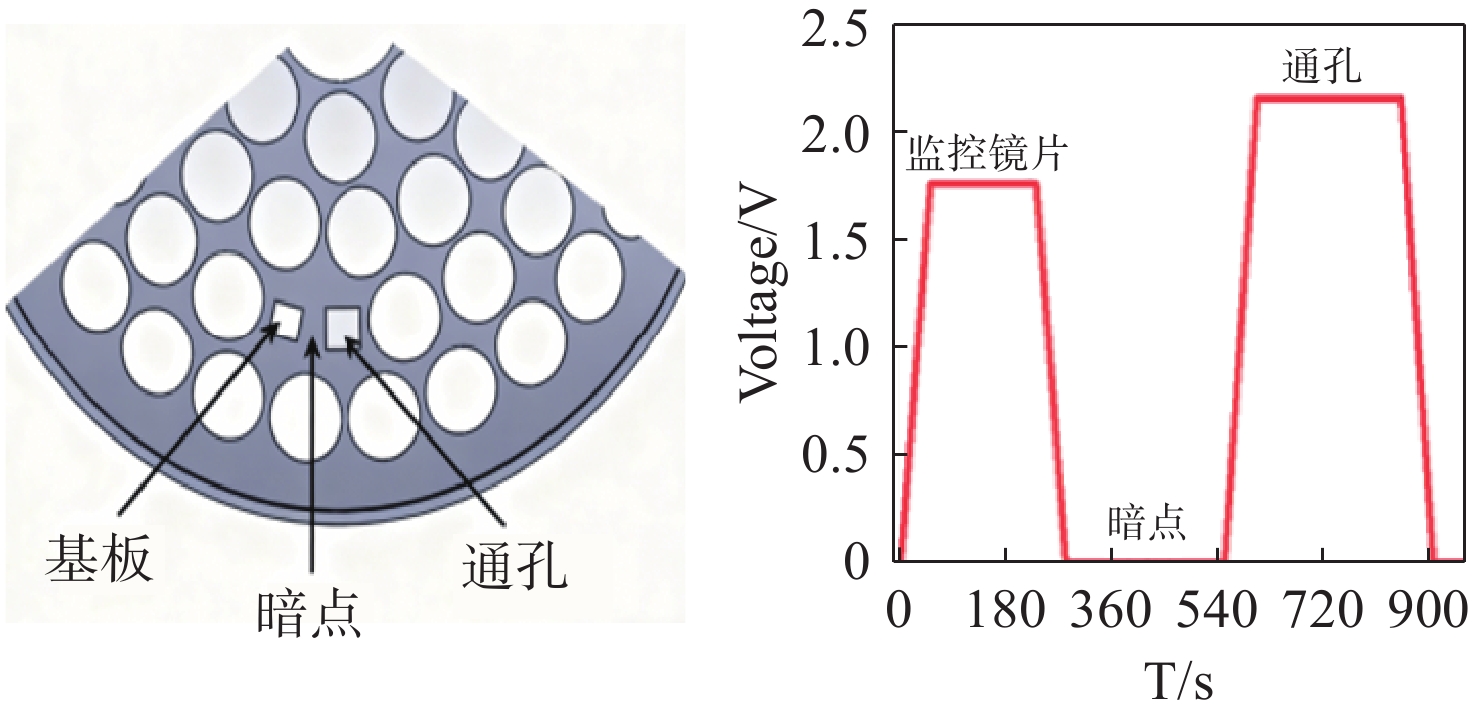
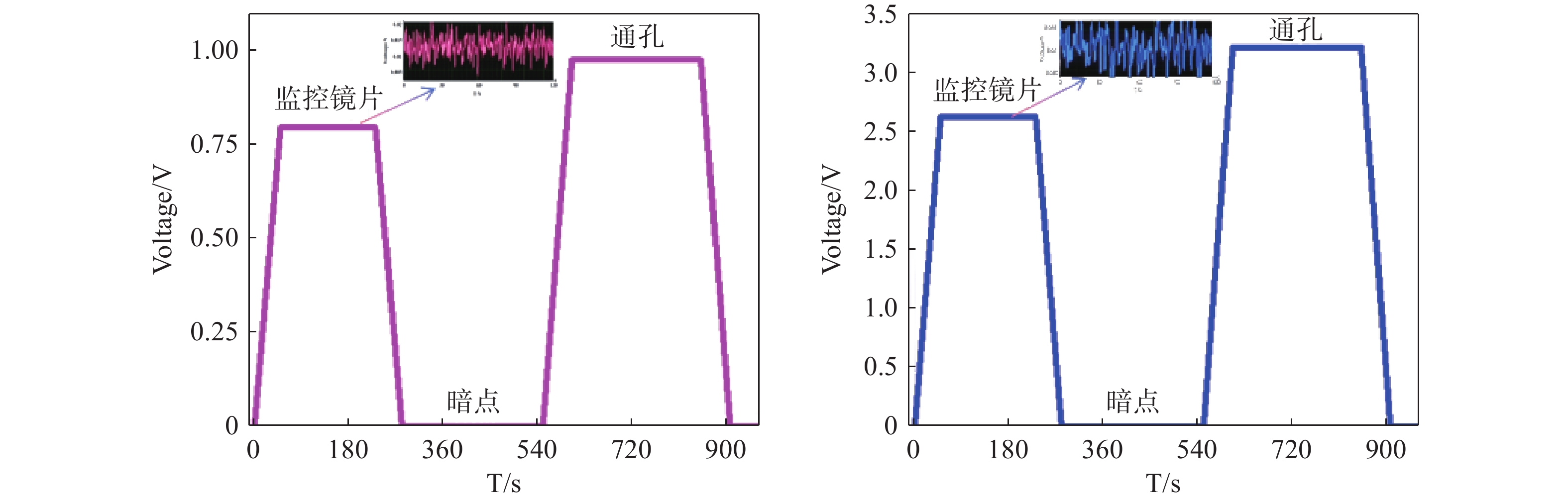
图 2 工件盘开孔及调制信号采样示意图
Figure 2. Schematic of the Substrate Holder Aperture and Modulated Signal Sampling
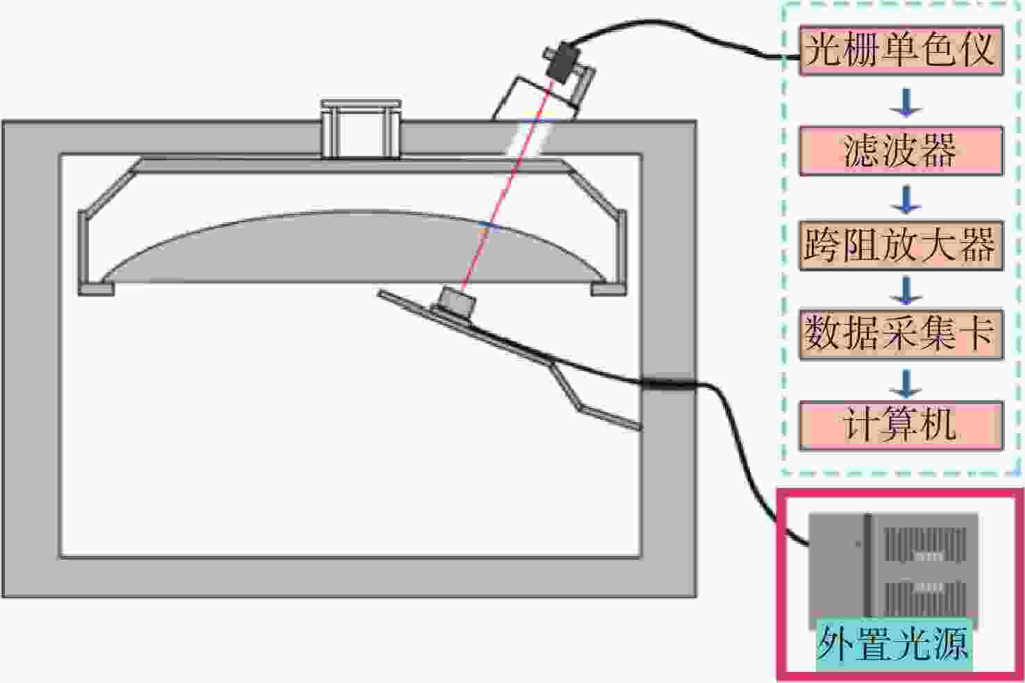
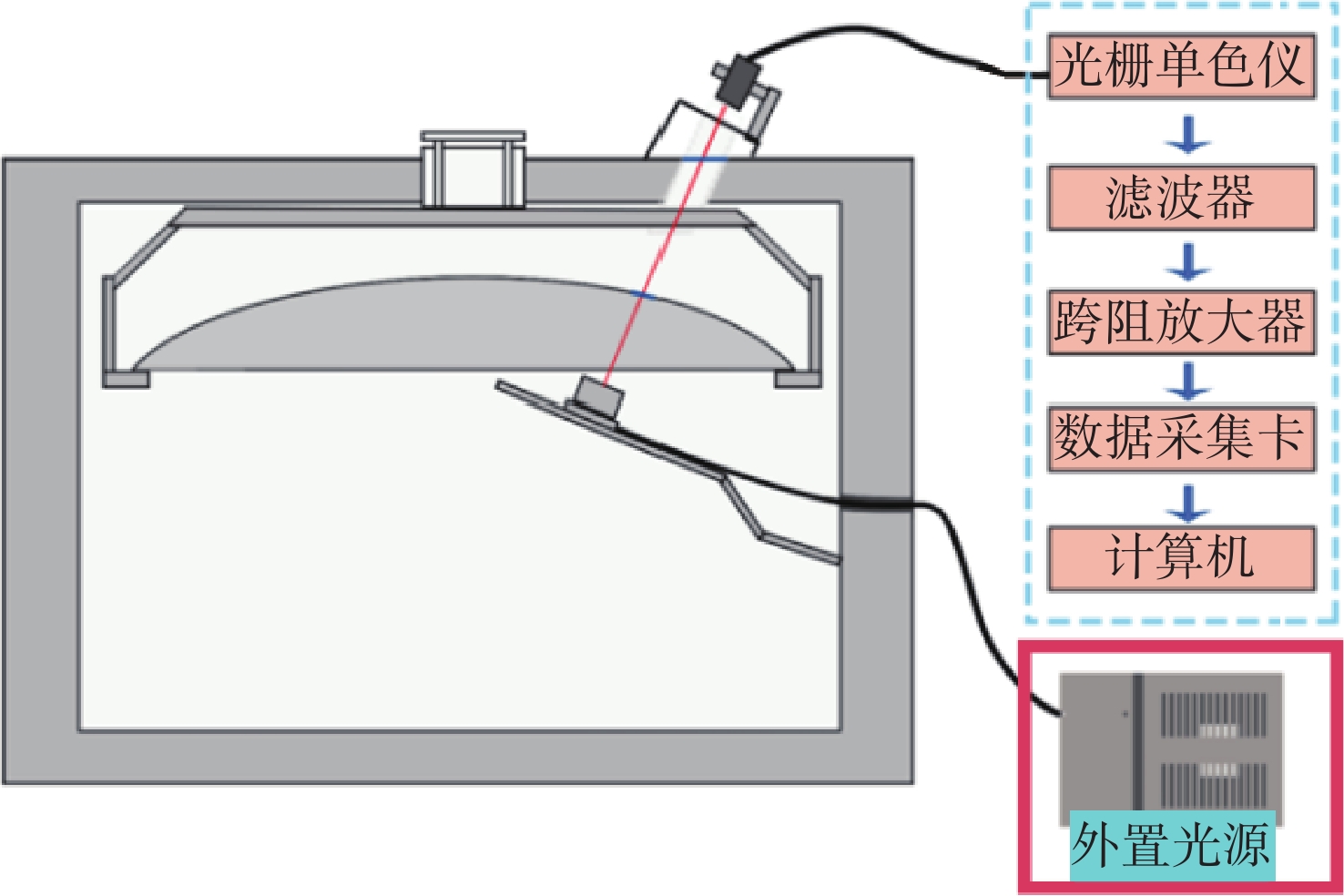
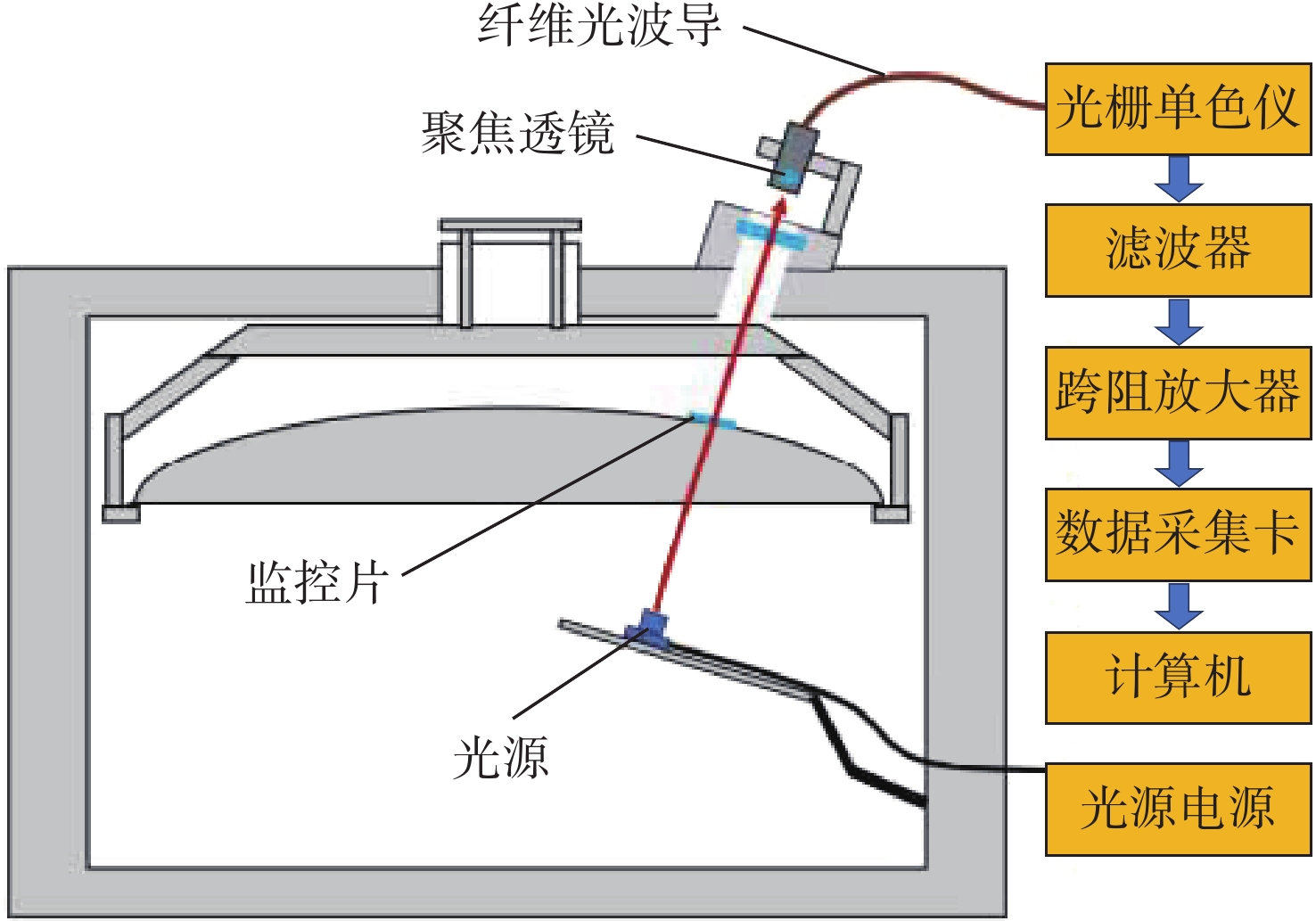
图 3 新直控式光学膜厚监控系统结构简图
Figure 3. Structural Schematic of the Proposed Direct-Monitoring Optical Film Thickness System
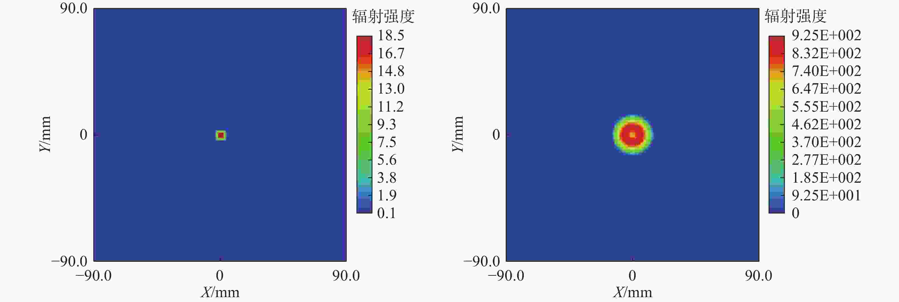
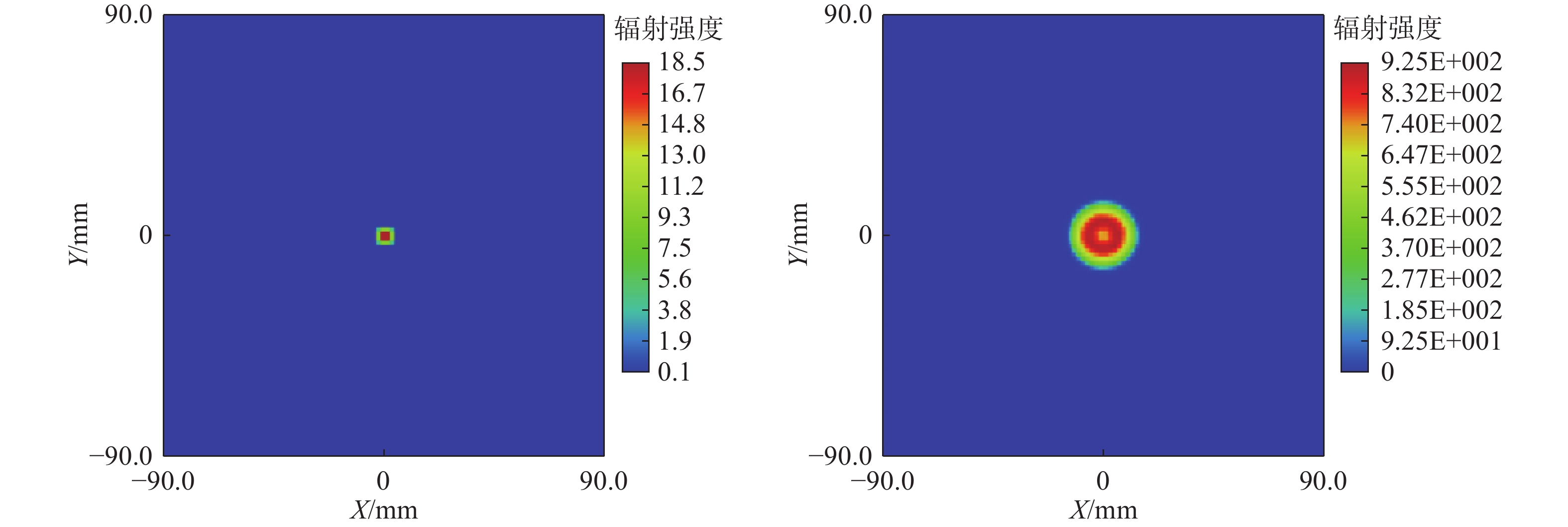
图 6 优化前(左)、优化后(右)光纤入射端辐射强度
Figure 6. Radiance at the Fiber Input End Before (Left) and After (Right) Optimization
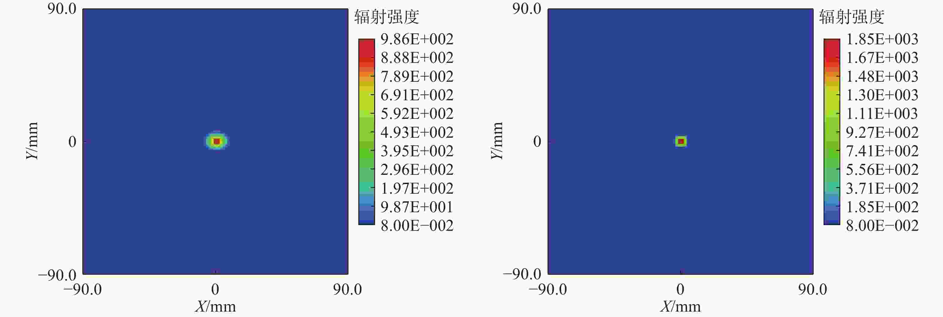
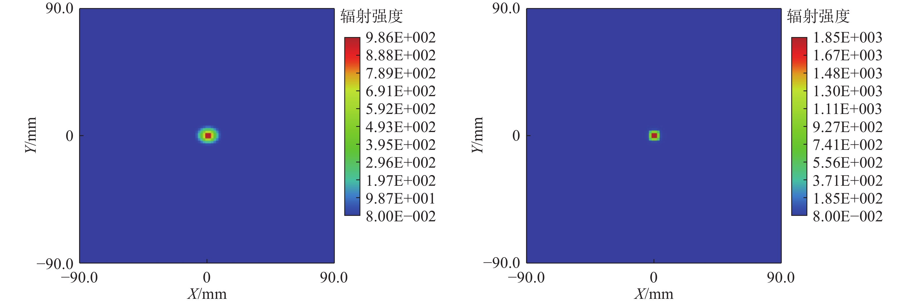
图 7 优化前(左)、优化后(右)监控镜片接收辐射强度
Figure 7. Radiance at the Receiving End of the Monitoring Lens Before (Left) and After (Right) Optimization
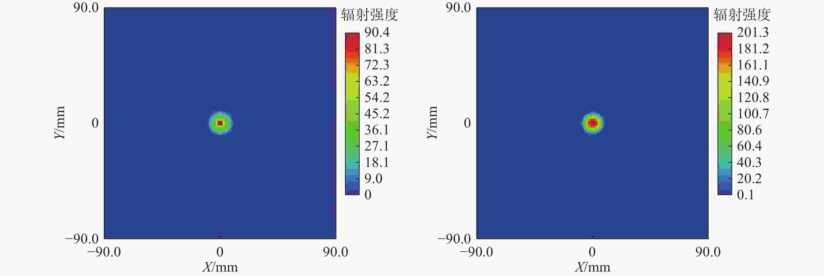
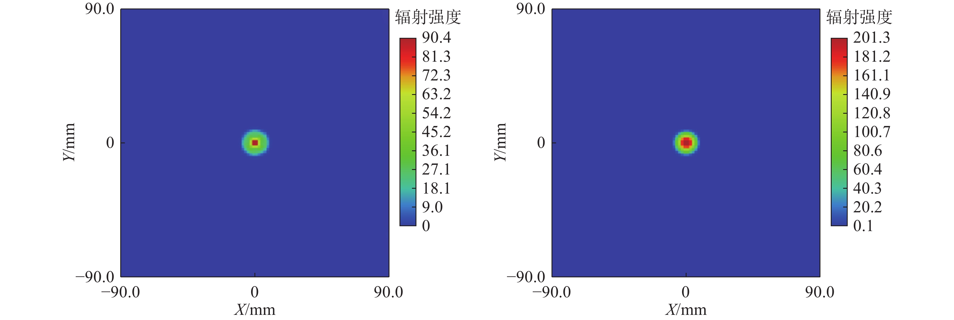
图 8 增加会聚透镜前(左)、后(右)光纤出射端接收辐照强度
Figure 8. Irradiance at the Fiber Output End Before (Left) and After (Right) Adding the Converging Lens
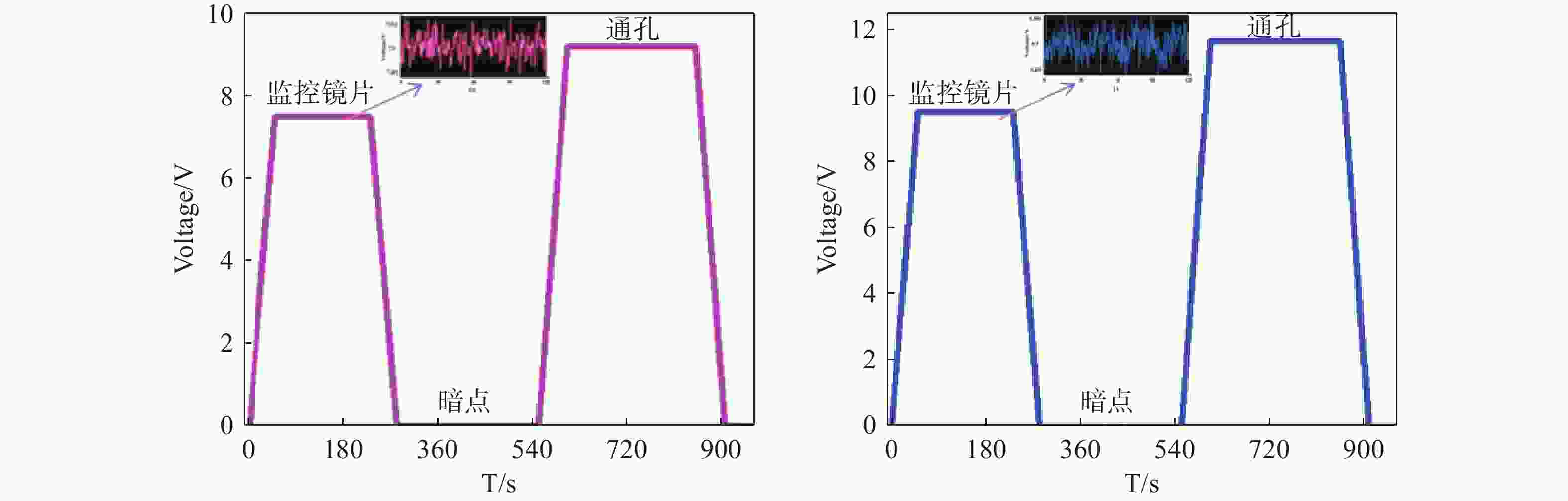
图 11
2400 nm优化前后信号幅值Figure 11. Signal Amplitude at
2400 nm: Pre- vs Post-Optimization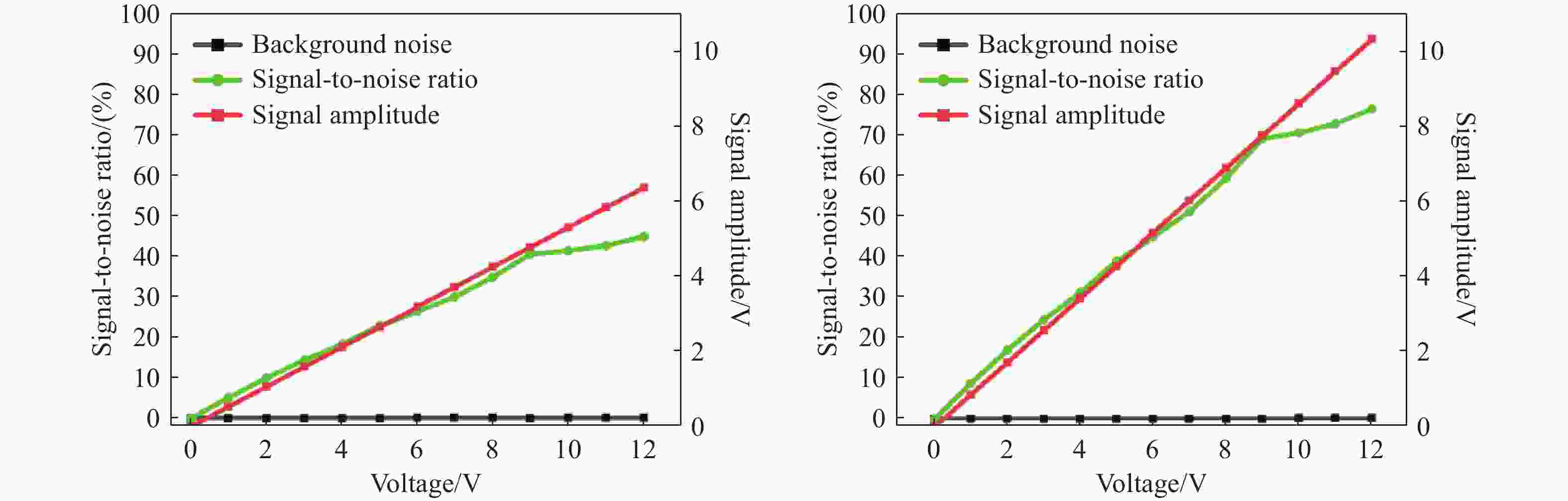
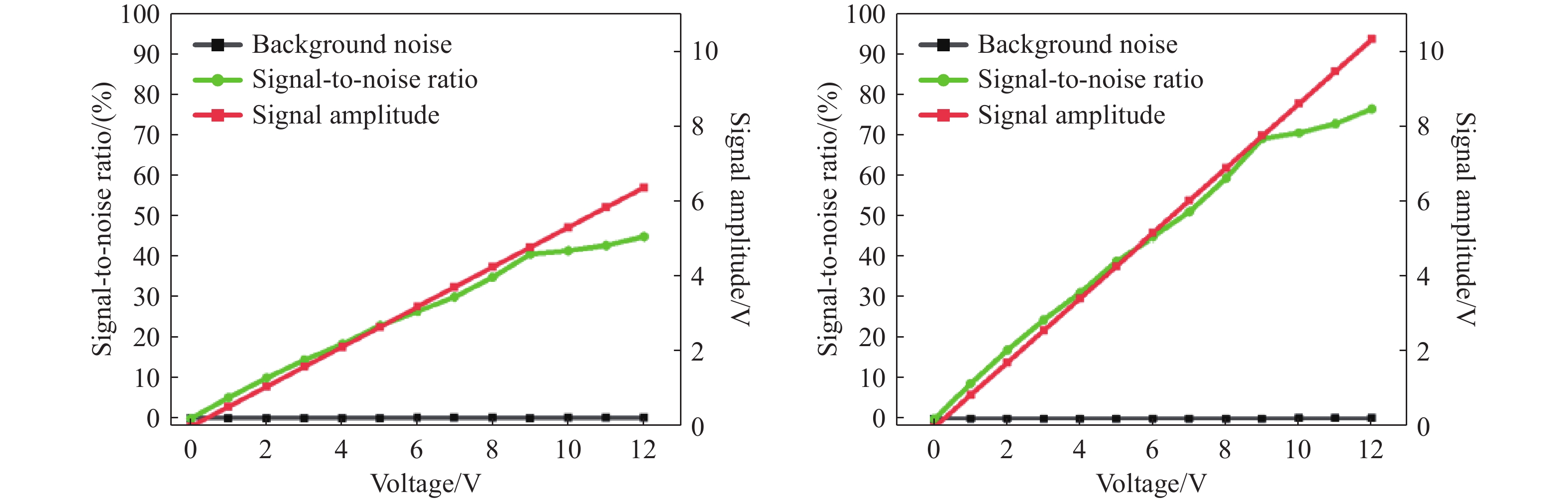
图 12 底噪、信噪比与信号幅值关系曲线
Figure 12. Relationship Between Noise Floor, SNR, and Signal Amplitude
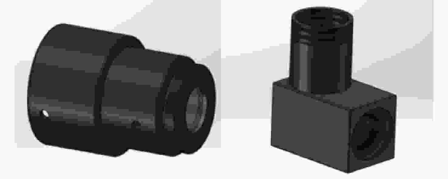
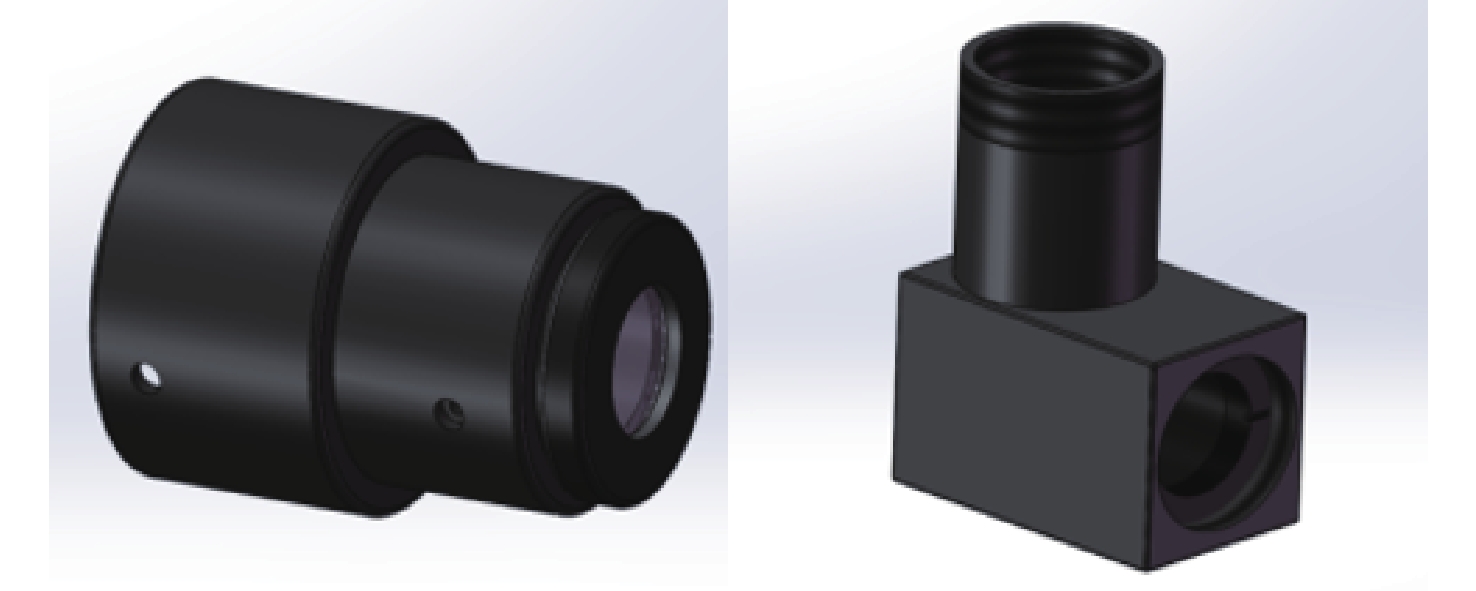
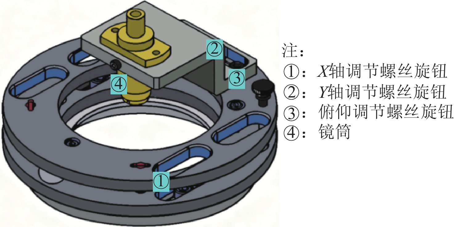
图 13 光源端镜筒(左)、真空室内镜筒(右)
Figure 13. Lens tube at the light source end (left), lens tube in the vacuum chamber (right)
表 1 光路系统优化关键指标
Table 1. Key Indicators for Optical Path System Optimization
系统参数 数值 光纤出射端-监控镜片距离/mm 20≤L≤40 光纤数值孔径角 0.22 光纤接收端光斑直径/mm 1.2 光强均匀性 RSD≤10% 透镜中心厚度/mm ≥0.8  下载: 导出CSV
表 2 阶跃型多模光纤参数
Table 2. Parameters of Multimode Optical Fibers
参数 名称/数值 芯层材料 纯石英 包层材料 F掺杂石英 芯层直径/μm 200±5.0 包层直径/μm 220±6.0 折射率结构 阶跃型 数值孔径/NA 0.22±0.02 工作波长范围/nm 400− 2400
下载: 导出CSV
表 3 优化后准直聚焦系统参数
Table 3. Parameters of the optimized collimation and focusing system
准直透镜 会聚透镜 材质 BK7 F9 直径/mm 30 28 曲率半径/mm r1=55,r2=40 r1=r2=50 中心厚度/mm 4.2 3.6 焦距/mm 76 58
下载: 导出CSV
表 4 腔室内部光学系统参数
Table 4. Initial structural Parameters of the lens
反射镜 会聚透镜 材质 紫外熔石英 紫外熔石英 直径/mm 25 31 曲率半径/mm 平面 r1=r2=65 中心厚度/mm 4 4 焦距/mm / 72
下载: 导出CSV
表 5 接收端会聚的双凸透镜参数
Table 5. Parameters of the converging lens at the receiving end
材质 直径/mm 曲率半径/mm 中心厚度/mm 焦距/mm BK7 30 r1=r2=60 4 65
下载: 导出CSV
表 6 装配误差分析
Table 6. Assembly Error Analysis
装配对象 公差 辐照强度变化/% 光源端
透镜组Z轴偏差:+1 mm 2.57 Z轴偏差:−1 mm 2.65 Y轴偏差:+1 mm 2.71 Y轴偏差:−1 mm 2.66 X轴偏差:+1 mm 1.96 X轴偏差:−1 mm 2.10 真空室内
透镜组Z轴偏差:+1 mm 2.35 Z轴偏差:−1 mm 2.46 Y轴偏差:+1 mm 2.51 Y轴偏差:−1 mm 2.49 X轴偏差:+1 mm 2.55 X轴偏差:−1 mm 2.52 光纤
接收端面Z轴偏差:+1 mm 23.70 Z轴偏差:−1 mm 24.03 Y轴偏差:+1 mm 15.17 Y轴偏差:−1 mm 15.36 X轴偏差:+1 mm 17.66 X轴偏差:−1 mm 17.62
下载: 导出CSV
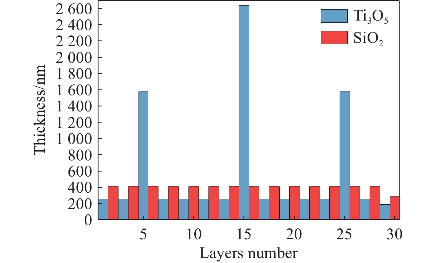
表 7 工艺参数
Table 7. Process Parameters of Ion Source
材料 蒸发
速率
/ Å/S充
氧
量离子源参数 电压/V 电流/mA 流速/SCCM 离子源清洗 750 750 8(Ar),50(O2) Ti3O5 0.4 30 1150 950 8(Ar),50(O2) SiO2 0.6 0 1150 950 8(Ar),50(O2)
下载: 导出CSV
-
[1] 唐晋发, 顾培夫, 刘旭. 现代光学薄膜技术[M]. 杭州: 浙江大学出版社, 2006.TANG J F, GU P F, LIU X. Modern Optical Thin Film Technology[M]. Hangzhou: Zhejiang University Press, 2006. (in Chinese). [2] 庄秋慧, 王三强. 光学膜厚的监控方法[J]. 激光与光电子学进展, 2018, 55(10): 103102. doi: 10.3788/LOP55.103102ZHUANG Q H, WANG S Q. Monitoring method of optical film thickness[J]. Laser & Optoelectronics Progress, 2018, 55(10): 103102. (in Chinese). doi: 10.3788/LOP55.103102 [3] 常敏, 华博, 张学典, 等. 光电极值法结合外差干涉法监控膜厚的研究[J]. 光学技术, 2017, 43(2): 184-186. doi: 10.13741/j.cnki.11-1879/o4.2017.02.020CHANG M, HUA B, ZHANG X D, et al. Study on film monitoring based on the photoelectric extreme value method combined with heterodyne interferometry[J]. Optical Technique, 2017, 43(2): 184-186. (in Chinese). doi: 10.13741/j.cnki.11-1879/o4.2017.02.020 [4] BRUNS S, FARR P, MELZIG T, et al. Improving optical thickness monitoring by including systematic and process-influenced transmittance deviations[J]. Applied Optics, 2023, 62(7): B141-B147. doi: 10.1364/AO.475076 [5] LI N, WANG G H, BAI X S, et al. Effect of quartz crystal thermal stress on its performance in active temperature control quartz crystal microbalance dew point sensors[J]. Sensors and Actuators B: Chemical, 2022, 369: 132283. doi: 10.1016/j.snb.2022.132283 [6] DONG S T, FU X H, LI CH. Noble infrared optical thickness monitoring system based on the algorithm of phase-locked output current–reflectivity coefficient[J]. Coatings, 2022, 12(6): 782. doi: 10.3390/coatings12060782 [7] MELZIG T, AMOCHKINA T, BRUNS S, et al. Influence of fitting algorithms on thickness determination during monitoring of optical coatings[J]. Surface and Coatings Technology, 2024, 476: 130197. doi: 10.1016/j.surfcoat.2023.130197 [8] 杜昕, 付秀华, 董所涛, 等. 变量耦合动态监控光学膜厚补偿技术[J]. 中国光学(中英文), 2025, 18(3): 467-476.DU X, FU X H, DONG S T, et al. Variable coupling dynamic monitoring and compensation technology of optical film thickness[J]. Chinese Optics, 2025, 18(3): 467-476. (in Chinese). [9] MELZIG T, AMOCHKINA T, BRUNS S, et al. Influence of fitting algorithms on thickness determination during monitoring of optical coatings[J]. Surface and Coatings Technology, 2024, 476: 130197. (查阅网上资料, 本条文献与第7条文献重复, 请确认). [10] 谢海峰, 付秀华, 董所涛, 等. 膜厚监控系统准直聚焦耦合光路的研制[J]. 光学 精密工程, 2025, 33(1): 25-36.XIE H F, FU X H, DONG S T, et al. Development of collimated focus coupled optical path for film thickness monitoring system[J]. Optics and Precision Engineering, 2025, 33(1): 25-36. (in Chinese). [11] BRUNS S, FARR P, MELZIG T, et al. Improving optical thickness monitoring by including systematic and process-influenced transmittance deviations[J]. Applied Optics, 2023, 62(7): B141-B147. (查阅网上资料, 本条文献与第4条文献重复, 请确认). [12] TIKHONRAVOV A, KOCHIKOV I, SHARAPOVA S, et al. Optical monitoring of coating production: correlation of errors and errors self-compensation[J]. Proceedings of SPIE, 2021, 11872: 118720Q. [13] 杨琪, 曾敏, 周文祺, 等. 基于直流磁控溅射VO2薄膜的高效近红外光电探测器[J]. 发光学报, 2025, 46(11): 2119-2128. doi: 10.37188/CJL.20250148YANG Q, ZENG M, ZHOU W Q, et al. DC magnetron-sputtered VO2 thin films: towards high-performance near-infrared photodetectors[J]. Chinese Journal of Luminescence, 2025, 46(11): 2119-2128. (in Chinese). doi: 10.37188/CJL.20250148 [14] 张丹丹, 黄芷婷, 李君, 等. 半导体激光器与光纤耦合效率仿真分析[J/OL]. 应用光学, 2025: 1-15 (2025-09-01)[2025-11-24]. https://link.cnki.net/urlid/61.1171.O4.20250901.1415.002.ZHANG D D, HUANG ZH T, LI J, et al. Optimization of coupling efficiency between semiconductor laser and fiber based on intelligent algorithm[J/OL]. Journal of Applied Optics, 2025: 1-15 (2025-09-01)[2025-11-24]. https://link.cnki.net/urlid/61.1171.O4.20250901.1415.002. (in Chinese). [15] 王锦荣, 叶建春, 侯丽英, 等. 基于Zemax非球面单透镜的优化设计[J]. 空间电子技术, 2024, 21(5): 87-92. doi: 10.3969/j.issn.1674-7135.2024.05.013WANG J R, YE J CH, HOU L Y, et al. The optimum design of aspherical single lens based on Zemax[J]. Space Electronic Technology, 2024, 21(5): 87-92. (in Chinese). doi: 10.3969/j.issn.1674-7135.2024.05.013 [16] 周双, 刘子建. 光学系统装配误差分析及装调路径优选[J]. 机械设计与制造, 2022, 371(1): 159-163,167. doi: 10.3969/j.issn.1001-3997.2022.01.036ZHOU SH, LIU Z J. The assembly error analysis of optical system and path optimization of alignment[J]. Machinery Design & Manufacture, 2022, 371(1): 159-163,167. (in Chinese). doi: 10.3969/j.issn.1001-3997.2022.01.036 -

 下载:
下载:

计量
- 文章访问数: 160
- HTML全文浏览量: 92
- PDF下载量: 4
- 被引次数: 0
