| Citation: | GAO Feng, QIN Li, CHEN Yong-yi, JIA Peng, CHEN Chao, LIANG Lei, CHEN Hong, ZHANG Xing, NING Yong-qiang. Reseach progress of bent waveguide and its applications[J]. Chinese Optics, 2017, 10(2): 176-193. doi: 10.3788/CO.20171002.0176

|

| [1] |
CHEN R, NG K W, KO W S, et al.. Nanophotonic integrated circuits from nanoresonators grown on silicon[J]. Nature Communications, 2014, 5:1-9. https://www.researchgate.net/publication/263708999_Nanophotonic_integrated_circuits_from_nanoresonators_grown_on_silicon
|
| [2] |
DAI D, WU H, GUAN X. SOI (Silicon-on-insulator)-compatible hybrid nanoplasmonics:waveguiding, polarization-handling, and thermal-tuning[J]. Nanophotonics and Micro/Nano Optics Ⅱ, 2014:9277.
|
| [3] |
DAI D X, BAUTERS J, BOWERS J E. Passive technologies for future large-scale photonic integrated circuits on silicon:polarization handling, light non-reciprocity and loss reduction[J]. Light-Sci. Appl., 2012, 1:12. doi: 10.1038/lsa.2012.12
|
| [4] |
BOEUF F, CREMER S, VULLIET N, et al.. A multi-wavelength 3D-compatible silicon photonics platform on 300 mm SOI wafers for 25 Gb/s applications[C]. IEDM, 2013:13.13.11-13.13.14.
|
| [5] |
WELCH DF, KISH FA, MELLE S, et al.. Large-Scale InP photonic integrated circuits:enabling efficient scaling of optical transport networks[J]. IEEE J. Selected Topics in Quantum Electronics, 2007, 13(1):22-31. doi: 10.1109/JSTQE.2006.890068
|
| [6] |
NICHOLES S C, MASANOVIC M L, JEVREMOVIC B, et al.. An 88 InP Monolithic Tunable Optical Router (MOTOR) packet forwarding chip[J]. J. Lightwave Technology, 2010, 28(4):641-650. doi: 10.1109/JLT.2009.2030145
|
| [7] |
TAYLOR H F. Power loss at directional change in dielectric waveguides[J]. Applied Optics, 1974, 13(3):642-647. doi: 10.1364/AO.13.000642
|
| [8] |
LADOUCEUR F, LABEYE P. A new general-approach to optical wave-guide path design[J]. J. Lightwave Technology, 1995, 13(3):481-492. doi: 10.1109/50.372446
|
| [9] |
SUBBARAMAN H, XU X, HOSSEINI A, et al.. Recent advances in silicon-based passive and active optical interconnects[J]. Optics Express, 2015, 23(3):2487-2510. doi: 10.1364/OE.23.002487
|
| [10] |
SMIT M K. InP photonic integrated circuits[J]. IEEE J. Selected Topics in Quantum Electronics, 2002, 16(5):1113-1125.
|
| [11] |
KAWACHI M. Recent progress in silica-based planar lightwave circuits on silicon[J]. Optoelectronics, IEE Proceedings, 1996, 143(5):257-262. doi: 10.1049/ip-opt:19960493
|
| [12] |
ZHANG X, HOSSEINI A, LIN X, et al.. Polymer-based hybrid integrated photonic devices for silicon on-chip modulation and board-level optical interconnects[J]. IEEE J. Selected Topics in Quantum Electronics, 2014, 19(6):3401115. http://www.oalib.com/paper/3579041
|
| [13] |
LEE H, CHEN T, LI J, et al.. Ultra-low-loss optical delay line on a silicon chip[J]. Nature Communications, 2012, 3:7.
|
| [14] |
BAUTERS J F, HECK M J R, JOHN D, et al.. Ultra-low-loss high-aspect-ratio Si3N4 waveguides[J]. Optics Express, 2011, 19(4):3163-3174. doi: 10.1364/OE.19.003163
|
| [15] |
BAUTERS J F, HECK M J, JOHN D D, et al. Planar waveguides with less than 0.1 dB/m propagation loss fabricated with wafer bonding[J]. Optics Express, 2011, 19(24):24090-24101. doi: 10.1364/OE.19.024090
|
| [16] |
ADAR R, SERBIN M R, MIZRAHI V. Less than 1 dB per meter propagation loss of silica wave-guides measured using a ring resonator[J]. J. Lightwave Technology, 1994, 12(8):1369-1372. doi: 10.1109/50.317523
|
| [17] |
KOBAYASHI N, SATO K, NAMIWAKA M, et al.. Silicon photonic hybrid ring-filter external cavity wavelength tunable lasers[J]. J. Lightwave Technology, 2015, 33(6):1241-1246. doi: 10.1109/JLT.2014.2385106
|
| [18] |
SOREF R A, LARENZO J. All-silicon active and passive guided-wave components for λ=1.3 and 1.6μm[J]. IEEE J. Quantum Electronics, 1986, 22(6):873-879. doi: 10.1109/JQE.1986.1073057
|
| [19] |
SOREF R A. Silicon-based optoelectronics[J]. Proceedings of the IEEE, 1994, 23(12):1687-1706.
|
| [20] |
JALALI B, TRINH P D, YEGNANARAYANAN S, et al.. Guided-wave optics in silicon-on-insulator technology[J]. IEE Proceedings-optoelectronics, 1996, 143(5):307-311. doi: 10.1049/ip-opt:19960675
|
| [21] |
JALALI B, YEGNANARAYANAN S, YOON T, et al.. Advances in silicon-on-insulator optoelectronics[J]. IEEE J. Selected Topics in Quantum Electronics, 1998, 4(6):938-947. doi: 10.1109/2944.736081
|
| [22] |
LIBERTINO S, COFFA S, SAGGIO M. Design and fabrication of integrated Si-based optoelectronic devices[J]. Materials Science in Semiconductor Processing, 2000, 3(5):375-381. https://www.researchgate.net/publication/222689342_Design_and_fabrication_of_integrated_Si-based_optoelectronic_devices
|
| [23] |
VLASOV Y A, MCNAB S J. Losses in single-mode silicon-on-insulator strip waveguides and bends[J]. Optics Express, 2004, 12(8):1622-1631. doi: 10.1364/OPEX.12.001622
|
| [24] |
YONGBO T, HUI-WEN C, SIDDHARTH J, et al.. 50 Gb/s hybrid silicon traveling-wave electroabsorption modulator[J]. Optics Express, 2011, 19(7):5811-5816. doi: 10.1364/OE.19.005811
|
| [25] |
QIANFAN X, BRADLEY S, SAMEER P, et al. Micrometre-scale silicon electro-optic modulator[J]. Nature, 2005, 435(7040):325-327. doi: 10.1038/nature03569
|
| [26] |
JONES R, LIU A S, RONG H S, et al.. Lossless optical modulation in a silicon waveguide using stimulated Raman scattering[J]. Optics Express, 2005, 13(5):1716-1723. doi: 10.1364/OPEX.13.001716
|
| [27] |
LIU A S, JONES R, LIAO L, et al.. A high-speed silicon optical modulator based on a metal-oxide-semiconductor capacitor[J]. Nature, 2004, 427(6975):615-618. doi: 10.1038/nature02310
|
| [28] |
RICKMAN A G, REED G T, NAMAVAR F. Silicon-on-insulator optical rib waveguide loss and mode characteristics[J]. J. Lightwave Technology, 1994, 12(10):1771-1776. doi: 10.1109/50.337489
|
| [29] |
MELLONI A, CARNIEL F, COSTA R, et al. Determination of bend mode characteristics in dielectric waveguides[J]. J. Lightwave Technology, 2001, 19(4):571-577. doi: 10.1109/50.920856
|
| [30] |
SINGH A. Influence of carrier transport on Raman amplification in silicon waveguides[J]. Optics Express, 2010, 18(12):12569-12580. doi: 10.1364/OE.18.012569
|
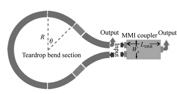
| [31] |
RICARDO C, RAGHUNATHAN V, DIMITROPOULOS D, et al. Influence of nonlinear absorption on Raman amplification in Silicon waveguides[J]. Optics Express, 2004, 12(12):2774-2780. doi: 10.1364/OPEX.12.002774
|
| [32] |
DIMITROPOULOS D, FATHPOUR S, JALALI B. Limitations of active carrier removal in silicon Raman amplifiers and lasers[J]. Applied Physics Letters, 2005, 87(26):261108-3. doi: 10.1063/1.2155071
|
| [33] |
LIU Y, TSANG H K. Nonlinear absorption and Raman gain in helium-ion-implanted silicon waveguides[J]. Optics Letters, 2006, 31(11):1714-1716. doi: 10.1364/OL.31.001714
|
| [34] |
HEWITT P D, REED G T. Improving the response of optical phase modulators in SOI by computer simulation[J]. J. Lightwave Technology, 2000, 18(3):443-450. doi: 10.1109/50.827519
|
| [35] |
GRILLOT F, VIVIEN L, CASSAN E, et al.. Influence of waveguide geometry on scattering loss effects in submicron strip silicon-on-insulator waveguides[J]. IET Optoelectronics, 2008, 2(1):1-5. doi: 10.1049/iet-opt:20070001
|
| [36] |
PAYNE F P, LACEY J P R. A theoretical analysis of scattering loss from planar optical waveguides[J]. Optical & Quantum Electronics, 1994, 26(10):977-986.
|
| [37] |
PAFCHEK R, TUMMIDI R, LI J, et al.. Low-loss silicon-on-insulator shallow-ridge TE and TM waveguides formed using thermal oxidation[J]. Applied Optics, 2009, 48(5):958-963. doi: 10.1364/AO.48.000958
|
| [38] |
LEE K K, LIM D R, KIMERLING L C, et al.. Fabrication of ultralow-loss Si/SiO2 waveguides by roughness reduction[J]. Optics Letters, 2001, 26(23):1888-1890. doi: 10.1364/OL.26.001888
|
| [39] |
LIU H C, LIN Y H, HSU W. Sidewall roughness control in advanced silicon etch process[J]. Microsystem Technologies, 2003, 10(1):29-34. doi: 10.1007/s00542-003-0309-8
|
| [40] |
GAO F, WANG Y, CAO G, et al.. Improvement of sidewall surface roughness in silicon-on-insulator rib waveguides[J]. Applied Physics B, 2005, 81(5):691-694. doi: 10.1007/s00340-005-1951-x
|
| [41] |
CHABLOZ M, SAKAI Y, MATSUURA T, et al. Improvement of sidewall roughness in deep silicon etching[J]. Microsystem Technologies, 2000, 6(3):86-89. doi: 10.1007/s005420050003
|
| [42] |
SNYDER A W. Radiation losses due to variations of radius on dielectric or optical fibers[J]. IEEE Transactions on Microwave Theory and Techniques, 1970, 18(9):608-614. doi: 10.1109/TMTT.1970.1127296
|
| [43] |
LEWIN L. Radiation from curved dielectric slabs and fibers[J]. IEEE Transactions on Microwave Theory & Techniques, 1974, 22(7):718-727.
|
| [44] |
KUESTER E F, CHANG D C. Surface-wave radiation loss from curved dielectric slabs and fibers[J]. IEEE J. Quantum Electronics, 1975, 11(11):903-907. doi: 10.1109/JQE.1975.1068548
|
| [45] |
MARCUSE D. Curvature loss formula for optical fibers[J]. J. Optical Society of America, 1976, 66(3):216-220. doi: 10.1364/JOSA.66.000216
|
| [46] |
MIYAGI M, NISHIDA S. Bending losses of dielectric rectangular waveguides for integrated optics[J]. J. Optical Society of America, 1978, 68(68):316-319. https://www.researchgate.net/publication/243755215_Bending_losses_of_dielectric_rectangular_waveguides_for_integrated_optics
|
| [47] |
WHITE I A. Radiation from bends in optical waveguides:the volume-current method[J]. IEEE J. Microwaves, 1979, 3(5):186-188. doi: 10.1049/ij-moa.1979.0043
|
| [48] |
COLLIN R. Field Theory of Guided Waves[M]. McGraw-Hill, 1960.
|
| [49] |
BRIMONT A, HU X, CUEFF S, et al.. Low-loss and compact silicon rib waveguide bends[J]. IEEE Photonics Technology Letters, 2016, 28(3):299-302. doi: 10.1109/LPT.2015.2495230
|
| [50] |
MITOMI O, KASAYA K, MIYAZAWA H. Design of a single-mode tapered waveguide for low-loss chip-to-fiber coupling[J]. IEEE J. Quantum Electronics, 1994, 30(8):1787-1793. doi: 10.1109/3.301643
|
| [51] |
ALMEIDA V R, PANEPUCCI R R, MICHAL L. Nanotaper for compact mode conversion[J]. Optics Letters, 2003, 28(15):1302-1304. doi: 10.1364/OL.28.001302
|
| [52] |
MARCATILI E A J. Bends in optical dielectric guides[J]. Bell System Technical Journal, 1969, 48(7):2103-2132. doi: 10.1002/bltj.1969.48.issue-7
|
| [53] |
HEIBLUM M, HARRIS J H. Analysis of curved optical-waveguides by conformal transformation[J]. IEEE J. Quantum Electronics, 1975, 11(2):75-83. doi: 10.1109/JQE.1975.1068563
|
| [54] |
CHILWELL J, HODGKINSON I. Thin-films field-transfer matrix theory of planar multilayer waveguides and reflection from prism-loaded waveguides[J]. J. Optical Society of America A Optics & Image Science, 1984, 1(7):742-753. https://www.researchgate.net/publication/239007421_Thin-films_field-transfer_matrix_theory_of_planar_multilayer_waveguides_and_reflection_from_prism-loaded_waveguides
|
| [55] |
THYAGARAJAN K, RAMADAS M R, SHENOY M R. Beat-length measurement of birefringent optical fibers[J]. Optics Letters, 1987, 12(11):935-937. doi: 10.1364/OL.12.000935
|
| [56] |
DAI D X, SAILING H. Analysis of characteristics of bent rib waveguides[J]. J. Optical Society of America A Optics Image Science & Vision, 2004, 21(1):113-121.
|
| [57] |
YAMAMOTO T, KOSHIBA M. Numerical analysis of curvature loss in optical waveguides by the finite-element method[J]. J. Lightwave Technology, 1993, 11(10):1579-1583. doi: 10.1109/50.249899
|
| [58] |
GU J S, BESSE P A, MELCHIOR H. Method of lines for the analysis of the propagation characteristics of curved optical rib waveguides[J]. IEEE J. Quantum Electronics, 1991, 27(3):531-537.
|
| [59] |
FENG N N, ZHOU G R, XU C, et al.. Computation of full-vector modes for bending waveguide using cylindrical perfectly matched layers[J]. J. Lightwave Technology, 2002, 20(11):1976-1980. doi: 10.1109/JLT.2002.806333
|
| [60] |
DAI D X, SHI Y C. Deeply etched SiO2 ridge waveguide for sharp bends[J]. J. Lightwave Technology, 2006, 24(12):5019-5024. doi: 10.1109/JLT.2006.885243
|
| [61] |
HU Z, LU Y Y. Computing optimal waveguide bends with constant width[J]. J. Lightwave Technology, 2007, 25(10):3161-3167. doi: 10.1109/JLT.2007.904033
|
| [62] |
CHERCHI M, YLINEN S, HARJANNE M, et al.. Low-loss spiral waveguides with ultra-small footprint on a micron scale SOI platform[J]. Silicon Photonics Ix, 2014, 8990.
|
| [63] |
ZHUANG L M, MARPAUNG D, BURLA M, et al.. Low-loss, high-index-contrast Si3N4/SiO2 optical waveguides for optical delay lines in microwave photonics signal processing[J]. Optics Express, 2011, 19(23):23162-23170. doi: 10.1364/OE.19.023162
|
| [64] |
HU R, DAI D, HE S. A small polymeric ridge waveguide with a high index contrast[J]. J. Lightwave Technology, 2008, 26(13-16):1964-1968. https://www.researchgate.net/publication/3244617_A_Small_Polymeric_Ridge_Waveguide_With_a_High_Index_Contrast
|
| [65] |
FISCHER U, ZINKE T, KROPP J R, et al.. 0.1 dB/cm waveguide losses in single-mode SOI rib waveguides[J]. IEEE Photonics Technology Letters, 1996, 8(5):647-648. doi: 10.1109/68.491567
|
| [66] |
TANG Y Z, WANG W H, LI T, et al. Integrated waveguide turning mirror in silicon-on-insulator[J]. Photonics Technology Letters IEEE, 2002, 14(1):68-70. doi: 10.1109/68.974164
|
| [67] |
CHERCHI M, YLINEN S, HARJANNE M, et al.. Dramatic size reduction of waveguide bends on a micron-scale silicon photonic platform[J]. Optics Express, 2013, 21(15):17814-17823. doi: 10.1364/OE.21.017814
|
| [68] |
ERIC D, FENGNIAN X, LAURENT S, et al.. Group index and group velocity dispersion in silicon-on-insulator photonic wires[J]. Optics Express, 2006, 14(9):3853-3863. doi: 10.1364/OE.14.003853
|
| [69] |
MUSA S, BORREMAN A, KOK A A M, et al.. Experimental study of bent multimode optical waveguides[J]. Annals of Surgery,1984, 200(2):153-158. doi: 10.1097/00000658-198408000-00006
|
| [70] |
HARJANNE M, AALTO T. Design of tight bends in silicon-on-insulator ridge waveguides[J]. Physica Scripta, 2004, T114:209-212. doi: 10.1088/0031-8949/2004/T114/053
|
| [71] |
AALTO T, CHERCHI M, HARJANNE M, et al.. Launching of multi-project wafer runs in ePIXfab with micron-scale silicon rib waveguide technology[J]. Silicon Photonics Ⅸ, 2014, 8990.
|
| [72] |
SOLEHMAINEN K, AALTO T, DEKKER J, et al. Development of multi-step processing in silicon-on-insulator for optical waveguide applications[J]. J. Optics a-Pure and Applied Optics, 2006, 8(7):S455-S460. doi: 10.1088/1464-4258/8/7/S22
|
| [73] |
SOREF R A, SCHMIDTCHEN J, PETERMANN K. Large single-mode rib waveguides in GeSi-Si and Si-on-SiO2[J]. Quantum Electronics IEEE J., 1991, 27(8):1971-1974. doi: 10.1109/3.83406
|
| [74] |
DULLO F T, TINGUELY J C, SOLBO S A, et al.. Single-mode limit and bending losses for shallow rib Si3N4 waveguides[J]. IEEE Photonics J., 2015, 7(1):2700511-10. https://www.researchgate.net/profile/Stian_Solbo/publication/273166722_Single-Mode_Limit_and_Bending_Losses_for_Shallow_Rib_Si3N4_Waveguides/links/552cdea60cf2e089a3acfc02.pdf?origin=publication_detail
|
| [75] |
DAY I E, EVANS I, KNIGHTS A, et al.. Tapered silicon waveguides for low insertion loss highly-efficient high-speed electronic variable optical attenuators[C]. Optical Fiber Communications Conference, 2003. OFC 2003, 2003:249-251.
|
| [76] |
ANITA S, THOMAS D, JANUSZ M, et al.. Fabrication and characterization of three-dimensional silicon tapers[J]. Optics Express, 2003, 11(26):3555-3561. doi: 10.1364/OE.11.003555
|
| [77] |
SMIT M K, PENNINGS E C M, BLOK B. Normalized approach to the design of low-loss optical waveguide bends[J]. J. Lightwave Technology, 1993, 11(11):1737-1742. doi: 10.1109/50.251169
|
| [78] |
NGUYEN T G, TUMMIDI R S, KOCH T L, et al.. Lateral leakage of TM-like mode in thin-ridge silicon-on-insulator bent waveguides and ring resonators[J]. Optics Express, 2010, 18(7):7243-7252. doi: 10.1364/OE.18.007243
|
| [79] |
ZHANG X M, HARRISON M, HARKER A, et al.. Serpentine low loss trapezoidal silica waveguides on silicon[J]. Optics Express, 2012, 20(20):22298-22307. doi: 10.1364/OE.20.022298
|
| [80] |
MANOLATOU C, JOHNSON S G, FAN S, et al. High-density integrated optics[J]. J. Lightwave Technology, 1999, 17(9):1682-1692. doi: 10.1109/50.788575
|
| [81] |
HOCHBERG M, BAEHRJONES T. Towards fabless silicon photonics[J]. Nature Photonics, 2010, 4(8):492-494. doi: 10.1038/nphoton.2010.172
|
| [82] |
PO D, WEI Q, HONG L, et al.. Low power and compact reconfigurable multiplexing devices based on silicon microring resonators[J]. Optics Express, 2010, 18(10):9852-9858. doi: 10.1364/OE.18.009852
|
| [83] |
NEUMANN E G. Curved Dielectric Optical Waveguide with Reduced Transition Losses[J]. Microwaves Antennas & Propagation, 1982, 129(5):278-280.
|
| [84] |
SMIT M K, PENNINGS E C M, BLOK H. A normalized approach to the design of low-loss optical wave-guide bends[J]. J. Lightwave Technology, 1993, 11(11):1737-1742. doi: 10.1109/50.251169
|
| [85] |
PENNINGS E C M. Bends in optical ridge waveguides:modeling and experiments[D]. Netherland:Delft University of Technology, 1990.
|
| [86] |
FAN G, SANG W, LIU X, et al.. Silicon waveguide racetrack resonators with 1.5μm radius using junction offsets[J]. Microwave & Optical Technology Letters, 2012, 54(6):1470-1471.
|
| [87] |
CHEN T, LEE H, LI J, et al. A general design algorithm for low optical loss adiabatic connections in waveguides[J]. Optics Express, 2012, 20(20):22819-22829. doi: 10.1364/OE.20.022819
|
| [88] |
CAI D P, LU J H, CHEN C C, et al. High Q-factor microring resonator wrapped by the curved waveguide[J]. Scientific Reports, 2015, 5. https://www.researchgate.net/publication/277084453_High_Q-factor_microring_resonator_wrapped_by_the_curved_waveguide
|
| [89] |
LAI C H, CHANG T, YEH Y S. Characteristics of bent terahertz antiresonant reflecting pipe waveguides[J]. Optics Express, 2014, 22(7):8460-8472. doi: 10.1364/OE.22.008460
|
| [90] |
MELLONI A, MONGUZZI P, COSTA R, et al.. Design of curved waveguides:the matched bend[J]. J. Optical Society of America a-Optics Image Science and Vision, 2003, 20(1):130-137. doi: 10.1364/JOSAA.20.000130
|
| [91] |
YUAN W, HALL D C. A General Scaling Rule for Matched Bend Waveguides[J]. J. Lightwave Technology, 2011, 29(24):3786-3796. doi: 10.1109/JLT.2011.2174335
|
| [92] |
YUAN W, SEIBERT C S, HALL D C. Single-facet teardrop laser with matched-bends design[J]. IEEE J. Selected Topics in Quantum Electronics, 2011, 17(6):1662-1669. doi: 10.1109/JSTQE.2011.2111360
|
| [93] |
LEE H, CHEN T, LI J, et al.. Chemically etched ultrahigh-Q wedge-resonator on a silicon chip[J]. Nature Photonics, 2012, 6(6):369-373. doi: 10.1038/nphoton.2012.109
|
| [94] |
CHEN T, LEE H, VAHALA K J. Design and characterization of whispering-gallery spiral waveguides[J]. Optics Express, 2014, 22(5):5196-5208. doi: 10.1364/OE.22.005196
|
| [95] |
SHEEHAN R N, HORNE S, PETERS F H. The design of low-loss curved waveguides[J]. Optical and Quantum Electronics, 2008, 40(14-15):1211-1218. doi: 10.1007/s11082-009-9329-7
|
| [96] |
BAETS R, LAGASSE P E. Loss calculation and design of arbitrarily curved integrated-optic waveduides[J]. J. Optical Society of America, 1983, 73(2):177-182. doi: 10.1364/JOSA.73.000177
|
| [97] |
DAI D X. Multimode optical waveguide enabling microbends with low inter-mode crosstalk for mode-multiplexed optical interconnects[J]. Optics Express, 2014, 22(22):27524-27534. doi: 10.1364/OE.22.027524
|
| [98] |
KRAUSE M, RENNER H, BRINKMEYER E. Polarization-dependent curvature loss in silicon rib waveguides[J]. IEEE J. Selected Topics in Quantum Electronics, 2006, 12(6):1359-1362. doi: 10.1109/JSTQE.2006.884068
|
| [99] |
DAOXIN D, BOWERS J E. Novel concept for ultracompact polarization splitter-rotator based on silicon nanowires[J]. Optics Express, 2011, 19(11):10940-10949. doi: 10.1364/OE.19.010940
|
| [100] |
VERMEULEN D, ACOLEYEN K V, GHOSH S, et al.. Efficient tapering to the fundamental quasi-TM mode in asymmetrical waveguides[C]. 15th European conference on Integrated Optics (ECIO 2010), 2010.
|
| [101] |
CHERCHI M, YLINEN S, HARJANNE M, et al.. The Euler bend:paving the way for high-density integration on micron-scale semiconductor platforms[J]. Silicon Photonics Ix, 2014, 8990. http://proceedings.spiedigitallibrary.org/pdfaccess.ashx?url=/data/conferences/spiep/78713/899004.pdf
|
| [102] |
MEKIS A, CHEN J C, KURLAND I I, et al.. High transmission through sharp bends in photonic crystal waveguides[J]. Physical Review Letters, 1996, 77(18):3787-3790. doi: 10.1103/PhysRevLett.77.3787
|
| [103] |
BOGAERTS W, BAETS R, DUMON P, et al. Nanophotonic waveguides in silicon-on-insulator fabricated with CMOS technology[J]. J. Lightwave Technology, 2005, 23(1):401-412. doi: 10.1109/JLT.2004.834471
|
| [104] |
ALMEIDA V R, QIANFAN X, BARRIOS C A, et al.. Guiding and confining light in void nanostructure[J]. Optics Letters, 2004, 29(11):1209-1211. doi: 10.1364/OL.29.001209
|
| [105] |
KOOS C, VORREAU P, VALLAITIS T, et al.. All-optical high-speed signal processing with silicon-organic hybrid slot waveguides[J]. Nature Photonics, 2009, 3(4):216-219. doi: 10.1038/nphoton.2009.25
|
| [106] |
JUNG E J, LEE W J, KIM M J, et al.. Design of hybrid optical waveguide with a 90A degrees bend structure for high density photonics integrated circuits[J]. Optical and Quantum Electronics, 2013, 45(7):721-726. doi: 10.1007/s11082-012-9633-5
|
| [107] |
CLAUDIO D, THEO L, MARTIN O J F, et al.. Simulation of complex plasmonic circuits including bends[J]. Optics Express, 2011, 19(20):18979-18988. doi: 10.1364/OE.19.018979
|
| [108] |
管小伟, 吴昊, 戴道锌.硅基混合表面等离子体纳米光波导及集成器件[J].中国光学, 2014, (2):181-195. http://www.chineseoptics.net.cn/CN/abstract/abstract9117.shtml
GUAN X W, WU H, DAI D X. Silicon hybrid surface plasmonic nano-optics-waveguide and integration devices[J]. Chinese Optics, 2014, (2):181-195. http://www.chineseoptics.net.cn/CN/abstract/abstract9117.shtml
|
| [109] |
ZHOU X, ZHANG T, CHEN L, et al.. A Graphene-based hybrid plasmonic waveguide with ultra-deep subwavelength confinement[J]. J. Lightwave Technology, 2014, 32(21):4199-4203. doi: 10.1109/JLT.2014.2350487
|
| [110] |
DAOXIN D, SAILING H. A silicon-based hybrid plasmonic waveguide with a metal cap for a nano-scale light confinement[J]. Optics Express, 2009, 17(19):16646-16653. doi: 10.1364/OE.17.016646
|
| [111] |
CHEN P X, ZHU Y P, SHI Y C, et al.. Fabrication and characterization of suspended SiO2 ridge optical waveguides and the devices[J]. Optics Express, 2012, 20(20):22531-22536. doi: 10.1364/OE.20.022531
|
| [112] |
LI L X, NORDIN G P, ENGLISH J M, et al.. Integrated Optics:Devices, Materials, and Technologies Ⅶ[M]. SPIE, 2003.
|
| [113] |
CASSAN E, VIVIEN L, LAVAL S. Polarization-independent 90 degrees-turns in single-mode micro-waveguides on silicon-on-insulator wafers for telecommunication wavelengths[J]. Optics Communications, 2004, 235(1-3):83-88. doi: 10.1016/j.optcom.2004.02.080
|
| [114] |
QIAN Y, KIM S, SONG J, et al.. Compact and low loss silicon-on-insulator rib waveguide 90 degrees bend[J]. Optics Express, 2006, 14(13):6020-6028. doi: 10.1364/OE.14.006020
|
| [115] |
XIAO S J, KHAN M H, SHEN H, et all. Modeling and measurement of losses in silicon-on-insulator resonators and bends[J]. Optics Express, 2007, 15(17):10553-10561. doi: 10.1364/OE.15.010553
|
| [116] |
DAI DX. Subwavelength silica-based optical waveguide with a multilayered buffer for sharp bending[J]. Jl Lightwave Technology, 2009, 27(13):2489-2494. doi: 10.1109/JLT.2008.2011501
|
| [117] |
LUO J, XU P, CHEN H, et al. Realizing almost perfect bending waveguides with anisotropic epsilon-near-zero metamaterials[J]. Applied Physics Letters, 2012, 100(22):221903-221903-221905. doi: 10.1063/1.4723844
|
| [118] |
FU Y, XU Y, CHEN H. Applications of gradient index metamaterials in waveguides[J]. Scientific Reports, 2015, 5. https://www.researchgate.net/publication/286982878_Applications_of_gradient_index_metamaterials_in_waveguides/fulltext/56953d3708aeab58a9a4d7d0/286982878_Applications_of_gradient_index_metamaterials_in_waveguides.pdf
|
| [119] |
李浩, 宋玲玲, 张立钧等.4通道交叉型二氧化硅光波导延迟线阵列的设计与制备[J].中国光学, 2014, (3):435-441. http://www.chineseoptics.net.cn/CN/abstract/abstract9143.shtml
LI H, SONG L L, ZHANG L J, et al.. Design and fabrication of 4 channels silica cross optical waveguide delay line array[J]. Chinese Optics, 2014, (3):435-441. http://www.chineseoptics.net.cn/CN/abstract/abstract9143.shtml
|
| [120] |
RASRAS M S, MADSEN C K, CAPPUZZO M A, et al.. Integrated resonance-enhanced variable optical delay lines[J]. IEEE Photonics Technology Letters, 2005, 17(4):834-836. doi: 10.1109/LPT.2005.844009
|
| [121] |
DENSMORE A, XU D X, JANZ S, et al.. Spiral-path high-sensitive silicon photonic wire molecular sensor with temperature-independent response[J]. Optics Letters, 2008, 33(6):596-598. doi: 10.1364/OL.33.000596
|
| [122] |
CIMINELLI C, DELLOLIO F, ARMENISE M N. High-Q spiral resonator for optical gyroscope applications:numerical and experimental investigation[J]. IEEE Photonics J., 2012, 4(4):1844-1854. https://www.researchgate.net/publication/233979298_High-Q_Spiral_Resonator_for_Optical_Gyroscope_Applications_Numerical_and_Experimental_Investigation
|
| [123] |
CHAN H P, CHENG S Y, CHUNG P S. Low loss wide-angle symmetric Y-branch waveguide[J]. Electronics Letters, 1996, 32(7):652-654. doi: 10.1049/el:19960452
|
| [124] |
QIAN W, JUN L, SAILING H. Optimal design method of a low-loss broadband Y branch with a multimode waveguide section[J]. Applied Optics, 2003, 41(36):7644-7649. https://www.researchgate.net/publication/10965541_Optimal_design_method_of_a_low-loss_broadband_Y_branch_with_a_multimode_waveguide_section
|
| [125] |
CHERCHI M, YLINEN S, HARJANNE M, et al.. Fabrication-tolerant optical filters for dense integration on a micron-scale SOI platform[J]. Silicon Photonics Ⅸ, 2014:8990. https://www.researchgate.net/publication/262982534_Fabrication-tolerant_optical_filters_for_dense_integration_on_a_micron-scale_SOI_platform
|
| [126] |
XIAO S J, KHAN M H, SHEN H, et al.. Compact silicon microring resonators with ultra-low propagation loss in the C band[J]. Optics Express, 2007, 15(22):14467-14475. doi: 10.1364/OE.15.014467
|
| [127] |
XIAO S, KHAN M H, SHEN H, et al.. Silicon-on-insulator microring add-drop filters with free spectral ranges over 30 nm[J]. J. Lightwave Technology, 2008, 26(2):228-236. doi: 10.1109/JLT.2007.911098
|
| [128] |
LI X B, DENG Q Z, ZHOU Z P. Low loss, high-speed single-mode half-disk resonator[J]. Optics Letters, 2014, 39(13):3810-3813. doi: 10.1364/OL.39.003810
|
| [129] |
BIAN Z X, LIU B, SHAKOURI A. InP-based passive ring-resonator-coupled lasers[J]. IEEE J. Quantum Electronics, 2003, 39(7):859-865. doi: 10.1109/JQE.2003.813222
|
| [130] |
KIM K C, HAN I K, LEE J I, et al.. High power single-lateral-mode operation of InAs quantum dot based ridge type laser diodes by utilizing a double bend waveguide structure[J]. Applied Physics Letters, 2010, 96(26):261103-261106. doi: 10.1063/1.3458704
|
| [131] |
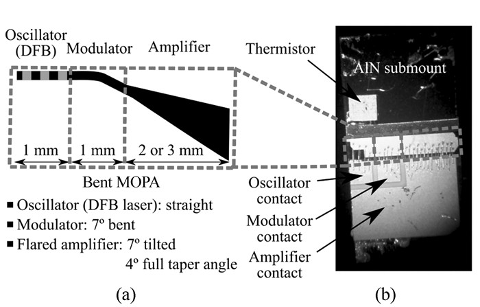
FAUGERON M, VILERA M, KRAKOWSKI M, et al.. High power three-section integrated master oscillator power amplifier at 1.5μm[J]. IEEE Photonics Technology Letters, 2015, 27(13):1449-1452. doi: 10.1109/LPT.2015.2425534
|
| [132] |
GUAN X, WU H, SHI Y, et al.. Extremely small polarization beam splitter based on a multimode interference coupler with a silicon hybrid plasmonic waveguide[J]. Optics Letters, 2014, 39(2):259-262. doi: 10.1364/OL.39.000259
|
| [133] |
UEMATSU T, KITAYAMA T, ISHIZAKA Y, et al.. Ultra-broadband silicon-wire polarization beam combiner/splitter based on a wavelength insensitive coupler with a point-symmetrical configuration[J]. IEEE Photonics J., 2014, 6(1):1-8. https://www.researchgate.net/publication/260521192_Ultra-Broadband_Silicon-Wire_Polarization_Beam_CombinerSplitter_Based_on_a_Wavelength_Insensitive_Coupler_With_a_Point-Symmetrical_Configuration
|
| [134] |
SHRESTHA V R, LEE H S, LEE Y G, et al.. Silicon nitride waveguide router enabling directional power transmission[J]. Optics Communications, 2014, 331(22):64-68. http://adsabs.harvard.edu/abs/2014OptCo.331...64S
|
| [135] |
ZHOU K, WEI W, ZHANG C. Simulation on a novel SOI optical waveguide directional coupler[J]. SPIE, 2003, 5253:897-900. https://www.researchgate.net/publication/242241375_Simulation_on_a_novel_SOI_optical_waveguide_directional_coupler
|
| [136] |
JONS K D, RENGSTL U, OSTER M, et al.. Monolithic on-chip integration of semiconductor waveguides, beamsplitters and single-photon sources[J]. J. Physics D-Applied Physics, 2015, 48(8):7-20. https://www.researchgate.net/publication/261182152_Monolithic_on-chip_integration_of_semiconductor_waveguides_beamsplitters_and_single-photon_sources
|
Figures(13)


 DownLoad: