| Citation: | BIAN Xiao-yue, HAN Sen, WU Quan-ying. Interferometry of double-sided polished wafer and error analysis[J]. Chinese Optics, 2023, 16(4): 916-932. doi: 10.37188/CO.2022-0226

|
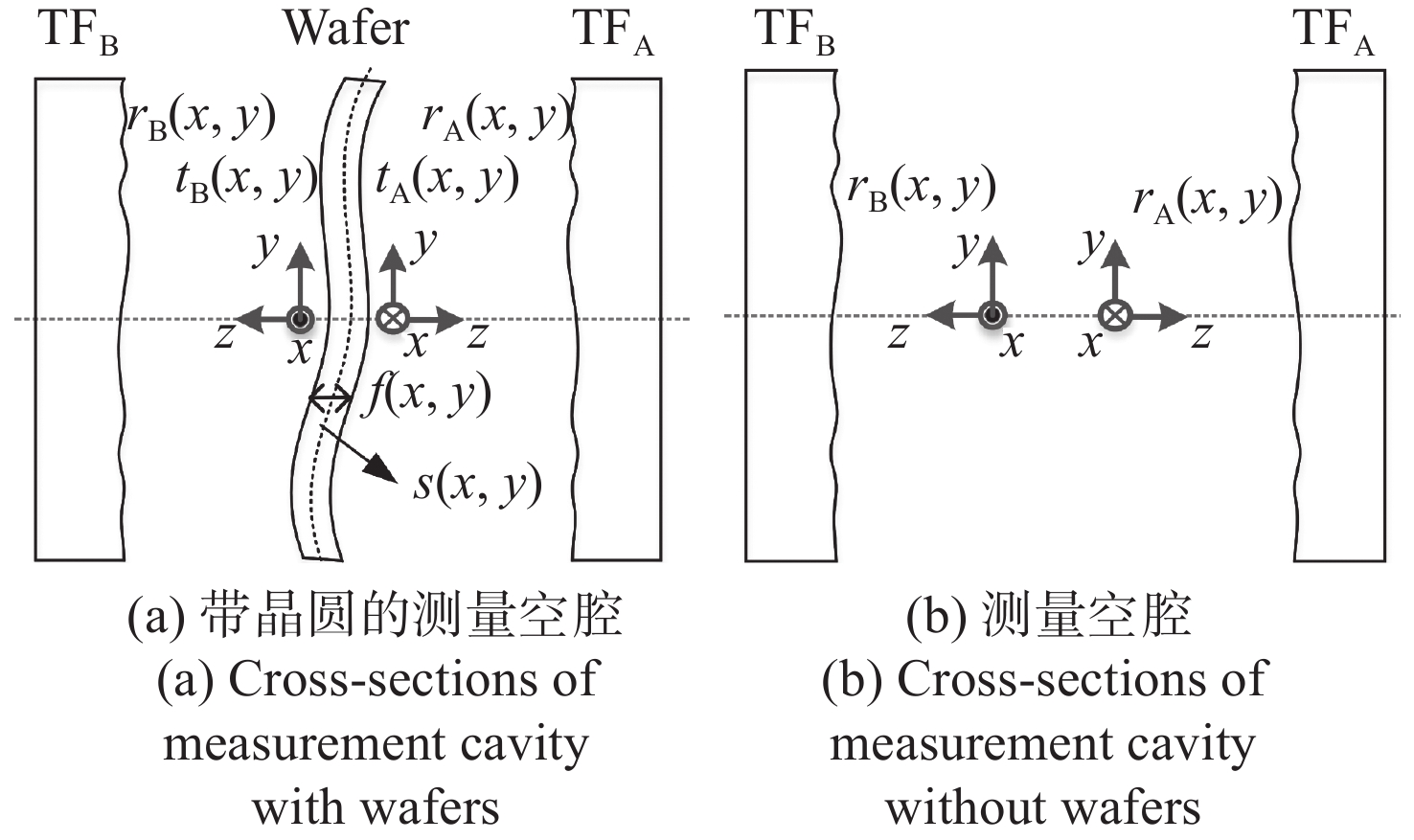
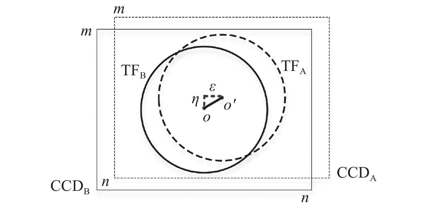
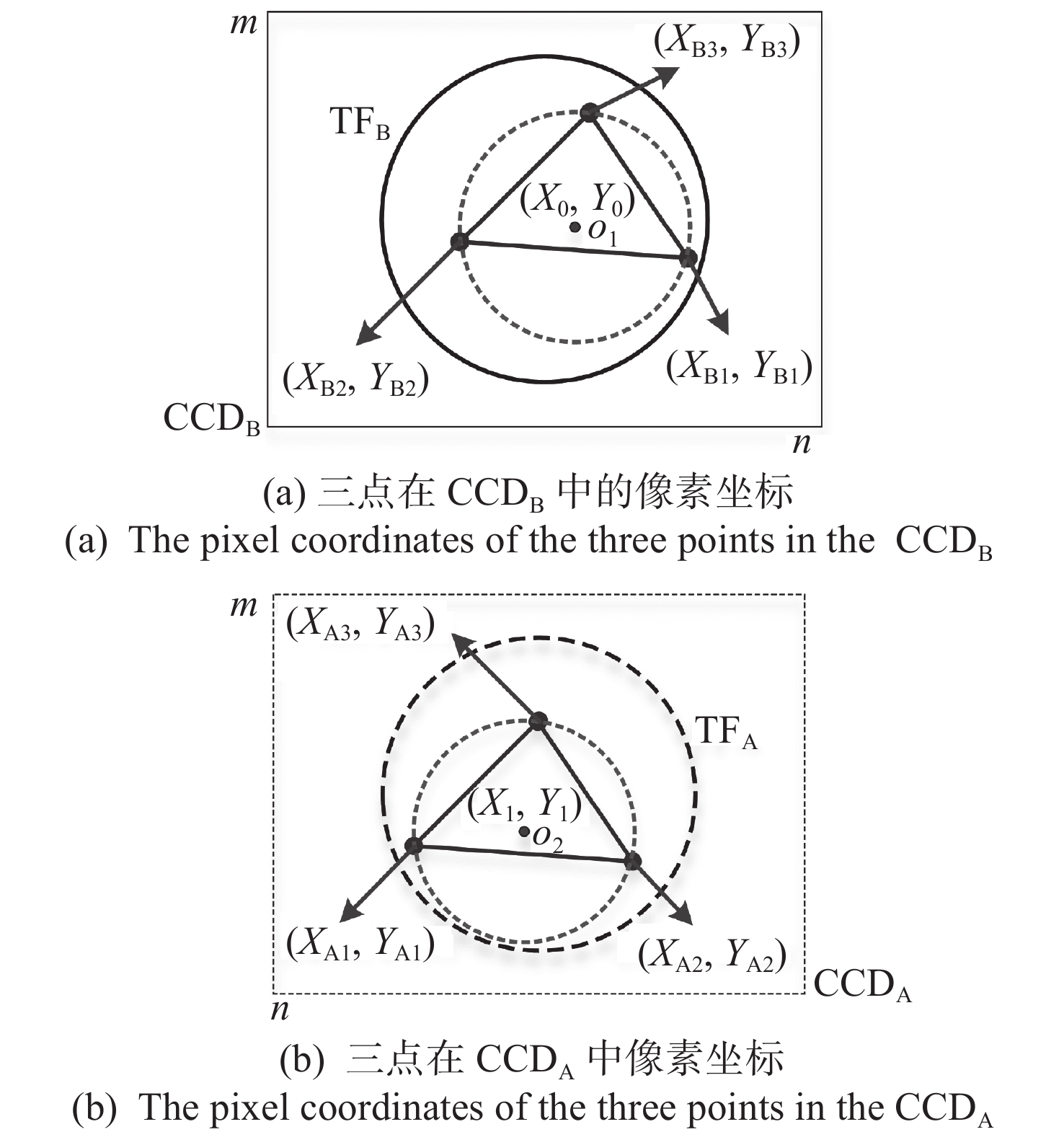
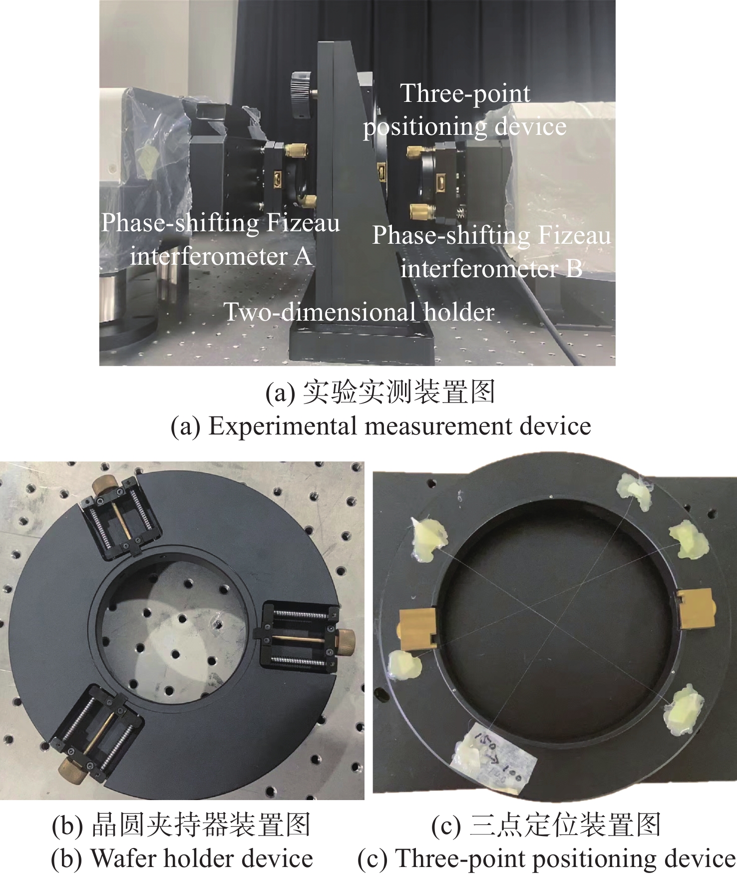
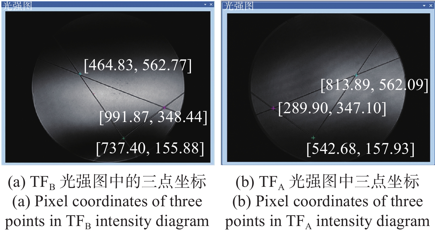
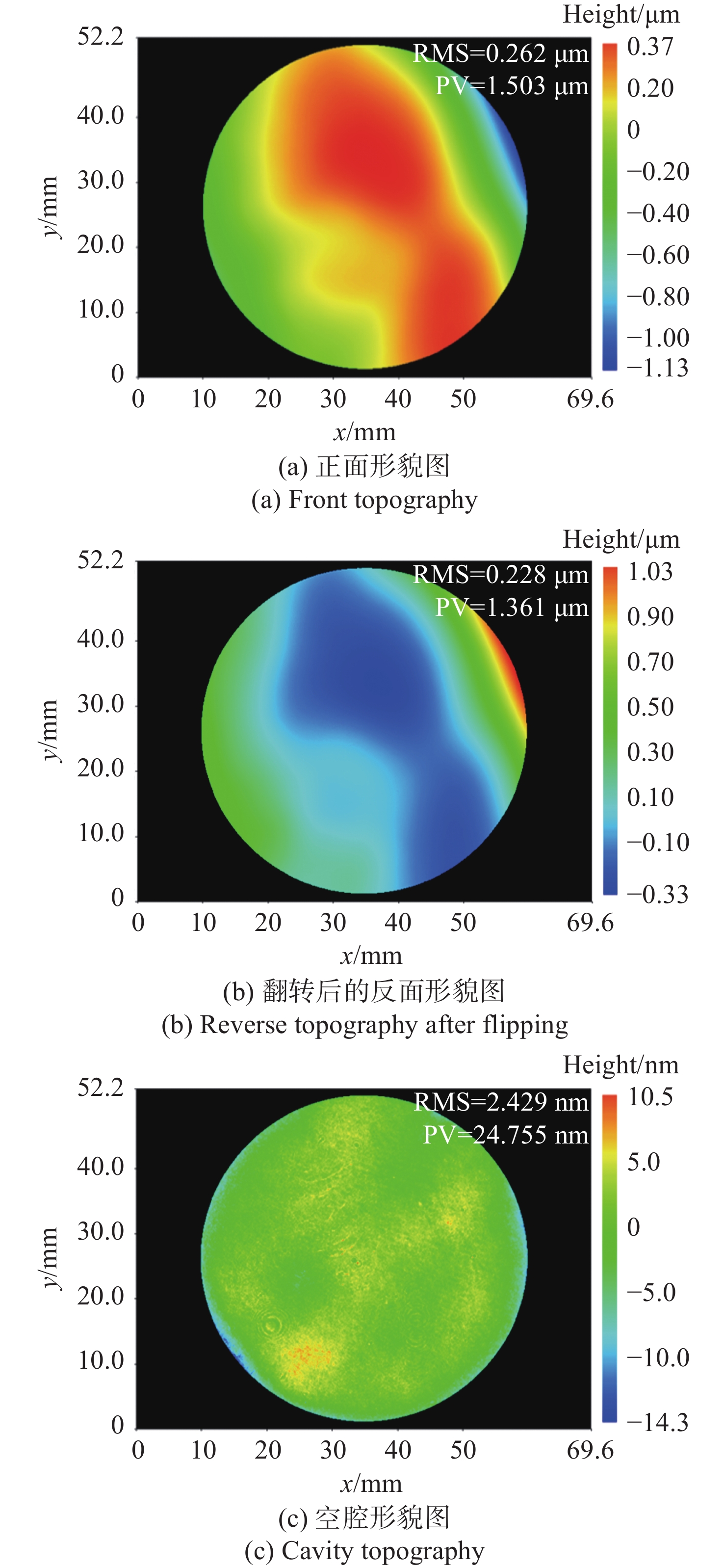
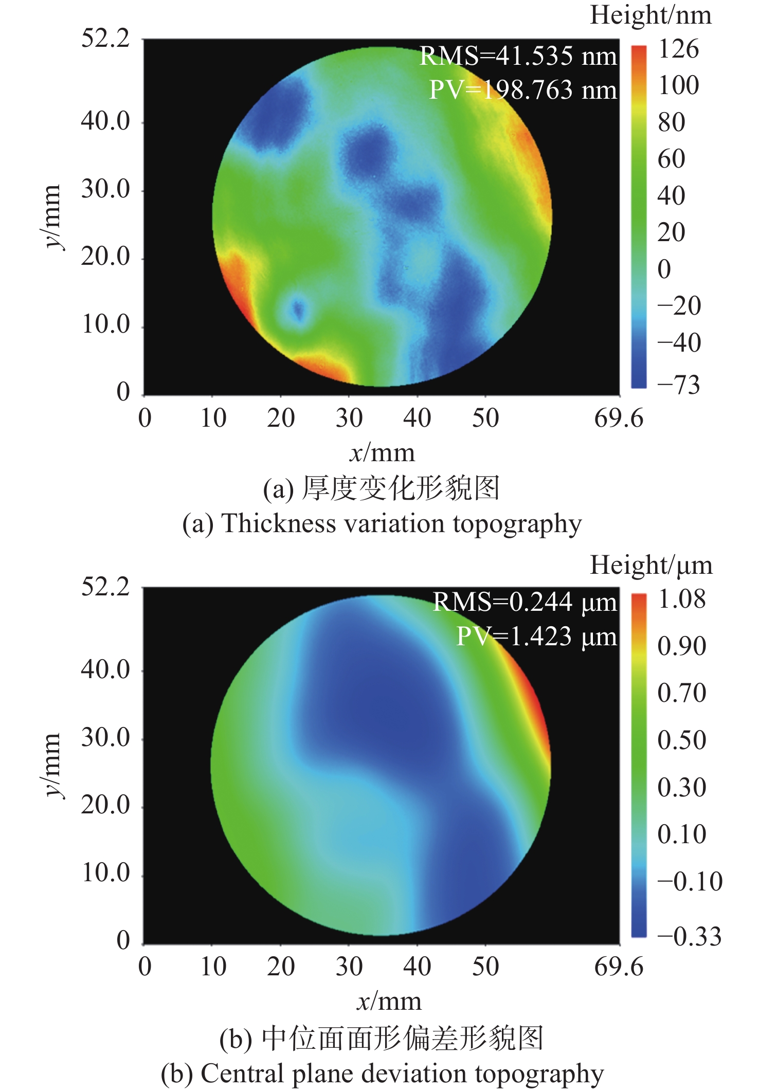
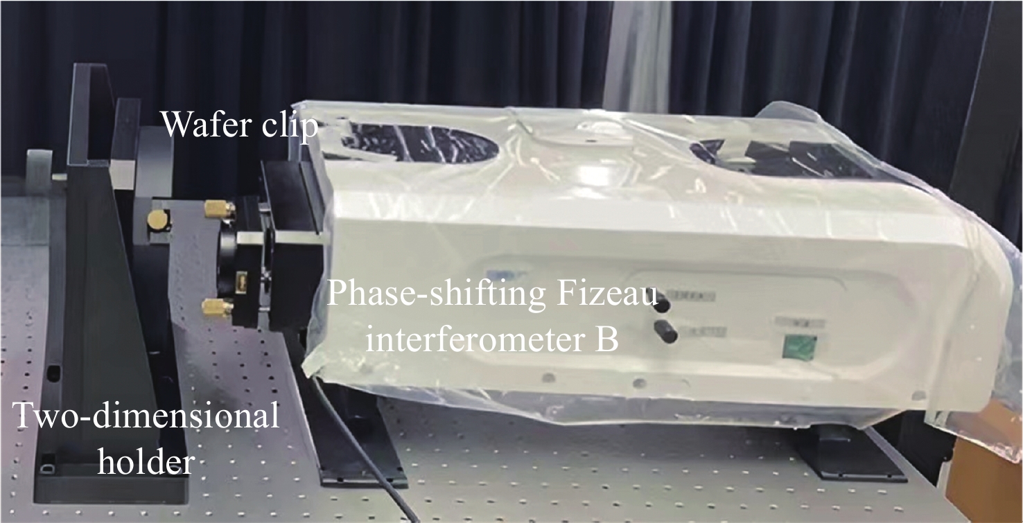
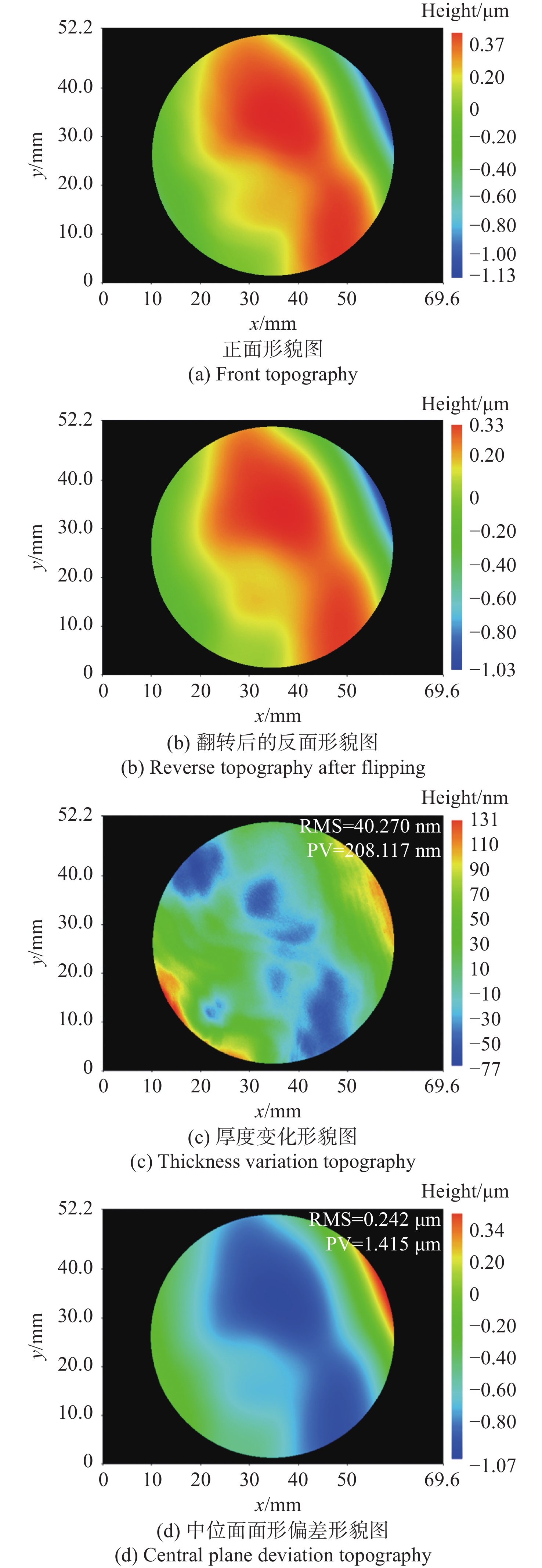
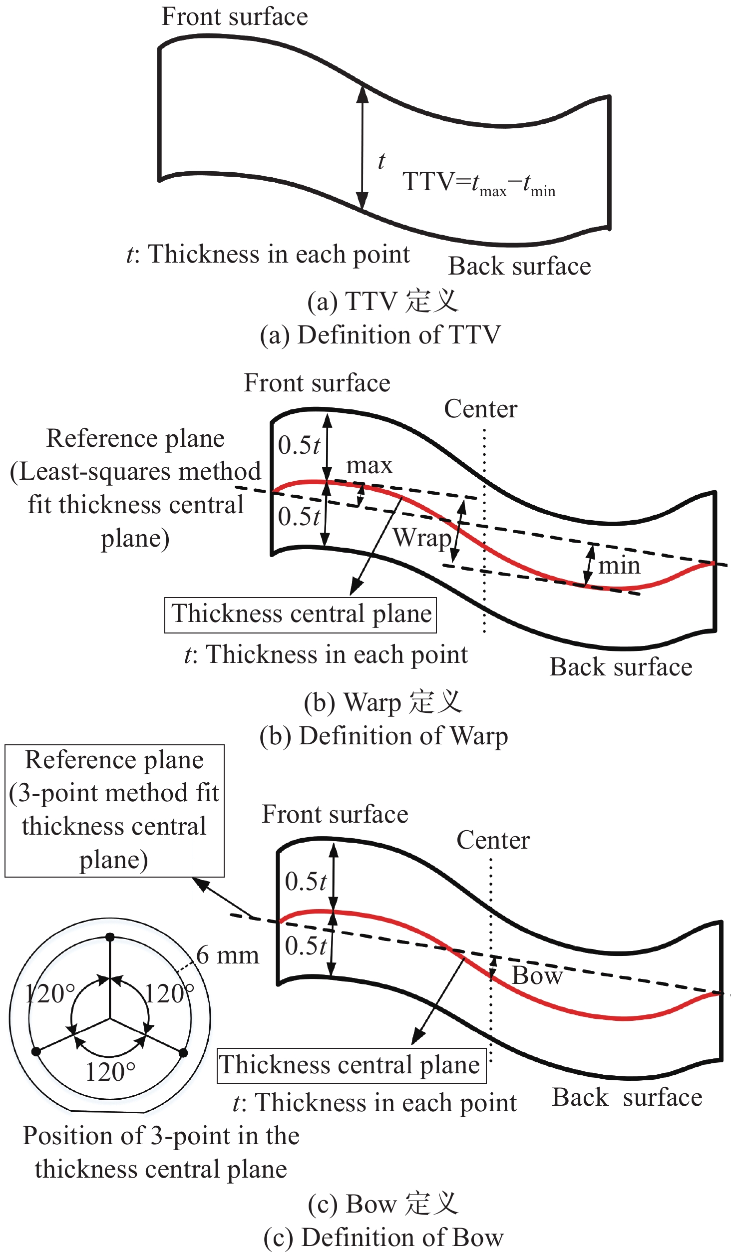
An interferometric measurement method is proposed to measure the Total Thickness Variation (TTV) and the Bow and Warp in the deformation of a double-sided polished wafer. Two phase-shifting Fizeau interferometers with reference mirrors are used to measure the topography of the front and back surfaces of the wafer simultaneously, and the measured topography of the front and back surfaces of the wafer are combined with the cavity topography of the two interferometers when the wafer is not placed to obtain the surface parameters of the double-sided polished wafer which are not affected by the reference mirror error. In the combined operation, the mapping error is introduced because the two reference mirrors are not precisely aligned, which affects the measurement results of the relevant parameters. To this end, before wafer measurement, the three-point positioning device is fixed between the two reference mirrors, and the position of the two reference mirrors is continuously adjusted based on the three-point circular theorem, which can make the mapping error extremely small, thereby reducing the influence of the mapping error on the measurement results. The experimental results show that the mapping errors of 50 mm wafer transverse and longitudinal directions are 21.592 μm and 37.480 μm, respectively, and the TTV, Bow and Warp are 0.198 μm, −0.326 μm and 1.423 μm, respectively. In order to further verify the effectiveness of the adjustment method, a single interferometer was used to flip the wafer for measurement, and the TTV, Bow and Warp of wafer are 0.208 μm, −0.326 μm and 1.415 μm, respectively. The proposed interferometric method can be easily and quickly used for the measurement of large quantities of large-sized wafers after adjusting the position of two reference mirrors, which improves wafer inspection efficiency. At the same time, it has a superior measurement accuracy.

| [1] |
WANG Y M, SHU H W, HAN X Y. High-precision silicon-based integrated optical temperature sensor[J]. Chinese Optics, 2021, 14(6): 1355-1361. (in Chinese) doi: 10.37188/CO.2021-0054
|
| [2] |
HU S Q, TIAN R J, GAN X T. Two-dimensional material photodetector for hybrid silicon photonics[J]. Chinese Optics, 2021, 14(5): 1039-1055. (in Chinese) doi: 10.37188/CO.2021-0003
|
| [3] |
JIANG CH W, SHA Y Q, YUAN J L, et al. Fabrication and characterization of an LED based on a GaN-on-silicon platform with an ultra-thin freestanding membrane in the blue range[J]. Chinese Optics, 2021, 14(1): 153-162. (in Chinese) doi: 10.37188/CO.2020-0148
|
| [4] |
YANG H N, LI K, CHU D P. Liquid crystal on silicon technology and reconfigurable all-optical networks[J]. Chinese Journal of Liquid Crystals and Displays, 2021, 36(6): 772-788. (in Chinese) doi: 10.37188/CJLCD.2021-0014
|
| [5] |
CHEN C F, ZHANG T M, WANG Z L, et al. Annealing effect on photoluminescence in silicon quantum dots prepared by nanosecond pulsed laser[J]. Chinese Journal of Liquid Crystals and Displays, 2022, 37(6): 703-708. (in Chinese)
|
| [6] |
XU Y, Qi P H, HUANG R, et al. Influence of MOS transistor size on data writing in digital driving pixel circuit of OLED-on-silicon[J]. Chinese Journal of Liquid Crystals and Displays, 2021, 36(5): 680-686. (in Chinese) doi: 10.37188/CJLCD.2020-0357
|
| [7] |
IEEE. International roadmap for devices and systemsTM 2021 edition metrology[EB/OL]. USA: IEEE, 2021[2022-12-01].https://irds.ieee.org/images/files/pdf/2021/2021IRDS_MET.pdf.
|
| [8] |
CHEN M Y, PANG SH L, ZHOU J L, et al. High-accuracy spectral interferometer with multi-Fabry-Perot Etalon for thickness measurement of the silicon wafer[J]. Optics Communications, 2021, 501: 127346. doi: 10.1016/j.optcom.2021.127346
|
| [9] |
OH H S, LEE H L. A comparative study between total thickness variance and site flatness of polished silicon wafer[J]. Japanese Journal of Applied Physics, 2001, 40(9R): 5300. doi: 10.1143/JJAP.40.5300
|
| [10] |
MYRONOV M, COLSTON G, DAVIES J, et al. A fast approach to measuring the thickness uniformity of a homoepilayer grown on to any type of silicon wafer[J]. Semiconductor Science and Technology, 2022, 37(6): 065003. doi: 10.1088/1361-6641/ac5f69
|
| [11] |
TAHARA K, MATSUOKA H, KANNAKA M, et al. Wafer flatness measurement system with sub-nanometer precision cancelling the noise caused by a light source using dual heterodyne interferometer[J]. Journal of the Society of Materials Science, 2018, 67(9): 829-833. doi: 10.2472/jsms.67.833
|
| [12] |
FREISCHLAD K, TANG SH H, GRENFELL J. Interferometry for wafer dimensional metrology[J]. Proceedings of SPIE, 2007, 6672: 667202. doi: 10.1117/12.732546
|
| [13] |
杨梦柯. WLCSP封装晶圆翘曲成因与控制方法研究[D]. 北京: 北京工业大学, 2019.
YANG M K. The study on wafer warpage and controlling strategies for WLCSP[D]. Beijing: Beijing University of Technology, 2019. (in Chinese)
|
| [14] |
JANSEN M J, HAITJEMA H, SCHELLEKENS P H J. Scanning wafer thickness and flatness interferometer[J]. Proceedings of SPIE, 2004, 5252: 334-345. doi: 10.1117/12.515650
|
| [15] |
TAHARA K, MATSUOKA H, MORIOKA N, et al. Determination of silicon wafer site flatness using dual heterodyne interferometers with sub-nanometer precision[J]. Review of Scientific Instruments, 2020, 91(6): 065114. doi: 10.1063/1.5143534
|
| [16] |
PARK J, BAE J, JANG Y S, et al. A novel method for simultaneous measurement of thickness, refractive index, bow, and warp of a large silicon wafer using a spectral-domain interferometer[J]. Metrologia, 2020, 57(6): 064001. doi: 10.1088/1681-7575/aba16b
|
| [17] |
松岡英毅, 山本雄治, 綱木英俊, 等. ウェーハの形状, 平担度測定装置[J]. R&D神戸製鋼技報, 2009, 59(2): 7-11.
MATSUOKA H, YAMAMOTO Y, TSUNAKI H, et al. . Wafer shape and flatness measurement system Shapes and flatness measurement system of silicon wafer[J]. R&D Kobe Steel Engineering Reports, 2009, 59(2): 7-11. (in Japanese)
|
| [18] |
陈建强, 曾安, 唐寿鸿. 哈特曼测量装置及其测量方法和晶圆几何参数测量装置: 中国, 114543695A[P]. 2022-05-27.
CHEN J Q, ZENG A, TANG SH H. Hartmann measurement device and its measurement method and wafer geometry parameter measurement device: CN, 114543695A[P]. 2022-05-27. (in Chinese)
|
| [19] |
赵智亮, 陈立华, 赵子嘉, 等. 一种立式半导体晶圆TTV干涉测试装置: 中国, 215064363U[P]. 2021-12-07.
ZHAO ZH L, CHEN L H, ZHAO Z J, et al. . A vertical semiconductor wafer TTV interference test device: CN, 215064363U[P]. 2021-12-07. (in Chinese)
|
| [20] |
中华人民共和国国家质量监督检验检疫总局, 中国国家标准化管理委员会. GB/T 29507-2013 硅片平整度、厚度及总厚度变化测试 自动非接触扫描法[S]. 北京: 中国标准出版社, 2013.
General Administration of Quality Supervision, Inspection and Quarantine of the People's Republic of China, Standardization Administration of the People's Republic of China. GB/T 29507-2013 Test method for measuring flatness, thickness and total thickness variation on silicon wafers—Automated non-contact scanning[S]. Beijing: Standards Press of China, 2013. (in Chinese)
|
| [21] |
国家市场监督管理总局, 国家标准化管理委员会. GB/T 32280-2022 硅片翘曲度和弯曲度的测试 自动非接触扫描法[S]. 北京: 中国标准出版社, 2022.
State Administration for Market Regulation, Standardization Administration of the People's Republic of China. GB/T 32280-2022 Test method for warp and bow of silicon wafers—Automated non-contact scanning method[S]. Beijing: Standards Press of China, 2022. (in Chinese)
|
Figures(11)


 DownLoad: