| Citation: | XIE Bing, AN Xu-hong, ZHAO Wei-wei, NI Zhen-hua. Recent progress on synthesis and optical characterization of two-dimensional Bi2O2Se[J]. Chinese Optics, 2023, 16(1): 24-43. doi: 10.37188/CO.2022-0071

|
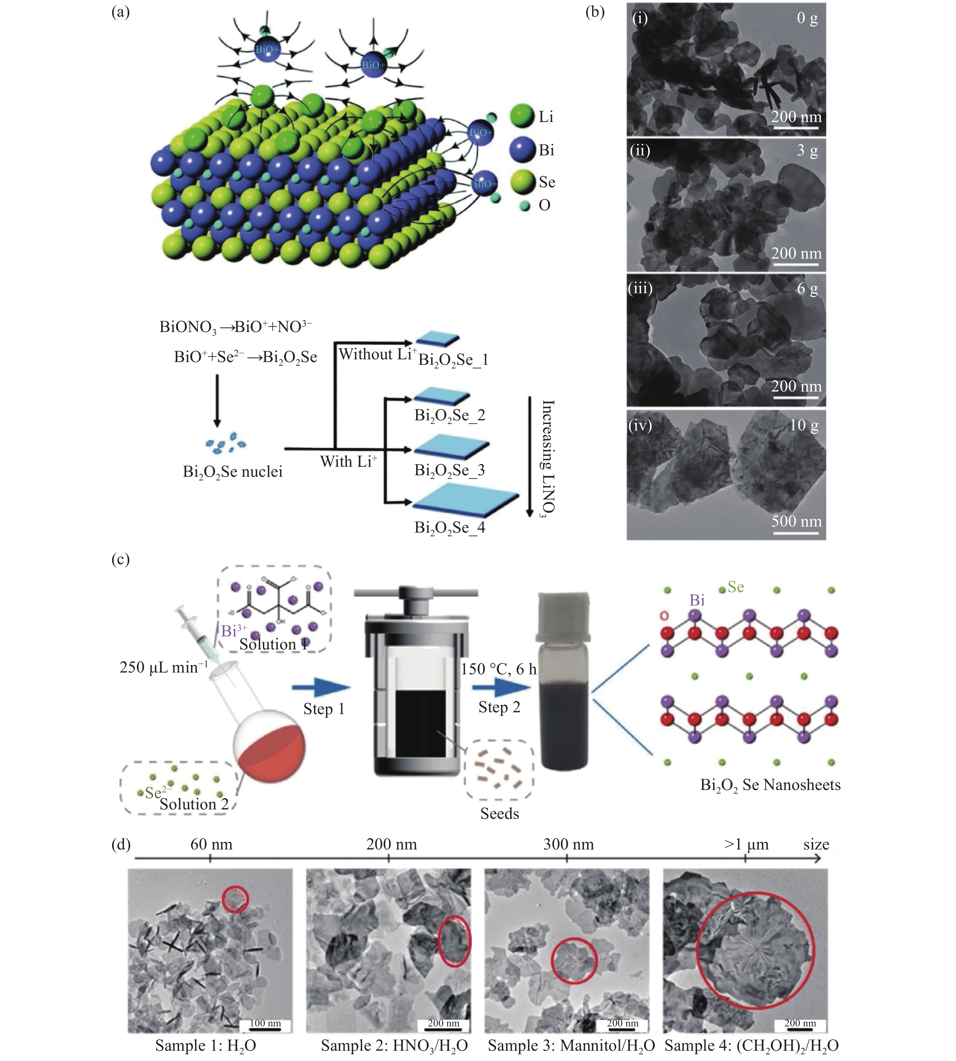
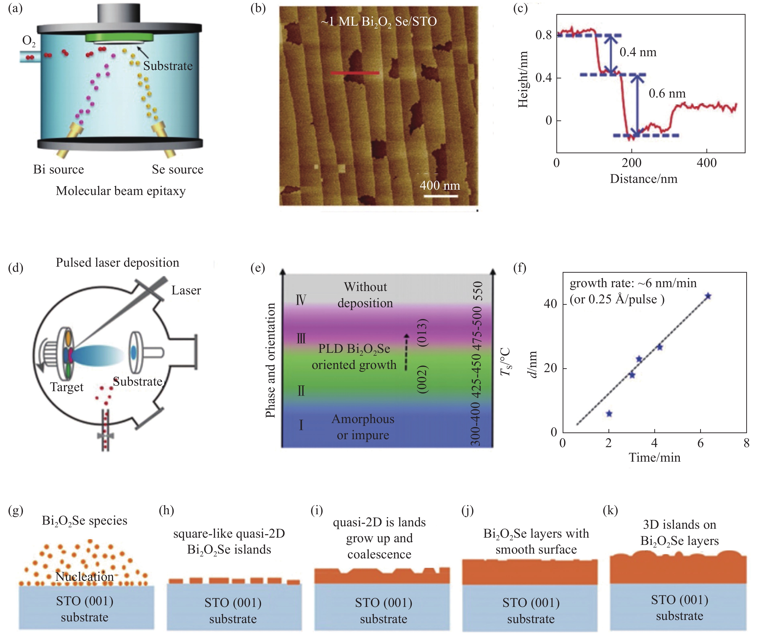
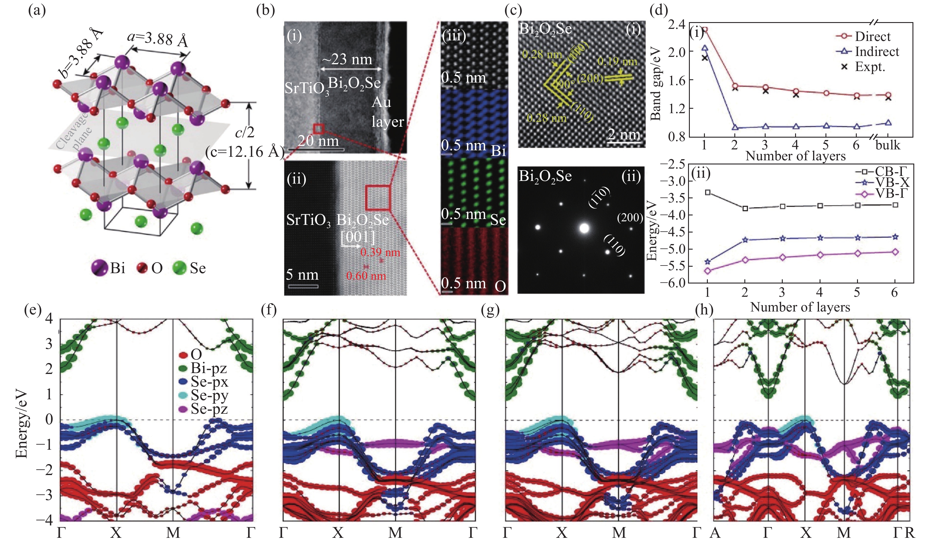
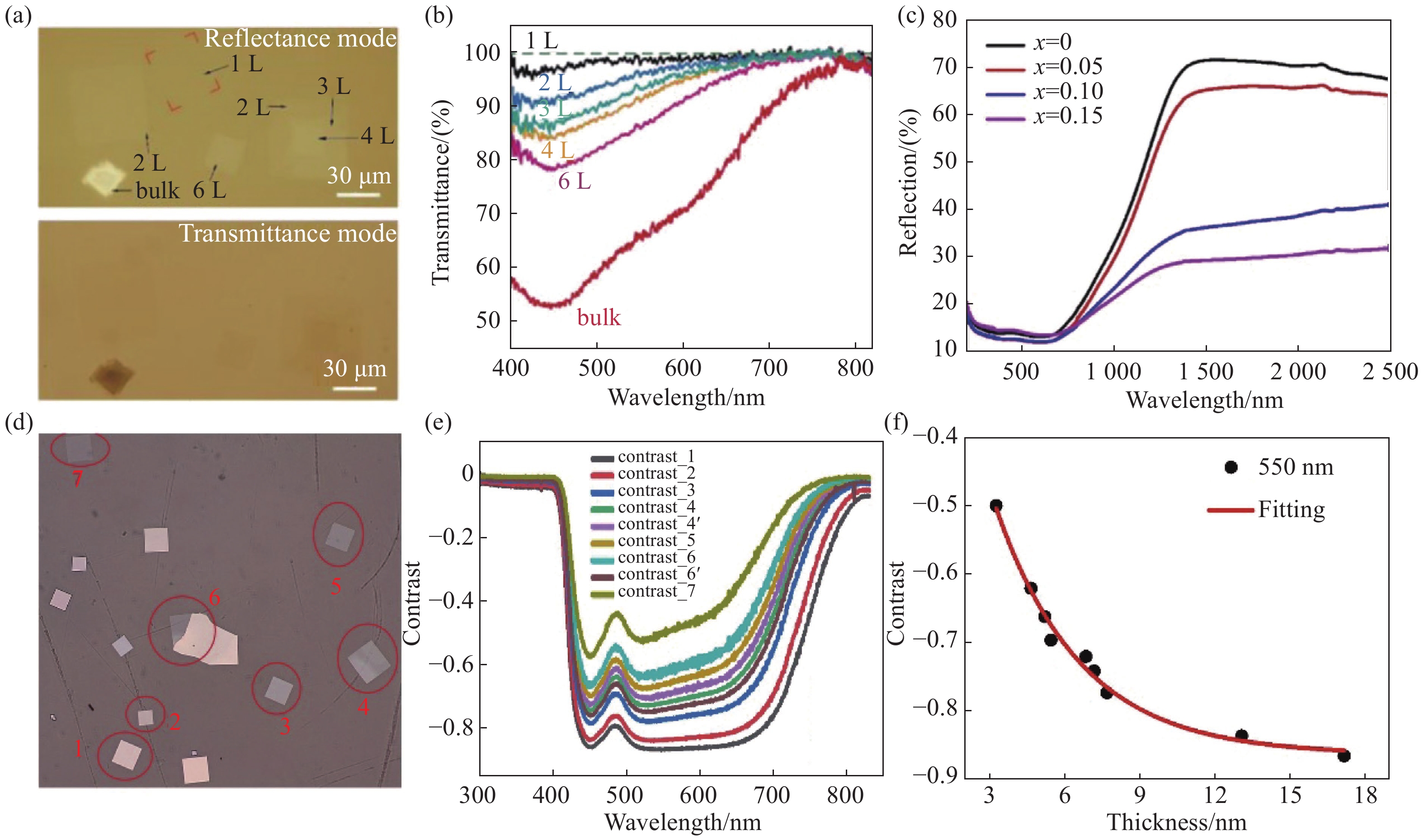
Two-dimensional (2D) Bi2O2Se has attracted broad attention in the field of electronic and optoelectronic applications in the UV-Vis-NIR region due to its unique crystal structure, energy band, high carrier mobility, and excellent stability. In this paper, we review the recent research progress in the material synthesis and optical characterization of Bi2O2Se. Firstly, the synthetic method and growth mechanism of 2D Bi2O2Se are introduced, including Chemical Vapor Deposition (CVD), wet chemical process, Molecular Beam Epitaxy (MBE) and Pulsed Laser Deposition (PLD), etc. Via steady-state spectrum study, the properties change of 2D Bi2O2Se with thickness change can be studied, such as the band gap. The defect type, temperature coefficient and thermal conductivity of 2D Bi2O2Se material can be further studied by focusing on the crystal vibration mode. Transient spectrum techniques can benefit the study of relaxation process and carriers transport properties in 2D Bi2O2Se materials. Finally, we summarize the existing challenges and application prospects for the promising Bi2O2Se field.

| [1] |
BUTLER S Z, HOLLEN S M, CAO L Y, et al. Progress, challenges, and opportunities in two-dimensional materials beyond graphene[J]. ACS Nano, 2013, 7(4): 2898-2926. doi: 10.1021/nn400280c
|
| [2] |
梁铮, 葛广路, 栾燕, 等. GB/T 30544.13-2018《纳米科技 术语 第13部分: 石墨烯及相关二维材料》核心术语介绍及解读[J]. 中国标准化,2019(S1):23-28.
LIANG ZH, GE G L, LUAN Y, et al. Introduction and interpretation of core vocabularies of GB/T 30544.13-2018, nanotechnologies-vocabulary-Part 13: graphene and related two-dimensional (2D) materials[J]. Standardization in China, 2019(S1): 23-28. (in Chinese)
|
| [3] |
LIU Y W, XIAO CH, LI ZH, et al. Vacancy engineering for tuning electron and phonon structures of two-dimensional materials[J]. Advanced Energy Materials, 2016, 6(23): 1600436. doi: 10.1002/aenm.201600436
|
| [4] |
GUPTA A, SAKTHIVEL T, SEAL S. Recent development in 2D materials beyond graphene[J]. Progress in Materials Science, 2015, 73: 44-126. doi: 10.1016/j.pmatsci.2015.02.002
|
| [5] |
张金月, 吕俊鹏, 倪振华. 二维材料异质结高灵敏度红外探测器[J]. 中国光学,2021,14(1):87-99. doi: 10.37188/CO.2020-0139
ZHANG J Y, LV J P, NI ZH H. Highly sensitive infrared detector based on a two-dimensional heterojunction[J]. Chinese Optics, 2021, 14(1): 87-99. (in Chinese) doi: 10.37188/CO.2020-0139
|
| [6] |
NOVOSELOV K S, GEIM A K, MOROZOV S V, et al. Electric field effect in atomically thin carbon films[J]. Science, 2004, 306(5696): 666-669. doi: 10.1126/science.1102896
|
| [7] |
MAK K F, LEE C, HONE J, et al. Atomically thin MoS2: a new direct-gap semiconductor[J]. Physical Review Letters, 2010, 105(13): 136805. doi: 10.1103/PhysRevLett.105.136805
|
| [8] |
AYARI A, COBAS E, OGUNDADEGBE O, et al. Realization and electrical characterization of ultrathin crystals of layered transition-metal dichalcogenides[J]. Journal of Applied Physics, 2007, 101(1): 014507. doi: 10.1063/1.2407388
|
| [9] |
LI L K, YU Y J, YE G J, et al. Black phosphorus field-effect transistors[J]. Nature Nanotechnology, 2014, 9(5): 372-377. doi: 10.1038/nnano.2014.35
|
| [10] |
MENG L, WANG Y L, ZHANG L ZH, et al. Buckled silicene formation on Ir(111)[J]. Nano Letters, 2013, 13(2): 685-690. doi: 10.1021/nl304347w
|
| [11] |
ZHU P CH, ZHU J. Low-dimensional metal halide perovskites and related optoelectronic applications[J]. InfoMat, 2020, 2(2): 341-378. doi: 10.1002/inf2.12086
|
| [12] |
NAGUIB M, KURTOGLU M, PRESSER V, et al. Two-dimensional nanocrystals produced by exfoliation of Ti3AlC2[J]. Advanced Materials, 2011, 23(37): 4248-4253. doi: 10.1002/adma.201102306
|
| [13] |
HONG Y L, LIU ZH B, WANG L, et al. Chemical vapor deposition of layered two-dimensional MoSi2N4 materials[J]. Science, 2020, 369(6504): 670-674. doi: 10.1126/science.abb7023
|
| [14] |
HUO N J, KONSTANTATOS G. Recent progress and future prospects of 2D-based photodetectors[J]. Advanced Materials, 2018, 30(51): 1801164. doi: 10.1002/adma.201801164
|
| [15] |
JING X, ILLARIONOV Y, YALON E, et al. Engineering field effect transistors with 2D semiconducting channels: Status and prospects[J]. Advanced Functional Materials, 2020, 30(18): 1901971. doi: 10.1002/adfm.201901971
|
| [16] |
SANGWAN V K, HERSAM M C. Neuromorphic nanoelectronic materials[J]. Nature Nanotechnology, 2020, 15(7): 517-528. doi: 10.1038/s41565-020-0647-z
|
| [17] |
SHIFA T A, WANG F M, LIU Y, et al. Heterostructures based on 2D materials: A versatile platform for efficient catalysis[J]. Advanced Materials, 2019, 31(45): 1804828. doi: 10.1002/adma.201804828
|
| [18] |
ZHANG X Y, HOU L L, CIESIELSKI A, et al. 2D materials beyond graphene for high-performance energy storage applications[J]. Advanced Energy Materials, 2016, 6(23): 1600671. doi: 10.1002/aenm.201600671
|
| [19] |
ZHANG Y B, TANG T T, GIRIT C, et al. Direct observation of a widely tunable bandgap in bilayer graphene[J]. Nature, 2009, 459(7248): 820-823. doi: 10.1038/nature08105
|
| [20] |
SCHWIERZ F. Graphene transistors[J]. Nature Nanotechnology, 2010, 5(7): 487-496. doi: 10.1038/nnano.2010.89
|
| [21] |
JARIWALA D, SANGWAN V K, LAUHON L J, et al. Emerging device applications for semiconducting two-dimensional transition metal dichalcogenides[J]. ACS Nano, 2014, 8(2): 1102-1120. doi: 10.1021/nn500064s
|
| [22] |
CUI X, LEE G H, KIM Y D, et al. Multi-terminal transport measurements of MoS2 using a van der Waals heterostructure device platform[J]. Nature Nanotechnology, 2015, 10(6): 534-540. doi: 10.1038/nnano.2015.70
|
| [23] |
ZHANG SH, YANG J, XU R J, et al. Extraordinary photoluminescence and strong temperature/angle-dependent Raman responses in few-layer phosphorene[J]. ACS Nano, 2014, 8(9): 9590-9596. doi: 10.1021/nn503893j
|
| [24] |
ISLAND J O, STEELE G A, VAN DER ZANT H S, et al. Environmental instability of few-layer black phosphorus[J]. 2D Materials, 2015, 2(1): 011002. doi: 10.1088/2053-1583/2/1/011002
|
| [25] |
CHEN CH, WANG M X, WU J X, et al. Electronic structures and unusually robust bandgap in an ultrahigh-mobility layered oxide semiconductor, Bi2O2Se[J]. Science Advances, 2018, 4(9): eaat8355. doi: 10.1126/sciadv.aat8355
|
| [26] |
WU J X, YUAN H T, MENG M M, et al. High electron mobility and quantum oscillations in non-encapsulated ultrathin semiconducting Bi2O2Se[J]. Nature Nanotechnology, 2017, 12(6): 530-534. doi: 10.1038/nnano.2017.43
|
| [27] |
TIAN X L, LUO H Y, WEI R F, et al. An ultrabroadband Mid-infrared pulsed optical switch employing solution-processed bismuth oxyselenide[J]. Advanced Materials, 2018, 30(31): 1801021. doi: 10.1002/adma.201801021
|
| [28] |
SONG CH CH, SONG Y L, PAN L, et al. Thermoelectric properties of Bi2-xTixO2Se with the shear exfoliation-restacking process[J]. Journal of Alloys and Compounds, 2022, 892: 162147. doi: 10.1016/j.jallcom.2021.162147
|
| [29] |
ZHANG Z Y, LI T R, WU Y J, et al. Truly concomitant and independently expressed short-and long-term plasticity in a Bi2O2Se-based three-terminal memristor[J]. Advanced Materials, 2019, 31(3): 1805769. doi: 10.1002/adma.201805769
|
| [30] |
YANG C M, CHEN T C, VERMA D, et al. Bidirectional all-optical synapses based on a 2D Bi2O2Se/Graphene hybrid structure for multifunctional optoelectronics[J]. Advanced Functional Materials, 2020, 30(30): 2001598. doi: 10.1002/adfm.202001598
|
| [31] |
WU J X, TAN C W, TAN ZH J, et al. Controlled synthesis of high-mobility atomically thin bismuth oxyselenide crystals[J]. Nano Letters, 2017, 17(5): 3021-3026. doi: 10.1021/acs.nanolett.7b00335
|
| [32] |
HOSSAIN M T, GIRI P K. Temperature-dependent Raman studies and thermal conductivity of direct CVD grown non-van der Waals layered Bi2O2Se[J]. Journal of Applied Physics, 2021, 129(17): 175102. doi: 10.1063/5.0049368
|
| [33] |
YANG X, ZHANG Q, SONG Y CH, et al. High mobility two-dimensional bismuth oxyselenide single crystals with large grain size grown by reverse-flow chemical vapor deposition[J]. ACS Applied Materials &Interfaces, 2021, 13(41): 49153-49162.
|
| [34] |
SUN Y, YE S, ZHANG J, et al. Lithium nitrate-assisted hydrothermal synthesis of ultrathin Bi2O2Se nanosheets and their photoelectrochemical performance[J]. Journal of Materials Chemistry C, 2020, 8(42): 14711-14717. doi: 10.1039/D0TC04352D
|
| [35] |
PANG X X, ZHAO Y T, GAO X X, et al. Two-step colloidal synthesis of micron-scale Bi2O2Se nanosheets and their electrostatic assembly for thin-film photodetectors with fast response[J]. Chinese Chemical Letters, 2021, 32(10): 3099-3104. doi: 10.1016/j.cclet.2021.03.039
|
| [36] |
ZHANG K Y, HU CH G, KANG X L, et al. Synthesis and thermoelectric properties of Bi2O2Se nanosheets[J]. Materials Research Bulletin, 2013, 48(10): 3968-3972. doi: 10.1016/j.materresbull.2013.06.013
|
| [37] |
LIANG Y, CHEN Y J, SUN Y W, et al. Molecular beam epitaxy and electronic structure of atomically thin oxyselenide films[J]. Advanced Materials, 2019, 31(39): 1901964. doi: 10.1002/adma.201901964
|
| [38] |
SONG Y K, LI ZH J, LI H, et al. Epitaxial growth and characterization of high quality Bi2O2Se thin films on SrTiO3 substrates by pulsed laser deposition[J]. Nanotechnology, 2020, 31(16): 165704. doi: 10.1088/1361-6528/ab6686
|
| [39] |
HU C W, YANG Y, HOU CH J, et al. Thickness-and strain-tunable electronic structures of two-dimensional Bi2O2Se[J]. Computational Materials Science, 2021, 194: 110424. doi: 10.1016/j.commatsci.2021.110424
|
| [40] |
NI Z H, WANG H M, KASIM J, et al. Graphene thickness determination using reflection and contrast spectroscopy[J]. Nano Letters, 2007, 7(9): 2758-2763. doi: 10.1021/nl071254m
|
| [41] |
KIM U J, NAM S H, SEO J, et al. Visualizing line defects in non-van der Waals Bi2O2Se using raman spectroscopy[J]. ACS Nano, 2022, 16(3): 3637-3646. doi: 10.1021/acsnano.1c06598
|
| [42] |
CHENG T, TAN C W, ZHANG SH Q, et al. Raman spectra and strain effects in bismuth oxychalcogenides[J]. The Journal of Physical Chemistry C, 2018, 122(34): 19970-19980. doi: 10.1021/acs.jpcc.8b05475
|
| [43] |
YANG F, WANG R D, ZHAO W W, et al. Thermal transport and energy dissipation in two-dimensional Bi2O2Se[J]. Applied Physics Letters, 2019, 115(19): 193103. doi: 10.1063/1.5123682
|
| [44] |
HAN Y D, LIU Y G, GU CH, et al. Ultrafast carrier dynamics of Bi2O2Se nanoplates in the nonlinear excitation regime[J]. Chemical Physics, 2021, 541: 111017. doi: 10.1016/j.chemphys.2020.111017
|
| [45] |
LIU SH Y, TAN C W, HE D W, et al. Optical properties and photocarrier dynamics of Bi2O2Se monolayer and nanoplates[J]. Advanced Optical Materials, 2020, 8(6): 1901567. doi: 10.1002/adom.201901567
|
| [46] |
BOLLER H. Die kristallstruktur von Bi2O2Se[J]. Monatshefte für Chemie/Chemical Monthly, 1973, 104(4): 916-919.
|
| [47] |
RULEOVA P, DRASAR C, LOSTAK P, et al. Thermoelectric properties of Bi2O2Se[J]. Materials Chemistry and Physics, 2010, 119(1-2): 299-302. doi: 10.1016/j.matchemphys.2009.08.067
|
| [48] |
DRASAR C, RULEOVA P, BENES L, et al. Preparation and transport properties of Bi2O2Se single crystals[J]. Journal of Electronic Materials, 2012, 41(9): 2317-2321. doi: 10.1007/s11664-012-2143-1
|
| [49] |
PAN L, ZHAO L, ZHANG X X, et al. Significant optimization of electron–phonon transport of n-Type Bi2O2Se by mechanical manipulation of Se vacancies via shear exfoliation[J]. ACS Applied Materials &Interfaces, 2019, 11(24): 21603-21609.
|
| [50] |
ZHAN B, LIU Y CH, TAN X, et al. Enhanced thermoelectric properties of Bi2O2Se ceramics by Bi deficiencies[J]. Journal of the American Ceramic Society, 2015, 98(8): 2465-2469. doi: 10.1111/jace.13619
|
| [51] |
TAN X, LIU Y CH, LIU R, et al. Synergistical enhancement of thermoelectric properties in n-Type Bi2O2Se by carrier engineering and hierarchical microstructure[J]. Advanced Energy Materials, 2019, 9(31): 1900354. doi: 10.1002/aenm.201900354
|
| [52] |
ZHAN B, BUTT S, LIU Y CH, et al. High-temperature thermoelectric behaviors of Sn-doped n-type Bi2O2Se ceramics[J]. Journal of Electroceramics, 2015, 34(2): 175-179.
|
| [53] |
ZHAN B, LIU Y CH, LAN J L, et al. Enhanced thermoelectric performance of Bi2O2Se with Ag addition[J]. Materials, 2015, 8(4): 1568-1576. doi: 10.3390/ma8041568
|
| [54] |
YIN J B, TAN ZH J, HONG H, et al. Ultrafast and highly sensitive infrared photodetectors based on two-dimensional oxyselenide crystals[J]. Nature Communications, 2018, 9: 3311. doi: 10.1038/s41467-018-05874-2
|
| [55] |
LI J, WANG ZH X, WEN Y, et al. High-performance near-infrared photodetector based on ultrathin Bi2O2Se nanosheets[J]. Advanced Functional Materials, 2018, 28(10): 1706437. doi: 10.1002/adfm.201706437
|
| [56] |
WEI Q L, LI R P, LIN CH Q, et al. Quasi-two-dimensional se-terminated bismuth oxychalcogenide (Bi2O2Se)[J]. ACS Nano, 2019, 13(11): 13439-13444. doi: 10.1021/acsnano.9b07000
|
| [57] |
MENG M M, HUANG SH Y, TAN C W, et al. Universal conductance fluctuations and phase-coherent transport in a semiconductor Bi2O2Se nanoplate with strong spin–orbit interaction[J]. Nanoscale, 2019, 11(22): 10622-10628. doi: 10.1039/C9NR02347J
|
| [58] |
FU H X, WU J X, PENG H L, et al. Self-modulation doping effect in the high-mobility layered semiconductor Bi2O2Se[J]. Physical Review B, 2018, 97(24): 241203. doi: 10.1103/PhysRevB.97.241203
|
| [59] |
TONG T, LI W SH, QIN SH CH, et al. Bi2O2Se/Au-based schottky phototransistor with fast response and ultrahigh responsivity[J]. IEEE Electron Device Letters, 2020, 41(10): 1464-1467. doi: 10.1109/LED.2020.3016186
|
| [60] |
LUO P, ZHUGE F W, WANG F K, et al. PbSe quantum dots sensitized high-mobility Bi2O2Se nanosheets for high-performance and broadband photodetection beyond 2 μm[J]. ACS Nano, 2019, 13(8): 9028-9037. doi: 10.1021/acsnano.9b03124
|
| [61] |
WU J X, LIU Y J, TAN ZH J, et al. Chemical patterning of high-mobility semiconducting 2D Bi2O2Se crystals for integrated optoelectronic Devices[J]. Advanced Materials, 2017, 29(44): 1704060. doi: 10.1002/adma.201704060
|
| [62] |
WU J X, QIU CH G, FU H X, et al. Low residual carrier concentration and high mobility in 2D semiconducting Bi2O2Se[J]. Nano Letters, 2018, 19(1): 197-202.
|
| [63] |
YING J H, HE J B, YANG G, et al. Magnitude and spatial distribution control of the supercurrent in Bi2O2Se-based josephson junction[J]. Nano Letters, 2020, 20(4): 2569-2575. doi: 10.1021/acs.nanolett.0c00025
|
| [64] |
FU Q D, ZHU CH, ZHAO X X, et al. Ultrasensitive 2D Bi2O2Se phototransistors on silicon substrates[J]. Advanced Materials, 2019, 31(1): 1804945. doi: 10.1002/adma.201804945
|
| [65] |
TAN C W, TANG M, WU J X, et al. Wafer-scale growth of single-crystal 2D semiconductor on perovskite oxides for high-performance transistors[J]. Nano Letters, 2019, 19(3): 2148-2153. doi: 10.1021/acs.nanolett.9b00381
|
| [66] |
WU ZH, LIU G L, WANG Y X, et al. Seed‐induced vertical growth of 2D Bi2O2Se nanoplates by chemical vapor transport[J]. Advanced Functional Materials, 2019, 29(50): 1906639. doi: 10.1002/adfm.201906639
|
| [67] |
KANG M, CHAI H J, JEONG H B, et al. Low-temperature and high-quality growth of Bi2O2Se layered semiconductors via cracking metal–organic chemical vapor deposition[J]. ACS Nano, 2021, 15(5): 8715-8723. doi: 10.1021/acsnano.1c00811
|
| [68] |
KHAN U, LUO Y T, TANG L, et al. Controlled vapor–solid deposition of millimeter‐size single crystal 2D Bi2O2Se for high‐performance phototransistors[J]. Advanced Functional Materials, 2019, 29(14): 1807979. doi: 10.1002/adfm.201807979
|
| [69] |
XIONG J Y, CHENG G, LU ZH, et al. BiOCOOH hierarchical nanostructures: Shape-controlled solvothermal synthesis and photocatalytic degradation performances[J]. CrystEngComm, 2011, 13(7): 2381-2390. doi: 10.1039/c0ce00705f
|
| [70] |
LI Y Y, WANG G, ZHU X G, et al. Intrinsic topological insulator Bi2Te3 thin films on Si and their thickness limit[J]. Advanced Materials, 2010, 22(36): 4002-4007. doi: 10.1002/adma.201000368
|
| [71] |
STOUGHTON S, SHOWAK M, MAO Q, et al. Adsorption-controlled growth of BiVO4 by molecular-beam epitaxy[J]. APL Materials, 2013, 1(4): 042112. doi: 10.1063/1.4824041
|
| [72] |
LI T R, TU T, SUN Y W, et al. A native oxide high-κ gate dielectric for two-dimensional electronics[J]. Nature Electronics, 2020, 3(8): 473-478. doi: 10.1038/s41928-020-0444-6
|
| [73] |
LI T R, PENG H L. 2D Bi2O2Se: an emerging material platform for the next-generation electronic industry[J]. Accounts of Materials Research, 2021, 2(9): 842-853. doi: 10.1021/accountsmr.1c00130
|
| [74] |
LIANG Y, ZHOU X H, LI W, et al. Preparation of two-dimensional [Bi2O2]-based layered materials: Progress and prospects[J]. APL Materials, 2021, 9(6): 060905. doi: 10.1063/5.0052300
|
| [75] |
TONG T, ZHANG M H, CHEN Y Q, et al. Ultrahigh Hall mobility and suppressed backward scattering in layered semiconductor Bi2O2Se[J]. Applied Physics Letters, 2018, 113(7): 072106. doi: 10.1063/1.5042727
|
| [76] |
MAO Q H, GENG X D, YANG J F, et al. Synthesis and electrical transport properties of Bi2O2Se single crystals[J]. Journal of Crystal Growth, 2018, 498: 244-247. doi: 10.1016/j.jcrysgro.2018.07.004
|
| [77] |
YANG S J, LUO P, WANG F K, et al. Van der waals epitaxy of Bi2Te2Se/Bi2O2Se vertical heterojunction for high performance photodetector[J]. Small, 2022, 18(6): 2105211. doi: 10.1002/smll.202105211
|
| [78] |
LIDE D R. CRC Handbook of Chemistry and Physics[M]. 86th ed. Boca Raton, FL: CRC Press, 2005, 4: 128-129.
|
| [79] |
HORÁK J, STARY Z, LOŠŤÁK P, et al. Anti-site defects in n-Bi2Se3 crystals[J]. Journal of Physics and Chemistry of Solids, 1990, 51(12): 1353-1360. doi: 10.1016/0022-3697(90)90017-A
|
| [80] |
LIU D, GUO Y ZH, FANG L, et al. Sulfur vacancies in monolayer MoS2 and its electrical contacts[J]. Applied Physics Letters, 2013, 103(18): 183113. doi: 10.1063/1.4824893
|
| [81] |
PADILHA J E, PEELAERS H, JANOTTI A, et al. Nature and evolution of the band-edge states in MoS2: From monolayer to bulk[J]. Physical Review B, 2014, 90(20): 205420. doi: 10.1103/PhysRevB.90.205420
|
| [82] |
TRAN V, FEI R X, YANG L. Quasiparticle energies, excitons, and optical spectra of few-layer black phosphorus[J]. 2D Materials, 2015, 2(4): 044014. doi: 10.1088/2053-1583/2/4/044014
|
| [83] |
ZHU X L, LIU P F, XIE G F, et al. First-principles study of thermal transport properties in the two-and three-dimensional forms of Bi2O2Se[J]. Physical Chemistry Chemical Physics, 2019, 21(21): 10931-10938. doi: 10.1039/C9CP01867K
|
| [84] |
YU J B, SUN Q. Bi2O2Se nanosheet: An excellent high-temperature n-type thermoelectric material[J]. Applied Physics Letters, 2018, 112(5): 053901. doi: 10.1063/1.5017217
|
| [85] |
HONG H Y, KIM D H, WON S O, et al. Enhancement of the thermoelectric performance of n- type Bi2O2Se by Ce4+ doping[J]. Journal of Materials Research and Technology, 2021, 15: 4161-4172. doi: 10.1016/j.jmrt.2021.10.002
|
| [86] |
XIE B, YANG F, AN X H, et al. . Controlled growth and optical characterization of high mobility layered semiconductor Bi2O2Se. (unpublished)
|
| [87] |
张雁, 尹利辉, 冯芳. 拉曼光谱分析法的应用介绍[J]. 药物分析杂志,2009,29(7):1236-1241. doi: 10.16155/j.0254-1793.2009.07.001
ZHANG Y, YIN L H, FENG F. Introduction for the application of Raman scattering method[J]. Chinese Journal of Pharmaceutical Analysis, 2009, 29(7): 1236-1241. (in Chinese) doi: 10.16155/j.0254-1793.2009.07.001
|
| [88] |
侯翔宇, 邱腾. 低维光电材料缺陷与界面增强拉曼散射[J]. 中国光学,2021,14(1):170-181. doi: 10.37188/CO.2020-0145
HOU X Y, QIU T. Defects- and interface-enhanced Raman scattering in low-dimensional optoelectronic materials[J]. Chinese Optics, 2021, 14(1): 170-181. (in Chinese) doi: 10.37188/CO.2020-0145
|
| [89] |
PEREIRA A L J, SANTAMARÍA-PÉREZ D, RUIZ-FUERTES J, et al. Experimental and theoretical Study of Bi2O2Se under compression[J]. The Journal of Physical Chemistry C, 2018, 122(16): 8853-8867. doi: 10.1021/acs.jpcc.8b02194
|
| [90] |
CHEN SH Y, ZHENG CH X, FUHRER M S, et al. Helicity-resolved Raman scattering of MoS2, MoSe2, WS2, and WSe2 atomic layers[J]. Nano Letters, 2015, 15(4): 2526-2532. doi: 10.1021/acs.nanolett.5b00092
|
| [91] |
TAN Q H, SUN Y J, LIU X L, et al. Observation of forbidden phonons, Fano resonance and dark excitons by resonance Raman scattering in few-layer WS2[J]. 2D Materials, 2017, 4(3): 031007. doi: 10.1088/2053-1583/aa79bb
|
| [92] |
KIM S, KIM K, LEE J U, et al. Excitonic resonance effects and Davydov splitting in circularly polarized Raman spectra of few-layer WSe2[J]. 2D Materials, 2017, 4(4): 045002. doi: 10.1088/2053-1583/aa8312
|
| [93] |
LEE J U, WOO S, PARK J, et al. Strain-shear coupling in bilayer MoS2[J]. Nature Communications, 2017, 8(1): 1370. doi: 10.1038/s41467-017-01487-3
|
| [94] |
KIM J, LEE J U, LEE J, et al. Anomalous polarization dependence of Raman scattering and crystallographic orientation of black phosphorus[J]. Nanoscale, 2015, 7(44): 18708-18715. doi: 10.1039/C5NR04349B
|
| [95] |
HUANG M Y, YAN H G, CHEN CH Y, et al. Phonon softening and crystallographic orientation of strained graphene studied by Raman spectroscopy[J]. Proceedings of the National Academy of Sciences of the United States of America, 2009, 106(18): 7304-7308. doi: 10.1073/pnas.0811754106
|
| [96] |
WANG Y L, CONG CH X, QIU C Y, et al. Raman spectroscopy study of lattice vibration and crystallographic orientation of monolayer MoS2 under uniaxial strain[J]. Small, 2013, 9(17): 2857-2861. doi: 10.1002/smll.201202876
|
| [97] |
CONLEY H J, WANG B, ZIEGLER J I, et al. Bandgap engineering of strained monolayer and bilayer MoS2[J]. Nano Letters, 2013, 13(8): 3626-3630. doi: 10.1021/nl4014748
|
| [98] |
RIBEIRO-SOARES J, ALMEIDA R M, BARROS E B, et al. Group theory analysis of phonons in two-dimensional transition metal dichalcogenides[J]. Physical Review B, 2014, 90(11): 115438. doi: 10.1103/PhysRevB.90.115438
|
| [99] |
YOU Y M, NI ZH H, YU T, et al. Edge chirality determination of graphene by Raman spectroscopy[J]. Applied Physics Letters, 2008, 93(16): 163112. doi: 10.1063/1.3005599
|
| [100] |
LEE U, HAN Y, LEE S, et al. Time evolution studies on strain and doping of graphene grown on a copper substrate using Raman spectroscopy[J]. ACS Nano, 2020, 14(1): 919-926. doi: 10.1021/acsnano.9b08205
|
| [101] |
SAHOO S, MALLIK S K, SAHU M C, et al. Thermal conductivity of free-standing silicon nanowire using Raman spectroscopy[J]. Nanotechnology, 2020, 31(50): 505701. doi: 10.1088/1361-6528/abb42c
|
| [102] |
SAHOO S, GAUR A P S, AHMADI M, et al. Temperature-dependent Raman studies and thermal conductivity of few-layer MoS2[J]. The Journal of Physical Chemistry C, 2013, 117(17): 9042-9047. doi: 10.1021/jp402509w
|
| [103] |
ZHANG X, SUN D ZH, LI Y L, et al. Measurement of lateral and interfacial thermal conductivity of single-and bilayer MoS2 and MoSe2 using refined optothermal Raman technique[J]. ACS Applied Materials &Interfaces, 2015, 7(46): 25923-25929.
|
| [104] |
PEIMYOO N, SHANG J ZH, YANG W H, et al. Thermal conductivity determination of suspended mono-and bilayer WS2 by Raman spectroscopy[J]. Nano Research, 2015, 8(4): 1210-1221. doi: 10.1007/s12274-014-0602-0
|
| [105] |
LANZILLO N A, BIRDWELL A G, AMANI M, et al. Temperature-dependent phonon shifts in monolayer MoS2[J]. Applied Physics Letters, 2013, 103(9): 093102. doi: 10.1063/1.4819337
|
| [106] |
BALKANSKI M, WALLIS R F, HARO E. Anharmonic effects in light scattering due to optical phonons in silicon[J]. Physical Review B, 1983, 28(4): 1928-1934. doi: 10.1103/PhysRevB.28.1928
|
| [107] |
NILSSON G, NELIN G. Phonon dispersion relations in Ge at 80 K[J]. Physical Review B, 1971, 3(2): 364-369. doi: 10.1103/PhysRevB.3.364
|
| [108] |
BALANDIN A A, GHOSH S, BAO W ZH, et al. Superior thermal conductivity of single-layer graphene[J]. Nano Letters, 2008, 8(3): 902-907. doi: 10.1021/nl0731872
|
| [109] |
LUO Z, MAASSEN J, DENG Y X, et al. Anisotropic in-plane thermal conductivity observed in few-layer black phosphorus[J]. Nature Communications, 2015, 6(1): 8572. doi: 10.1038/ncomms9572
|
| [110] |
HUANG L B, HARTLAND G V, CHU L Q, et al. Ultrafast transient absorption microscopy studies of carrier dynamics in epitaxial graphene[J]. Nano Letters, 2010, 10(4): 1308-1313. doi: 10.1021/nl904106t
|
| [111] |
YU J H, SHARMA M, SHARMA A, et al. All-optical control of exciton flow in a colloidal quantum well complex[J]. Light:Science &Applications, 2020, 9: 27.
|
| [112] |
YU J H, HOU S Y, SHARMA M, et al. Strong plasmon-wannier mott exciton interaction with high aspect ratio colloidal quantum wells[J]. Matter, 2020, 2(6): 1550-1563. doi: 10.1016/j.matt.2020.03.013
|
| [113] |
YU J H, SHENDRE S, KOH W K, et al. Electrically control amplified spontaneous emission in colloidal quantum dots[J]. Science Advances, 2019, 5(10): eaav3140. doi: 10.1126/sciadv.aav3140
|
| [114] |
王云坤, 李耀龙, 高宇南. 二维过渡金属硫族化合物中的缺陷和相关载流子动力学的研究进展[J]. 中国光学,2021,14(1):18-42. doi: 10.37188/CO.2020-0106
WANG Y K, LI Y L, GAO Y N. Progress on defect and related carrier dynamics in two-dimensional transition metal chalcogenides[J]. Chinese Optics, 2021, 14(1): 18-42. (in Chinese) doi: 10.37188/CO.2020-0106
|
| [115] |
SUNDARAM S K, MAZUR E. Inducing and probing non-thermal transitions in semiconductors using femtosecond laser pulses[J]. Nature Materials, 2002, 1(4): 217-224. doi: 10.1038/nmat767
|
| [116] |
SCHÄFER S, LIANG W X, ZEWAIL A H. Primary structural dynamics in graphite[J]. New Journal of Physics, 2011, 13(6): 063030. doi: 10.1088/1367-2630/13/6/063030
|
| [117] |
RUZICKA B A, WERAKE L K, SAMASSEKOU H, et al. Ambipolar diffusion of photoexcited carriers in bulk GaAs[J]. Applied Physics Letters, 2010, 97(26): 262119. doi: 10.1063/1.3533664
|
| [118] |
KUMAR N, CUI Q N, CEBALLOS F, et al. Exciton-exciton annihilation in MoSe2 monolayers[J]. Physical Review B, 2014, 89(12): 125427. doi: 10.1103/PhysRevB.89.125427
|
| [119] |
SUN D ZH, RAO Y, REIDER G A, et al. Observation of rapid exciton–exciton annihilation in monolayer molybdenum disulfide[J]. Nano Letters, 2014, 14(10): 5625-5629. doi: 10.1021/nl5021975
|
| [120] |
YUAN L, HUANG L B. Exciton dynamics and annihilation in WS2 2D semiconductors[J]. Nanoscale, 2015, 7(16): 7402-7408. doi: 10.1039/C5NR00383K
|
Figures(9)


 DownLoad: