| Citation: | LI Hao, HU De-jiao, QIN Fei, LI Xiang-ping. Principle and application of metasurface optical field modulation of atomic layer thickness[J]. Chinese Optics, 2021, 14(4): 851-866. doi: 10.37188/CO.2021-0069

|

| [1] |
ENKRICH C, WEGENER M, LINDEN S, et al. Magnetic metamaterials at telecommunication and visible frequencies[J]. Physical Review Letters, 2005, 95(20): 203901. doi: 10.1103/PhysRevLett.95.203901
|
| [2] |
VALENTINE J, ZHANG SH, ZENTGRAF T, et al. Three-dimensional optical metamaterial with a negative refractive index[J]. Nature, 2008, 455(7211): 376-379. doi: 10.1038/nature07247
|
| [3] |
WANG L Y, SMITH K W, DOMINGUEZ-MEDINA S, et al. Circular differential scattering of single chiral self-assembled gold nanorod dimers[J]. ACS Photonics, 2015, 2(11): 1602-1610. doi: 10.1021/acsphotonics.5b00395
|
| [4] |
YU N F, GENEVET P, AIETA F, et al. Flat optics: controlling wavefronts with optical antenna metasurfaces[J]. IEEE Journal of Selected Topics in Quantum Electronics, 2013, 19(3): 4700423. doi: 10.1109/JSTQE.2013.2241399
|
| [5] |
KUMAR K, DUAN H G, HEGDE R S, et al. Printing colour at the optical diffraction limit[J]. Nature Nanotechnology, 2012, 7(9): 557-561. doi: 10.1038/nnano.2012.128
|
| [6] |
NI X J, KILDISHEV A V, SHALAEV V M. Metasurface holograms for visible light[J]. Nature Communications, 2013, 4(1): 2807. doi: 10.1038/ncomms3807
|
| [7] |
CLAUSEN J S, HØJLUND-NIELSEN E, CHRISTIANSEN A B, et al. Plasmonic metasurfaces for coloration of plastic consumer products[J]. Nano Letters, 2014, 14(8): 4499-4504. doi: 10.1021/nl5014986
|
| [8] |
YU N F, GENEVET P, KATS M A, et al. Light propagation with phase discontinuities: generalized laws of reflection and refraction[J]. Science, 2011, 334(6054): 333-337. doi: 10.1126/science.1210713
|
| [9] |
YU N F, AIETA F, GENEVET P, et al. A broadband, background-free quarter-wave plate based on plasmonic metasurfaces[J]. Nano Letters, 2012, 12(12): 6328-6333. doi: 10.1021/nl303445u
|
| [10] |
CHEN W T, YANG K Y, WANG C M, et al. High-efficiency broadband meta-hologram with polarization-controlled dual images[J]. Nano Letters, 2014, 14(1): 225-230. doi: 10.1021/nl403811d
|
| [11] |
GAO L H, CHENG Q, YANG J, et al. Broadband diffusion of terahertz waves by multi-bit coding metasurfaces[J]. Light:Science &Applications, 2015, 4(9): e324.
|
| [12] |
MUELLER J P B, RUBIN N A, DEVLIN R C, et al. Metasurface polarization optics: independent phase control of arbitrary orthogonal states of polarization[J]. Physical Review Letters, 2017, 118(11): 113901. doi: 10.1103/PhysRevLett.118.113901
|
| [13] |
WEN D D, YUE F Y, LI G X, et al. Helicity multiplexed broadband metasurface holograms[J]. Nature Communications, 2015, 6: 8241. doi: 10.1038/ncomms9241
|
| [14] |
DENG Z L, JIN M K, YE X, et al. Full‐color complex‐amplitude vectorial holograms based on multi‐freedom metasurfaces[J]. Advanced Functional Materials, 2020, 30(21): 1910610. doi: 10.1002/adfm.201910610
|
| [15] |
LI X, CHEN L W, LI Y, et al. Multicolor 3D meta-holography by broadband plasmonic modulation[J]. Science Advances, 2016, 2(11): e1601102. doi: 10.1126/sciadv.1601102
|
| [16] |
SUN SH L, YANG K Y, WANG C M, et al. High-efficiency broadband anomalous reflection by gradient meta-surfaces[J]. Nano Letters, 2012, 12(12): 6223-6229. doi: 10.1021/nl3032668
|
| [17] |
ZHENG G X, MÜHLENBERND H, KENNEY M, et al. Metasurface holograms reaching 80% efficiency[J]. Nature Nanotechnology, 2015, 10(4): 308-312. doi: 10.1038/nnano.2015.2
|
| [18] |
DENG J, YANG Y, TAO J, et al. Spatial frequency multiplexed meta-holography and meta-nanoprinting[J]. ACS Nano, 2019, 13(8): 9237-9246. doi: 10.1021/acsnano.9b03738
|
| [19] |
AIETA F, GENEVET P, KATS M A, et al. Aberration-free ultrathin flat lenses and axicons at telecom wavelengths based on plasmonic metasurfaces[J]. Nano Letters, 2012, 12(9): 4932-4936. doi: 10.1021/nl302516v
|
| [20] |
CHEN W T, ZHU A Y, SANJEEV V, et al. A broadband achromatic metalens for focusing and imaging in the visible[J]. Nature Nanotechnology, 2018, 13(3): 220-226. doi: 10.1038/s41565-017-0034-6
|
| [21] |
WANG SH M, WU P C, SU V C, et al. Broadband achromatic optical metasurface devices[J]. Nature Communications, 2017, 8(1): 187. doi: 10.1038/s41467-017-00166-7
|
| [22] |
WANG SH M, WU P C, SU V C, et al. A broadband achromatic metalens in the visible[J]. Nature Nanotechnology, 2018, 13(3): 227-232. doi: 10.1038/s41565-017-0052-4
|
| [23] |
TORRIJOS-MORÁN L, GRIOL A, GARCÍA-RUPÉREZ J. Slow light bimodal interferometry in one-dimensional photonic crystal waveguides[J]. Light:Science &Applications, 2021, 10(1): 16.
|
| [24] |
SUN W J, HE Q, SUN SH L, et al. High-efficiency surface plasmon meta-couplers: concept and microwave-regime realizations[J]. Light:Science &Applications, 2016, 5(1): e16003.
|
| [25] |
XU T, ZHAO Y H, GAN D CH, et al. Directional excitation of surface plasmons with subwavelength slits[J]. Applied Physics Letters, 2008, 92(10): 101501. doi: 10.1063/1.2894183
|
| [26] |
HUANG L L, CHEN X ZH, MÜHLENBERND H, et al. Dispersionless phase discontinuities for controlling light propagation[J]. Nano Letters, 2012, 12(11): 5750-5755. doi: 10.1021/nl303031j
|
| [27] |
PU M B, LI X, MA X L, et al. Catenary optics for achromatic generation of perfect optical angular momentum[J]. Science Advances, 2015, 1(9): e1500396. doi: 10.1126/sciadv.1500396
|
| [28] |
BIENER G, NIV A, KLEINER V, et al. Formation of helical beams by use of Pancharatnam–Berry phase optical elements[J]. Optics Letters, 2002, 27(21): 1875-1877. doi: 10.1364/OL.27.001875
|
| [29] |
SUN SH L, HE Q, XIAO SH Y, et al. Gradient-index meta-surfaces as a bridge linking propagating waves and surface waves[J]. Nature Materials, 2012, 11(5): 426-431. doi: 10.1038/nmat3292
|
| [30] |
DECKER M, STAUDE I, FALKNER M, et al. High-efficiency dielectric huygens’ surfaces[J]. Advanced Optical Materials, 2015, 3(6): 813-820. doi: 10.1002/adom.201400584
|
| [31] |
ARBABI A, HORIE Y, BAGHERI M, et al. Dielectric metasurfaces for complete control of phase and polarization with subwavelength spatial resolution and high transmission[J]. Nature Nanotechnology, 2015, 10(11): 937-943. doi: 10.1038/nnano.2015.186
|
| [32] |
LIN J, GENEVET P, KATS M A, et al. Nanostructured holograms for broadband manipulation of vector beams[J]. Nano Letters, 2013, 13(9): 4269-4274. doi: 10.1021/nl402039y
|
| [33] |
DENG Z L, DENG J H, ZHUANG X, et al. Diatomic metasurface for vectorial holography[J]. Nano Letters, 2018, 18(5): 2885-2892. doi: 10.1021/acs.nanolett.8b00047
|
| [34] |
KHORASANINEJAD M, AMBROSIO A, KANHAIYA P, et al. Broadband and chiral binary dielectric meta-holograms[J]. Science Advances, 2016, 2(5): e1501258. doi: 10.1126/sciadv.1501258
|
| [35] |
BHASU V C J, SATHYANARAYANA D N, PATEL C C, et al. Proceedings of the Indian academy of sciences—section A—volume 88–1979[J]. Proceedings of the Indian Academy of Sciences-Chemical Sciences, 1979, 88(4): 333.
|
| [36] |
BERRY M V. Quantal phase factors accompanying adiabatic changes[J]. Proceedings of the Royal Society A:Mathematical,Physical and Engineering Sciences, 1984, 392(1802): 45-57.
|
| [37] |
LIN D M, FAN P Y, HASMAN E, et al. Dielectric gradient metasurface optical elements[J]. Science, 2014, 345(6194): 298-302. doi: 10.1126/science.1253213
|
| [38] |
HUANG L J, CHEN X ZH, MÜHLENBERND H, et al. Three-dimensional optical holography using a plasmonic metasurface[J]. Nature Communications, 2013, 4(1): 2808. doi: 10.1038/ncomms3808
|
| [39] |
TAN S J, ZHANG L, ZHU D, et al. Plasmonic color palettes for photorealistic printing with aluminum nanostructures[J]. Nano Letters, 2014, 14(7): 4023-4029. doi: 10.1021/nl501460x
|
| [40] |
LUO X G, PU M B, MA X L, et al. Taming the electromagnetic boundaries via metasurfaces: from theory and fabrication to functional devices[J]. International Journal of Antennas and Propagation, 2015, 2015: 204127.
|
| [41] |
LUO X G. Principles of electromagnetic waves in metasurfaces[J]. Science China Physics,Mechanics &Astronomy, 2015, 58(9): 594201.
|
| [42] |
WEST P R, STEWART J L, KILDISHEV A V, et al. All-dielectric subwavelength metasurface focusing lens[J]. Optics Express, 2014, 22(21): 26212-26221. doi: 10.1364/OE.22.026212
|
| [43] |
LALANNE P, ASTILEAN S, CHAVEL P, et al. Blazed binary subwavelength gratings with efficiencies larger than those of conventional échelette gratings[J]. Optics Letters, 1998, 23(14): 1081-1083. doi: 10.1364/OL.23.001081
|
| [44] |
KHORASANINEJAD M, CHEN W T, DEVLIN R C, et al. Metalenses at visible wavelengths: diffraction-limited focusing and subwavelength resolution imaging[J]. Science, 2016, 352(6290): 1190-1194. doi: 10.1126/science.aaf6644
|
| [45] |
BROWN B R, LOHMANN A W. Complex spatial filtering with binary masks[J]. Applied Optics, 1966, 5(6): 967-969. doi: 10.1364/AO.5.000967
|
| [46] |
GEIM A K, NOVOSELOV K S. The rise of graphene[J]. Nature Materials, 2007, 6(3): 183-191. doi: 10.1038/nmat1849
|
| [47] |
WANG Q H, KALANTAR-ZADEH K, KIS A, et al. Electronics and optoelectronics of two-dimensional transition metal dichalcogenides[J]. Nature Nanotechnology, 2012, 7(11): 699-712. doi: 10.1038/nnano.2012.193
|
| [48] |
MAK K F, LEE C, HONE J, et al. Atomically thin MoS2: a new direct-gap semiconductor[J]. Physical Review Letters, 2010, 105(13): 136805. doi: 10.1103/PhysRevLett.105.136805
|
| [49] |
PAKDEL A, BANDO Y, GOLBERG D. Nano boron nitride flatland[J]. Chemical Society Reviews, 2014, 43(3): 934-959. doi: 10.1039/C3CS60260E
|
| [50] |
DEAN C R, YOUNG A F, MERIC I, et al. Boron nitride substrates for high-quality graphene electronics[J]. Nature Nanotechnology, 2010, 5(10): 722-726. doi: 10.1038/nnano.2010.172
|
| [51] |
HULTGREN R, GINGRICH N S, WARREN B E. The atomic distribution in red and black phosphorus and the crystal structure of black phosphorus[J]. The Journal of Chemical Physics, 1935, 3(6): 351-355. doi: 10.1063/1.1749671
|
| [52] |
SPLENDIANI A, SUN L, ZHANG Y B, et al. Emerging photoluminescence in monolayer MoS2[J]. Nano Letters, 2010, 10(4): 1271-1275. doi: 10.1021/nl903868w
|
| [53] |
MAK K F, HE K L, SHAN J, et al. Control of valley polarization in monolayer MoS2 by optical helicity[J]. Nature Nanotechnology, 2012, 7(8): 494-498. doi: 10.1038/nnano.2012.96
|
| [54] |
YE Z L, CAO T, O’BRIEN K, et al. Probing excitonic dark states in single-layer tungsten disulphide[J]. Nature, 2014, 513(7517): 214-218. doi: 10.1038/nature13734
|
| [55] |
WU Y Q, JENKINS K A, VALDES-GARCIA A, et al. State-of-the-art graphene high-frequency electronics[J]. Nano Letters, 2012, 12(6): 3062-3067. doi: 10.1021/nl300904k
|
| [56] |
BALANDIN A A, GHOSH S, BAO W ZH, et al. Superior thermal conductivity of single-layer graphene[J]. Nano Letters, 2008, 8(3): 902-907. doi: 10.1021/nl0731872
|
| [57] |
WILSON J A, YOFFE A D. The transition metal dichalcogenides discussion and interpretation of the observed optical, electrical and structural properties[J]. Advances in Physics, 1969, 18(73): 193-335. doi: 10.1080/00018736900101307
|
| [58] |
VERRE R, BARANOV D G, MUNKHBAT B, et al. Transition metal dichalcogenide nanodisks as high-index dielectric Mie nanoresonators[J]. Nature Nanotechnology, 2019, 14(7): 679-683. doi: 10.1038/s41565-019-0442-x
|
| [59] |
LIU CH H, ZHENG J J, COLBURN S, et al. Ultrathin van der Waals metalenses[J]. Nano Letters, 2018, 18(11): 6961-6966. doi: 10.1021/acs.nanolett.8b02875
|
| [60] |
MORENO I, CAMPOS J, GORECKI C, et al. Effects of amplitude and phase mismatching errors in the generation of a kinoform for pattern recognition[J]. Japanese Journal of Applied Physics, 1995, 34(12R): 6423.
|
| [61] |
LI X P, REN H R, CHEN X, et al. A thermally photoreduced graphene oxides for three-dimensional holographic images[J]. Nature Communications, 2015, 6(1): 6984. doi: 10.1038/ncomms7984
|
| [62] |
LI P N, DOLADO I, ALFARO-MOZAZ F J, et al. Infrared hyperbolic metasurface based on nanostructured van der Waals materials[J]. Science, 2018, 359(6378): 892-896. doi: 10.1126/science.aaq1704
|
| [63] |
BAO Q L, ZHANG H, WANG B, et al. Broadband graphene polarizer[J]. Nature Photonics, 2011, 5(7): 411-415. doi: 10.1038/nphoton.2011.102
|
| [64] |
KIM S, JANG M S, BRAR V W, et al. Electronically tunable perfect absorption in graphene[J]. Nano Letters, 2018, 18(2): 971-979. doi: 10.1021/acs.nanolett.7b04393
|
| [65] |
WANG Y W, DENG Z L, HU D J, et al. Atomically thin noble metal dichalcogenides for phase-regulated meta-optics[J]. Nano Letters, 2020, 20(11): 7811-7818. doi: 10.1021/acs.nanolett.0c01805
|
| [66] |
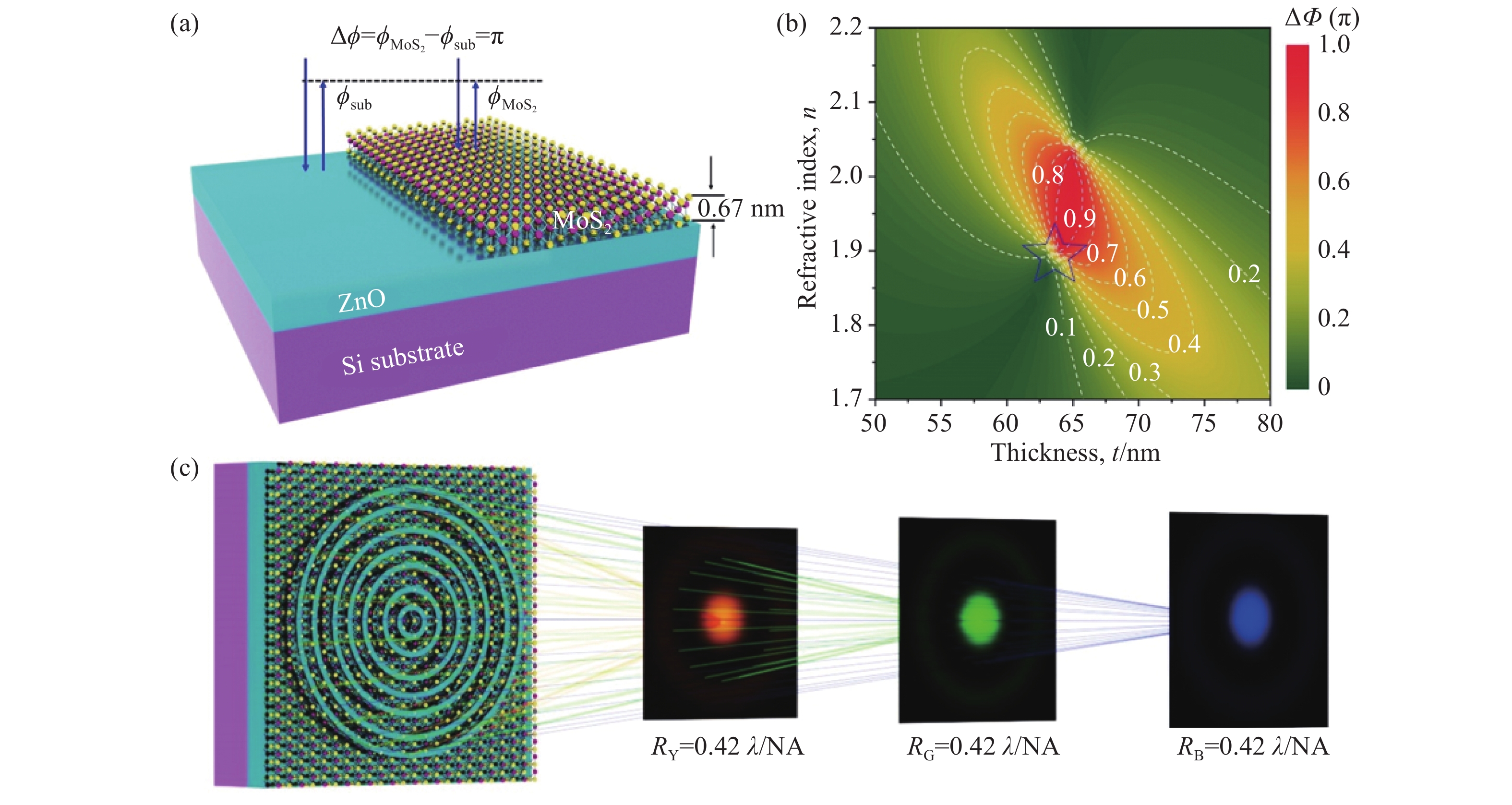
QIN F, LIU B Q, ZHU L W, et al. π-phase modulated monolayer supercritical lens[J]. Nature Communications, 2021, 12(1): 32. doi: 10.1038/s41467-020-20278-x
|
| [67] |
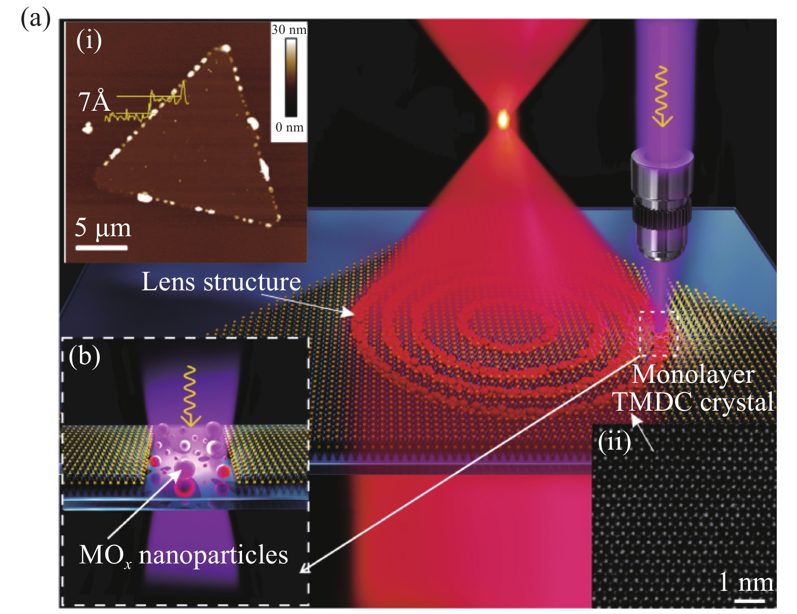
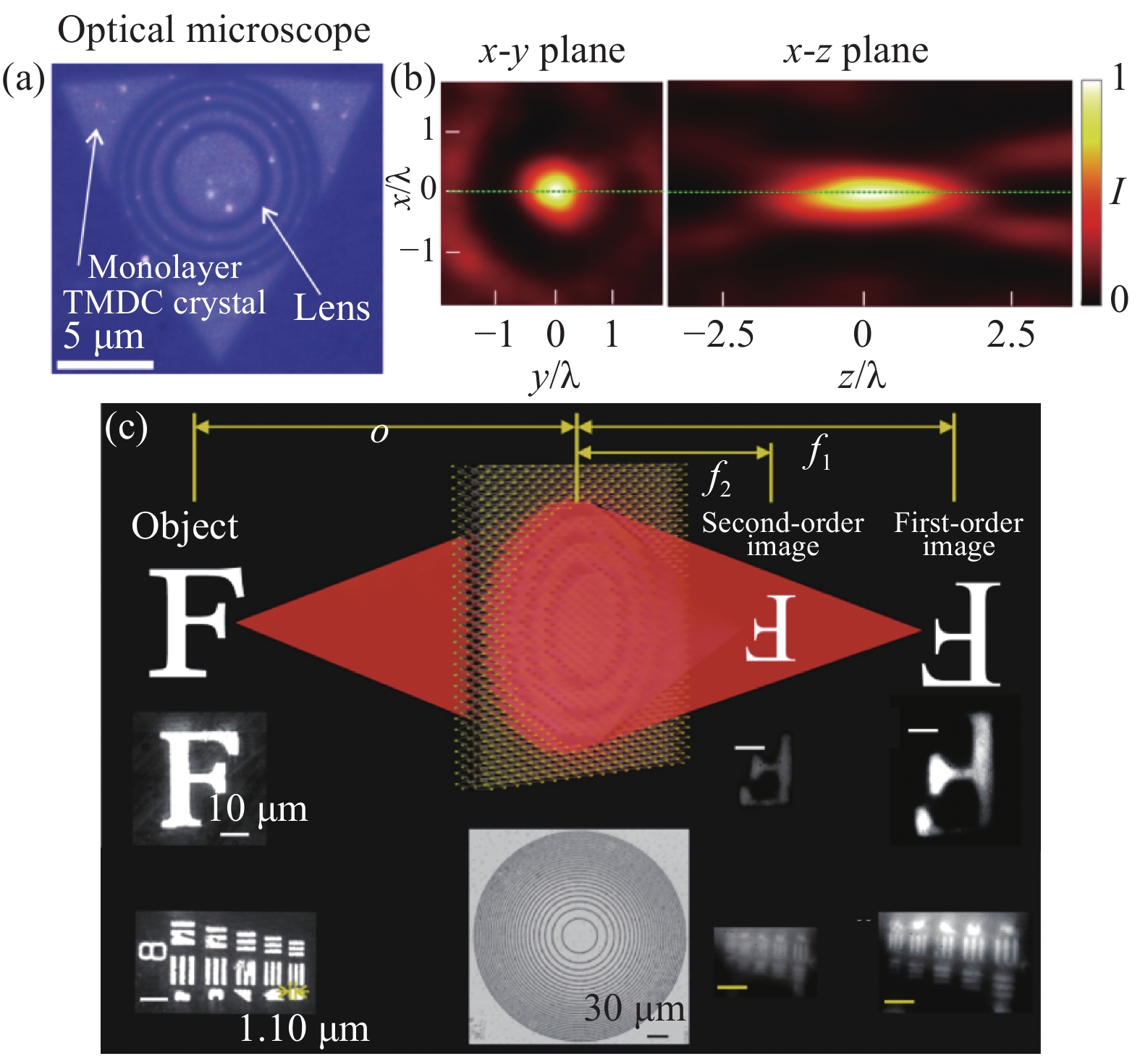
LIN H, XU Z Q, CAO G Y, et al. Diffraction-limited imaging with monolayer 2D material-based ultrathin flat lenses[J]. Light:Science &Applications, 2020, 9(1): 137.
|
| [68] |
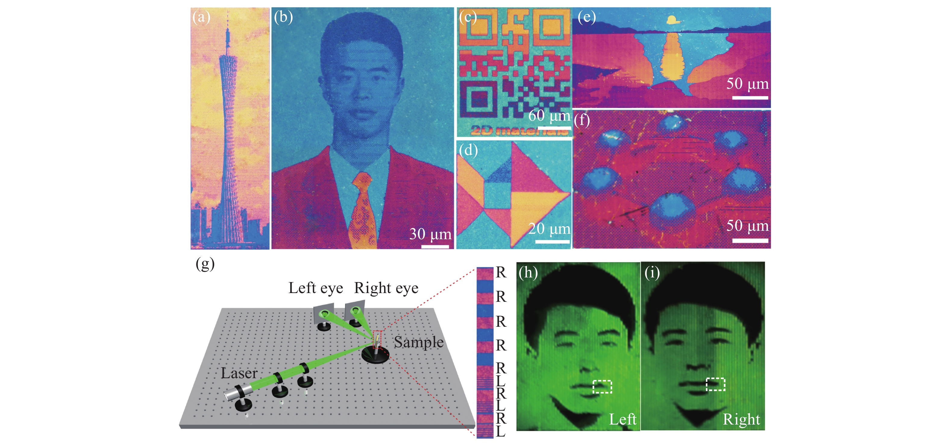
HU D J, LI H, ZHU Y P, et al. Ultra-sensitive nanometric flat laser prints for binocular stereoscopic image[J]. Nature Communications, 2021, 12(1): 1154. doi: 10.1038/s41467-021-21499-4
|
| [69] |
VAN DE GROEP J, SONG J H, CELANO U, et al. Exciton resonance tuning of an atomically thin lens[J]. Nature Photonics, 2020, 14(7): 426-430. doi: 10.1038/s41566-020-0624-y
|
| [70] |
QU CH, MA SH J, HAO J M, et al. Tailor the functionalities of metasurfaces based on a complete phase diagram[J]. Physical Review Letters, 2015, 115(23): 235503. doi: 10.1103/PhysRevLett.115.235503
|
| [71] |
LOPEZ-SANCHEZ O, LEMBKE D, KAYCI M, et al. Ultrasensitive photodetectors based on monolayer MoS2[J]. Nature Nanotechnology, 2013, 8(7): 497-501. doi: 10.1038/nnano.2013.100
|
| [72] |
ANDRZEJEWSKI D, HOPMANN E, JOHN M, et al. WS2 monolayer-based light-emitting devices in a vertical p–n architecture[J]. Nanoscale, 2019, 11(17): 8372-8379. doi: 10.1039/C9NR01573F
|
| [73] |
DOBUSCH L, SCHULER S, PEREBEINOS V, et al. Thermal light emission from monolayer MoS2[J]. Advanced Materials, 2017, 29(31): 1701304. doi: 10.1002/adma.201701304
|
| [74] |
YANG J, WANG ZH, WANG F, et al. Atomically thin optical lenses and gratings[J]. Light:Science &Applications, 2016, 5(3): e16046.
|
| [75] |
KATS M A, BLANCHARD R, GENEVET P, et al. Nanometre optical coatings based on strong interference effects in highly absorbing media[J]. Nature Materials, 2013, 12(1): 20-24. doi: 10.1038/nmat3443
|
| [76] |
WANG Z, YUAN G H, YANG M, et al. Exciton-enabled meta-optics in two-dimensional transition metal dichalcogenides[J]. Nano Letters, 2020, 20(11): 7964-7972. doi: 10.1021/acs.nanolett.0c02712
|
Figures(12)


 DownLoad: