| Citation: | ZHANG Jin-yue, LYU Jun-peng, NI Zhen-hua. Highly sensitive infrared detector based on a two-dimensional heterojunction[J]. Chinese Optics, 2021, 14(1): 87-99. doi: 10.37188/CO.2020-0139

|

| [1] |
WANG P, XIA H, Li Q, et al. Sensing infrared photons at room temperature: from bulk materials to atomic layers[J]. Small, 2019, 15(46): 1904396. doi: 10.1002/smll.201904396
|
| [2] |
WANG F K, ZHANG Y, GAO Y, et al. 2D metal Chalcogenides for IR photodetection[J]. Small, 2019, 15(30): 1901347. doi: 10.1002/smll.201901347
|
| [3] |
CHEN H Y, LIU H, ZHANG ZH M, et al. Nanostructured photodetectors: from ultraviolet to terahertz[J]. Advanced Materials, 2016, 28(3): 403-433. doi: 10.1002/adma.201503534
|
| [4] |
WANG X D, SHEN H, CHEN Y, et al. Multimechanism synergistic photodetectors with ultrabroad spectrum response from 375 nm to 10 µm[J]. Advanced Science, 2019, 6(15): 1901050. doi: 10.1002/advs.201901050
|
| [5] |
ROGALSKI A. HgCdTe infrared detector material: history, status and outlook[J]. Reports on Progress in Physics, 2005, 68(10): 2267-2336. doi: 10.1088/0034-4885/68/10/R01
|
| [6] |
LIN CH, ANSELM A, KUO C H, et al. Type-II InAs/InGaSb SL photodetectors[J]. Proceedings of SPIE, 2000, 3948: 133-144. doi: 10.1117/12.382112
|
| [7] |
GREIN C H, YOUNG P M, FLATTÉ M E, et al. Long wavelength InAs/InGaSb infrared detectors: optimization of carrier lifetimes[J]. Journal of Applied Physics, 1995, 78(12): 7143-7152. doi: 10.1063/1.360422
|
| [8] |
ROGALSKI A. Comparison of the performance of quantum well and conventional bulk infrared photodetectors[J]. Infrared Physics &Technology, 1997, 38(5): 295-310.
|
| [9] |
ZHANG Y G, GU Y, TIAN ZH B, et al. Wavelength extended 2.4 µm heterojunction InGaAs photodiodes with InAlAs cap and linearly graded buffer layers suitable for both front and back illuminations[J]. Infrared Physics &Technology, 2008, 51(4): 316-321.
|
| [10] |
RICHARDS P L. Bolometers for infrared and millimeter waves[J]. Journal of Applied Physics, 1994, 76(1): 1-24.
|
| [11] |
ROGALSKI A. Recent progress in infrared detector technologies[J]. Infrared Physics &Technology, 2011, 54(3): 136-154.
|
| [12] |
TAN CH L, CAO X H, WU X J, et al. Recent advances in ultrathin two-dimensional nanomaterials[J]. Chemical Reviews, 2017, 117(9): 6225-6331. doi: 10.1021/acs.chemrev.6b00558
|
| [13] |
JARIWALA D, MARKS T J, HERSAM M C. Mixed-dimensional van der Waals heterostructures[J]. Nature Materials, 2017, 16(2): 170-181. doi: 10.1038/nmat4703
|
| [14] |
MIRÓ P, AUDIFFRED M, HEINE T. An atlas of two-dimensional materials[J]. Chemical Society Reviews, 2014, 43(18): 6537-6554. doi: 10.1039/C4CS00102H
|
| [15] |
HU Y, CHEN T, WANG X Q, et al. Controlled growth and photoconductive properties of hexagonal SnS2 nanoflakes with mesa-shaped atomic steps[J]. Nano Research, 2017, 10(4): 1434-1447. doi: 10.1007/s12274-017-1525-3
|
| [16] |
HU Y, MAO L Y, YUAN X, et al. Controllable growth and flexible optoelectronic devices of regularly-assembled Bi2S3 semiconductor nanowire bifurcated junctions and crosslinked networks[J]. Nano Research, 2020, 13(8): 2226-2232. doi: 10.1007/s12274-020-2841-6
|
| [17] |
HU Y, QI ZH H, LU J Y, et al. Van der Waals epitaxial growth and interfacial passivation of two-dimensional single-crystalline few-layer gray arsenic nanoflakes[J]. Chemistry of Materials, 2019, 31(12): 4524-4535. doi: 10.1021/acs.chemmater.9b01151
|
| [18] |
WANG X X, HU Y, MO J B, et al. Arsenene: a potential therapeutic agent for acute Promyelocytic Leukaemia cells by acting on nuclear proteins[J]. Angewandte Chemie International Edition, 2020, 59(13): 5151-5158. doi: 10.1002/anie.201913675
|
| [19] |
BULLOCK J, AMANI M, CHO J, et al. Polarization-resolved black phosphorus/molybdenum disulfide mid-wave infrared photodiodes with high detectivity at room temperature[J]. Nature Photonics, 2018, 12(10): 601-607. doi: 10.1038/s41566-018-0239-8
|
| [20] |
GAO A Y, LAI J W, WANG Y J, et al. Observation of ballistic avalanche phenomena in nanoscale vertical InSe/BP heterostructures[J]. Nature Nanotechnology, 2019, 14(3): 217-222. doi: 10.1038/s41565-018-0348-z
|
| [21] |
CASTELLANOS-GOMEZ A, BARKELID M, GOOSSENS A M, et al. Laser-thinning of MoS2: on demand generation of a single-layer semiconductor[J]. Nano Letters, 2012, 12(6): 3187-3192. doi: 10.1021/nl301164v
|
| [22] |
MATTHEISS L F. Band structures of transition-metal-dichalcogenide layer compounds[J]. Physical Review B, 1973, 8(8): 3719-3740. doi: 10.1103/PhysRevB.8.3719
|
| [23] |
CASTELLANOS-GOMEZ A. Black phosphorus: narrow gap, wide applications[J]. The Journal of Physical Chemistry Letters, 2015, 6(21): 4280-4291. doi: 10.1021/acs.jpclett.5b01686
|
| [24] |
LONG M SH, WANG P, FANG H H, et al. Progress, challenges, and opportunities for 2D material based photodetectors[J]. Advanced Functional Materials, 2019, 29(19): 1803807. doi: 10.1002/adfm.201803807
|
| [25] |
NOVOSELOV K S, FAL'KO V I, COLOMBO L, et al. A roadmap for Graphene[J]. Nature, 2012, 490(7419): 192-200. doi: 10.1038/nature11458
|
| [26] |
ALLEN M J, TUNG V C, KANER R B. Honeycomb carbon: a review of Graphene[J]. Chemical Reviews, 2010, 110(1): 132-145. doi: 10.1021/cr900070d
|
| [27] |
SUN ZH H, LIU ZH K, LI J H, et al. Infrared photodetectors based on CVD-grown graphene and PbS quantum dots with ultrahigh responsivity[J]. Advanced Materials, 2012, 24(43): 5878-5883. doi: 10.1002/adma.201202220
|
| [28] |
ZHANG Y ZH, LIU T, MENG B, et al. Broadband high photoresponse from pure monolayer graphene photodetector[J]. Nature Communications, 2013, 4(1): 1811. doi: 10.1038/ncomms2830
|
| [29] |
KONSTANTATOS G, BADIOLI M, GAUDREAU L, et al. Hybrid graphene-quantum dot phototransistors with ultrahigh gain[J]. Nature Nanotechnology, 2012, 7(6): 363-368. doi: 10.1038/nnano.2012.60
|
| [30] |
GROTEVENT M J, HAIL C U, YAKUNIN S, et al. Nanoprinted quantum dot-graphene photodetectors[J]. Advanced Optical Materials, 2019, 7(11): 1900019. doi: 10.1002/adom.201900019
|
| [31] |
KOPPENS F H L, MUELLER T, AVOURIS P, et al. Photodetectors based on graphene, other two-dimensional materials and hybrid systems[J]. Nature Nanotechnology, 2014, 9(10): 780-793. doi: 10.1038/nnano.2014.215
|
| [32] |
CLIFFORD J P, KONSTANTATOS G, JOHNSTON K W, et al. Fast, sensitive and spectrally tuneable colloidal-quantum-dot photodetectors[J]. Nature Nanotechnology, 2009, 4(1): 40-44. doi: 10.1038/nnano.2008.313
|
| [33] |
KONSTANTATOS G. Current status and technological prospect of photodetectors based on two-dimensional materials[J]. Nature Communications, 2018, 9(1): 5266. doi: 10.1038/s41467-018-07643-7
|
| [34] |
NIKITSKIY I, GOOSSENS S, KUFER D, et al. Integrating an electrically active colloidal quantum dot photodiode with a graphene phototransistor[J]. Nature Communications, 2016, 7(1): 11954. doi: 10.1038/ncomms11954
|
| [35] |
CHEN X Q, LIU X L, WU B, et al. Improving the performance of graphene phototransistors using a heterostructure as the light-absorbing layer[J]. Nano Letters, 2017, 17(10): 6391-6396. doi: 10.1021/acs.nanolett.7b03263
|
| [36] |
BUSCEMA M, ISLAND J O, GROENENDIJK D J, et al. Photocurrent generation with two-dimensional van der waals semiconductors[J]. Chemical Society Reviews, 2015, 44(11): 3691-3718. doi: 10.1039/C5CS00106D
|
| [37] |
TANAKA A, MATSUMOTO S, TSUKAMOTO N, et al. Infrared focal plane array incorporating silicon IC process compatible bolometer[J]. IEEE Transactions on Electron Devices, 1996, 43(11): 1844-1850. doi: 10.1109/16.543017
|
| [38] |
MATHER J C. Bolometers: ultimate sensitivity, optimization, and amplifier coupling[J]. Applied Optics, 1984, 23(4): 584-588. doi: 10.1364/AO.23.000584
|
| [39] |
解光勇. 光电探测器噪声特性分析[J]. 信息技术,2008(11):8-10. doi: 10.3969/j.issn.1009-2552.2008.11.003
XIE G Y. Noise analysis for optoelectronic detector[J]. Information Technology, 2008(11): 8-10. (in Chinese) doi: 10.3969/j.issn.1009-2552.2008.11.003
|
| [40] |
王彦, 袁家虎. 一种提高CCD探测灵敏度的方法[J]. 光电工程,2000,27(6):5-8, 65. doi: 10.3969/j.issn.1003-501X.2000.06.002
WANG Y, YUAN J H. A method for improving the CCD sensitivity[J]. Opto-Electronic Engineering, 2000, 27(6): 5-8, 65. (in Chinese) doi: 10.3969/j.issn.1003-501X.2000.06.002
|
| [41] |
SZE S M, NG K K. Physics of Semiconductor Devices[M]. New York: John Wiley & Sons, 2006.
|
| [42] |
LONG M SH, LIU E F, WANG P, et al. Broadband photovoltaic detectors based on an atomically thin heterostructure[J]. Nano Letters, 2016, 16(4): 2254-2259. doi: 10.1021/acs.nanolett.5b04538
|
| [43] |
WANG L, JIE J SH, SHAO ZH B, et al. MoS2/Si heterojunction with vertically standing layered structure for ultrafast, high-detectivity, self-driven visible-near infrared photodetectors[J]. Advanced Functional Materials, 2015, 25(19): 2910-2919. doi: 10.1002/adfm.201500216
|
| [44] |
WU D, WANG Y G, ZENG L H, et al. Design of 2D layered PtSe2 heterojunction for the high-performance, room-temperature, broadband, infrared photodetector[J]. ACS Photonics, 2018, 5(9): 3820-3827. doi: 10.1021/acsphotonics.8b00853
|
| [45] |
JIA CH, WU D, WU E P, et al. A self-powered high-performance photodetector based on a MoS2/GaAs heterojunction with high polarization sensitivity[J]. Journal of Materials Chemistry C, 2019, 7(13): 3817-3821. doi: 10.1039/C8TC06398B
|
| [46] |
HOLLENHORST J N. Ballistic avalanche photodiodes: ultralow noise avalanche diodes with nearly equal ionization probabilities[J]. Applied Physics Letters, 1986, 49(9): 516-518. doi: 10.1063/1.97106
|
| [47] |
JINDAL R P. Approaching fundamental limits on signal detection[J]. IEEE Transactions on Electron Devices, 1994, 41(11): 2133-2138. doi: 10.1109/16.333833
|
| [48] |
WANG Y G, HUANG X W, WU D, et al. A room-temperature near-infrared photodetector based on a MoS2/CdTe p-n heterojunction with a broadband response up to 1700 nm[J]. Journal of Materials Chemistry C, 2018, 6(18): 4861-4865. doi: 10.1039/C8TC01237G
|
| [49] |
ZENG L H, LIN SH H, LOU ZH H, et al. Ultrafast and sensitive photodetector based on a PtSe2/Silicon nanowire array heterojunction with a multiband spectral response from 200 to 1550 nm[J]. NPG ASIA Materials, 2018, 10(4): 352-362. doi: 10.1038/s41427-018-0035-4
|
| [50] |
ZHANG T F, LI ZH P, WANG J ZH, et al. Broadband photodetector based on carbon nanotube thin film/single layer graphene Schottky junction[J]. Scientific Reports, 2016, 6(1): 38569. doi: 10.1038/srep38569
|
| [51] |
XIAO P, MAO J, DING K, et al. Solution-processed 3D RGO-MoS2/Pyramid Si heterojunction for ultrahigh detectivity and ultra-broadband photodetection[J]. Advanced Materials, 2018, 30(31): 1801729. doi: 10.1002/adma.201801729
|
| [52] |
WU E P, WU D, JIA CH, et al. In situ fabrication of 2D WS2/Si type-II heterojunction for self-powered broadband photodetector with response up to mid-infrared[J]. ACS Photonics, 2019, 6(2): 565-572. doi: 10.1021/acsphotonics.8b01675
|
| [53] |
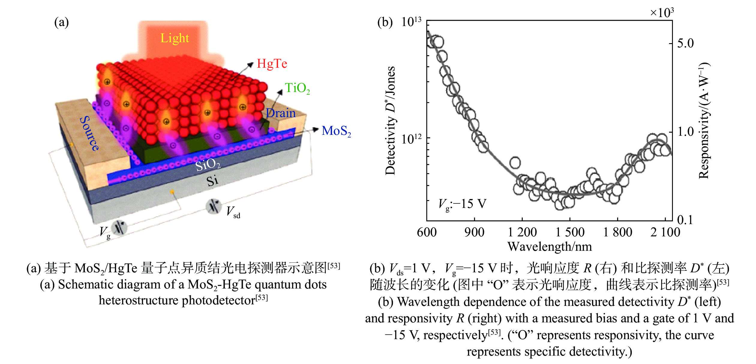
HUO N J, GUPTA S, KONSTANTATOS G. MoS2-HgTe quantum dot hybrid photodetectors beyond 2 µm[J]. Advanced Materials, 2017, 29(17): 1606576. doi: 10.1002/adma.201606576
|
| [54] |
YE L, WANG P, LUO W J, et al. Highly polarization sensitive infrared photodetector based on black phosphorus-on-WSe2 photogate vertical heterostructure[J]. Nano Energy, 2017, 37: 53-60. doi: 10.1016/j.nanoen.2017.05.004
|
| [55] |
KUFER D, NIKITSKIY I, LASANTA T, et al. Hybrid 2D-0D MoS2-PbS quantum dot photodetectors[J]. Advanced Materials, 2015, 27(1): 176-180. doi: 10.1002/adma.201402471
|
| [56] |
QI ZH Y, YANG T F, LI D, et al. High-responsivity two-dimensional p-Pbi2/n-WS2 vertical heterostructure photodetectors enhanced by photogating effect[J]. Materials Horizons, 2019, 6(7): 1474-1480. doi: 10.1039/C9MH00335E
|
| [57] |
GUO N, GONG F, LIU J K, et al. Hybrid WSe2-In2O3 phototransistor with ultrahigh detectivity by efficient suppression of dark currents[J]. ACS Applied Materials &Interfaces, 2017, 9(39): 34489-34496.
|
| [58] |
YEH C H, CHEN H C, LIN H C, et al. Ultrafast monolayer In/Gr-WS2-Gr hybrid photodetectors with high gain[J]. ACS Nano, 2019, 13(3): 3269-3279. doi: 10.1021/acsnano.8b09032
|
| [59] |
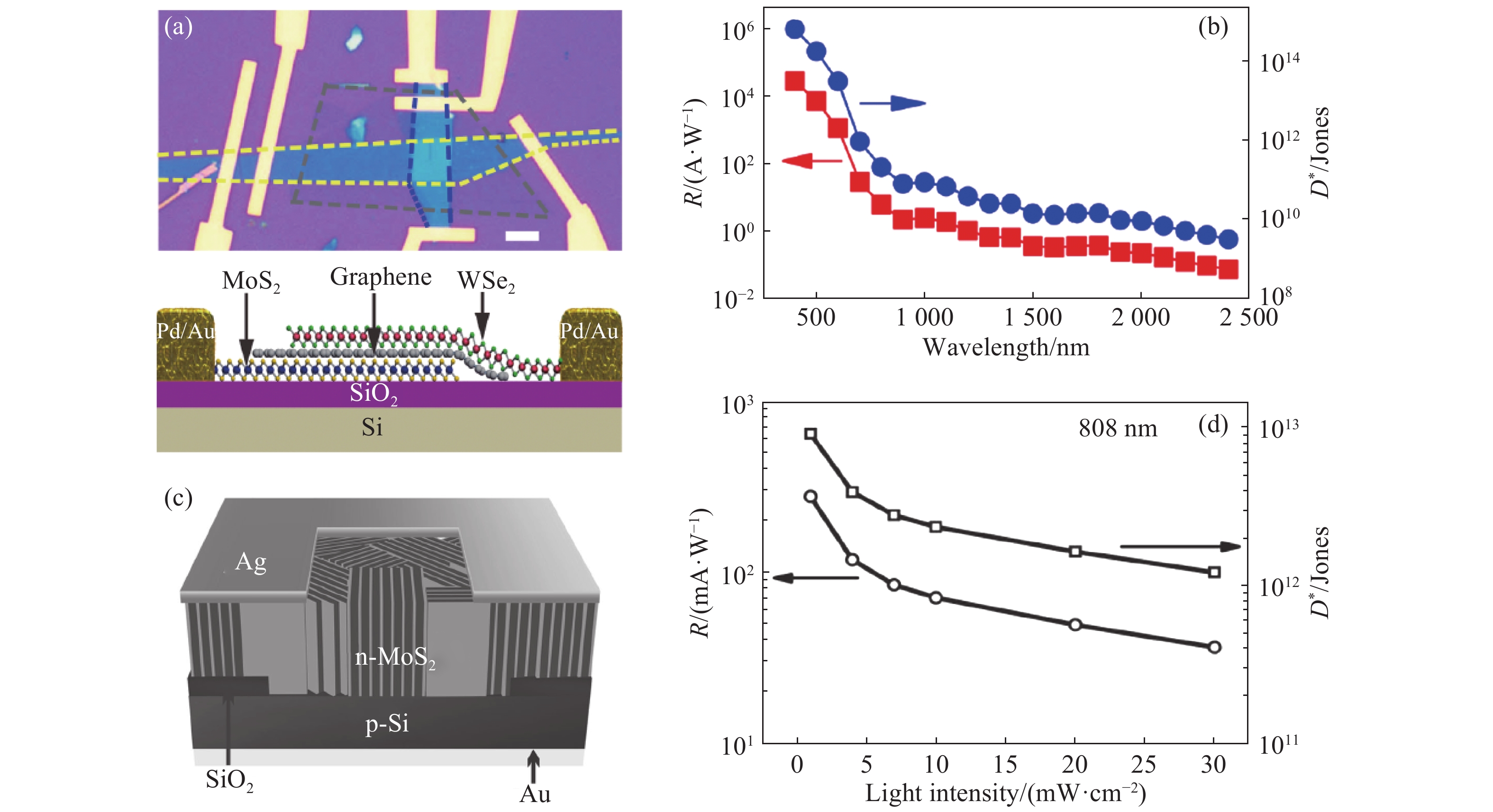
LONG M SH, WANG Y, WANG P, et al. Palladium diselenide long-wavelength infrared photodetector with high sensitivity and stability[J]. ACS Nano, 2019, 13(2): 2511-2519.
|
Figures(2) / Tables(1)


 DownLoad: