


Method for the simultaneous measurement of waveguide propagation loss and bending loss
doi: 10.37188/CO.EN.2022-0027
-
摘要:
波导的传输损耗是评价集成光学平台性能的一个关键指标。常用的测量传输损耗的cut-back测试方法需引入弯曲波导测试结构。为了去除弯曲损耗的影响,通常会将弯曲半径设计的足够大,但这样会占用很多的版图面积。本文基于铌酸锂平台提出了一种可以同时测试波导传输损耗和弯曲损耗的方法。通过仿真发现波导弯曲损耗与弯曲半径成指数关系,对弯曲损耗取对数值后,与弯曲半径成线性关系。利用遗传算法拟合cut-back结构的插入损耗曲线,并计算得到波导的传输损耗和弯曲损耗。用该方法测量铌酸锂波导,在1550 nm波长下得到0.558 dB/cm的传输损耗和100 μm弯曲半径下0.698 dB/90°的弯曲损耗。利用这种方法可以同时测试波导的传输损耗和弯曲损耗,还可以大大节省占地面积。
Abstract:The propagation loss of a waveguide is a key indicator to evaluate the performance of an integrated optical platform. The commonly used cut-back method for measuring propagation loss requires the introduction of the spiral test structure. In order to remove bending loss, the bending radius is usually designed to be larger but this consequently has a larger footprint. In this paper, we suggested a method to simultaneously measure the propagation loss and bending loss of waveguides with a cut-back structure. According to simulations, the bending loss can be exponentially fitted with the bending radius, which can be further simplified as linear fitting between the natural logarithm of the bending loss and bending radius. A genetic algorithm was used to fit the insertion loss curve of the cut-back structure and the propagation losses and bending loss were calculated. With this method, we measured a cut-back structure of lithium niobate waveguide and got a propagation loss of 0.558 dB/cm and a bending loss of 0.698 dB/90° at a radius of 100 μm and wavelength of 1550 nm. Using this method, we can simultaneously measure waveguide propagation loss and bending loss while mitigating the footprint.
-
Key words:
- propagation loss /
- bending loss /
- lithium niobate /
- genetic algorithm
-

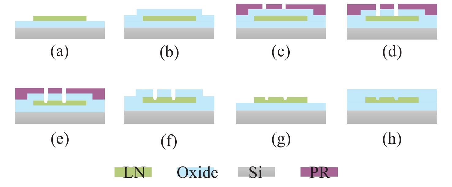
Figure 1. Process flow of LN waveguide fabrication. (a) LNOI substrate. (b) Deposition of oxide by PECVD. (c) I-line lithography. (d) Hard mask etching. (e) LN etching. (f) Photoresist removal. (g) Hard mask removal. (h) Deposition of cladding by PECVD
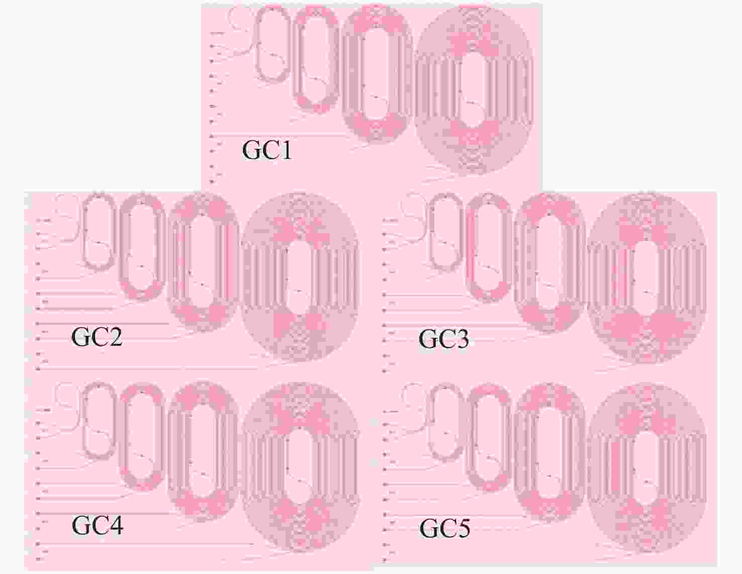
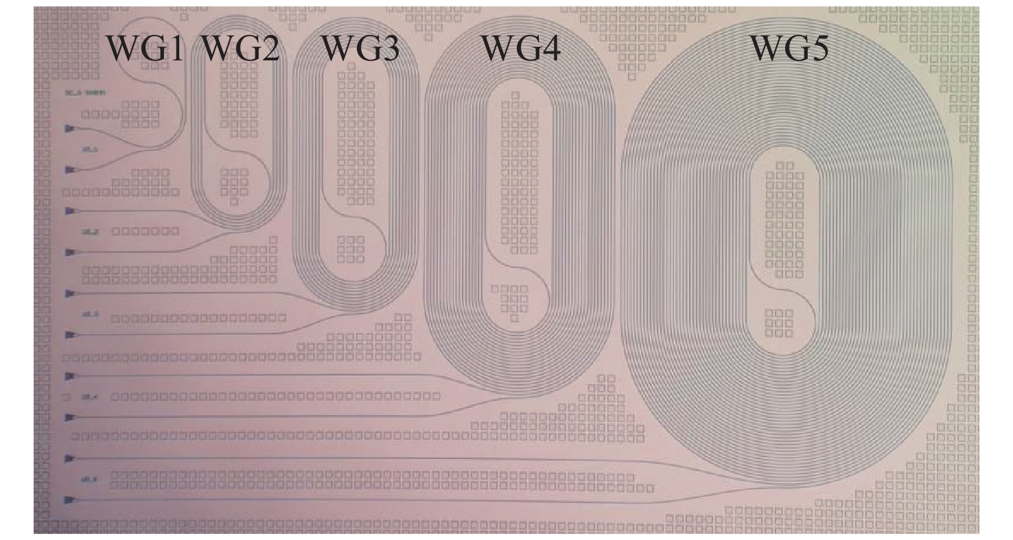
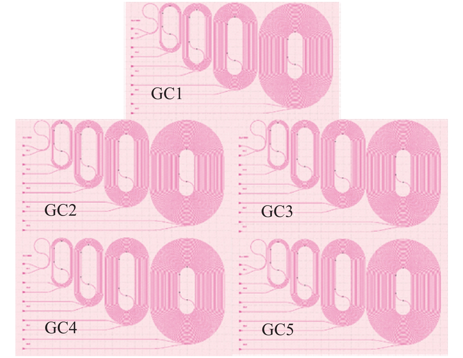
Figure 4. Layout image of the 5 sets of cutback structures for the 5 splits of the grating coupler
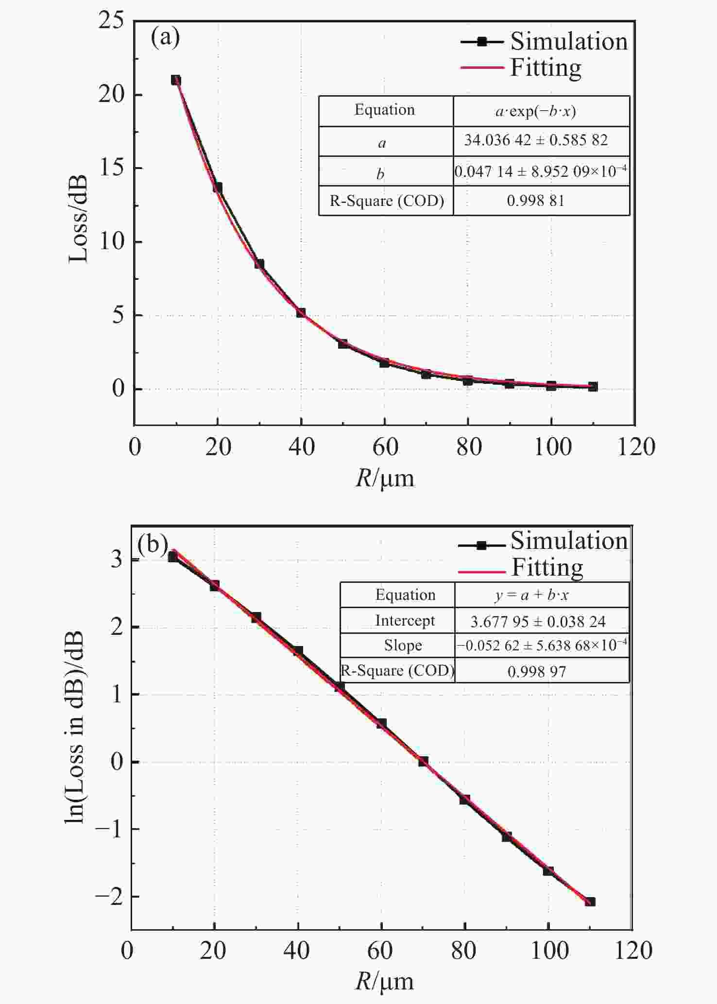
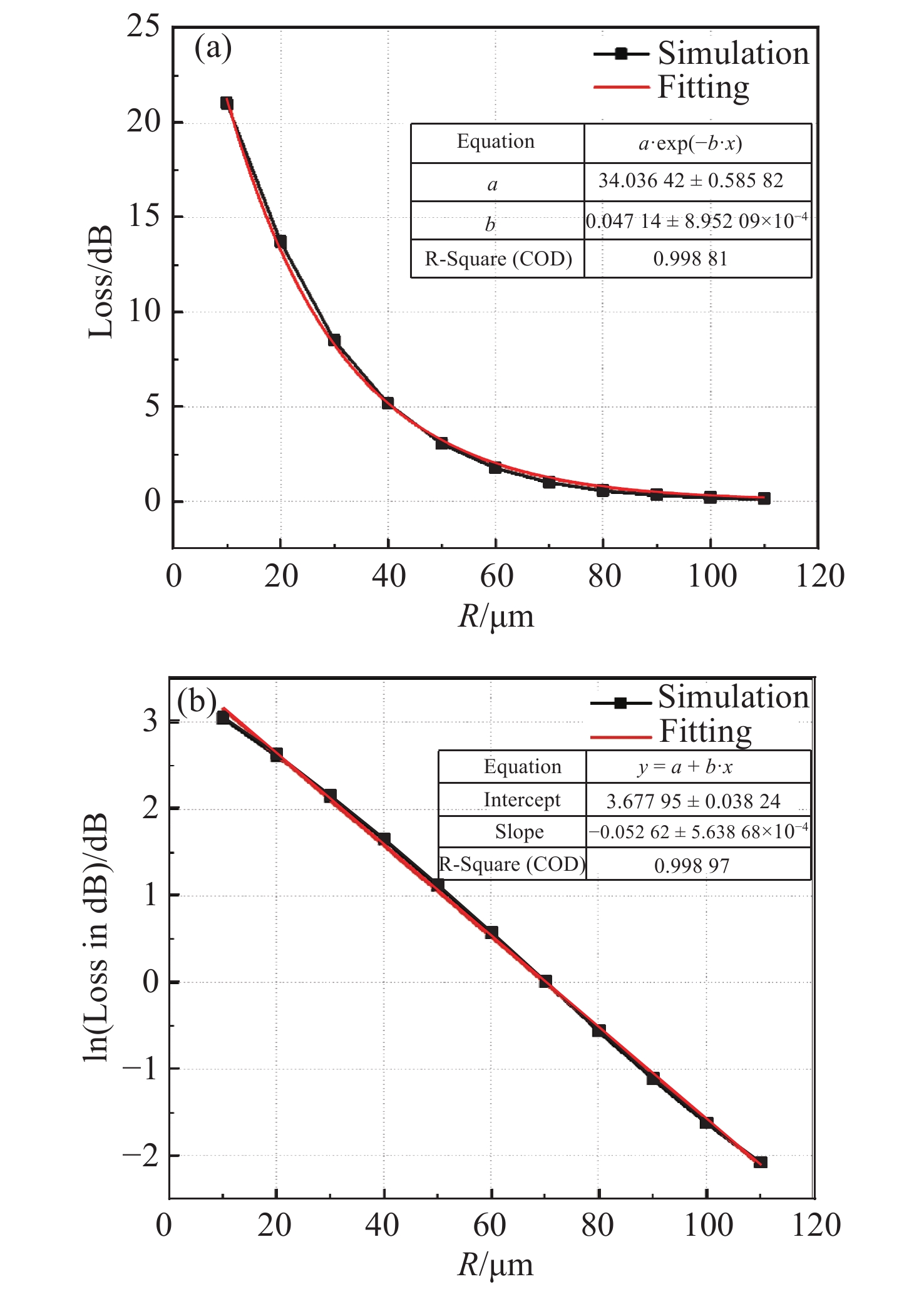
Figure 5. (a) Simulation of the bending loss of the LN waveguide. The bending loss of the waveguide is exponentially related to the bending radius. (b) The linear fitting of the natural logarithm of the bending loss with the bending radius
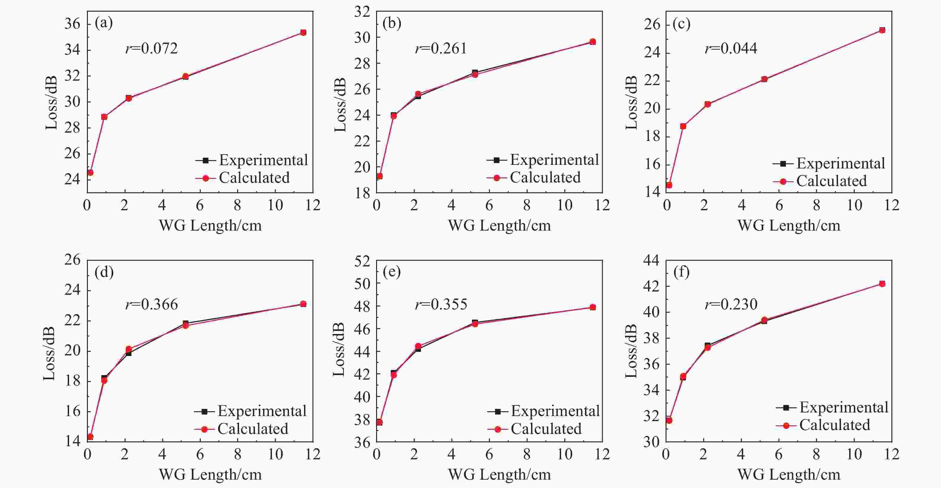
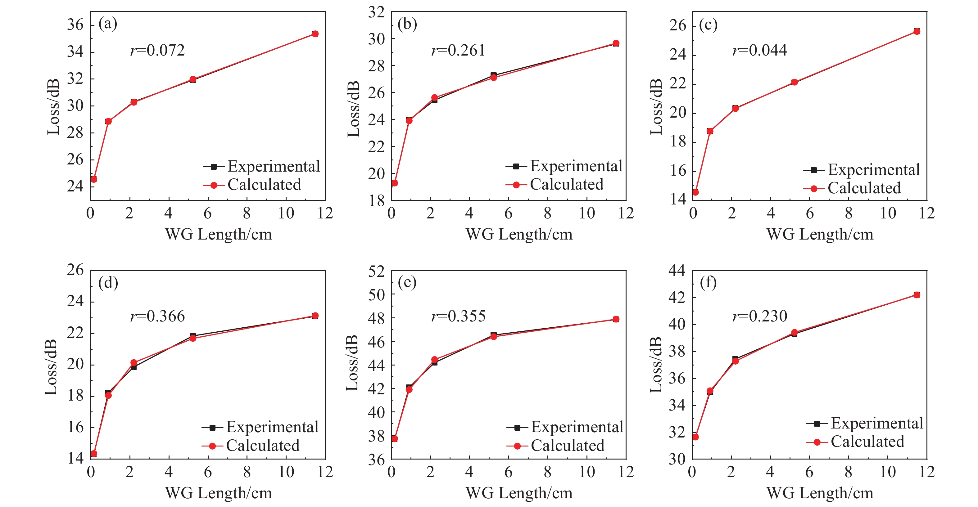
Figure 7. The measurement results of the cut-back structure and the fitting results. (a) GC1, (b) GC2, (c) GC3, (d) GC4, (e) GC5-1, (f) GC5-2
Table 1. The basic information of the cut-back structure
Length(cm) The radius of bend(μm) Number of radius WG1 0.1582 100, 110 100×4,110×2 WG2 0.9021 100,110,120,130,140,150 (100-140)×4,150×2 WG3 2.2054 100,110,120…190,200 (100-190) ×4,200×2 WG4 5.2274 100,110,120…290,300 (100-290) ×4,300×2 WG5 11.4854 100,110,120…490,500 (100-490) ×4,500×2  下载: 导出CSV
Table 2. The summary of the fitting results
α(dB/cm) αb0(dB) k αgc(dB) r GC1 0.538 0.805 0.0446 20.220 0.072 GC2 0.408 0.698 0.0346 15.448 0.261 GC3 0.558 0.698 0.0399 10.740 0.044 GC4 0.209 0.393 0.0201 12.114 0.366 GC5-1 0.194 0.416 0.0176 35.350 0.355 GC5-2 0.421 0.339 0.0194 29.666 0.230
下载: 导出CSV
Table 3. The performance comparison of different measurement methods
Advantages Disadvantages Traditional cut-back[33] Widely employed owing to its ease of use. Can’t simultaneously measure the propagation loss and bending loss;
Requires identical
coupling conditions.Three-prism Method[34] Does not require constant coupling conditions Has low measurement accuracy. Fabry-Perot transmission method[35] Can eliminate the influence of
coupling loss and has higher accuracyRequires a complex coupling system. This paper Can simultaneously measure waveguide propagation loss and bending loss;
Smaller footprint;
Simple and convenient operation.
下载: 导出CSV
-
[1] ARIZMENDI L. Photonic applications of lithium niobate crystals[J]. Physica Status Solidi (A), 2004, 201(2): 253-283. doi: 10.1002/pssa.200303911 [2] WEIS R S, GAYLORD T K. Lithium niobate: summary of physical properties and crystal structure[J]. Applied Physics A, 1985, 37(4): 191-203. doi: 10.1007/BF00614817 [3] WU R B, WANG M, XU J, et al.. Long low-loss-litium niobate on insulator waveguides with sub-nanometer surface roughness[J]. Nanomaterials, 2018, 8(11): 910. doi: 10.3390/nano8110910 [4] ZHU D, SHAO L B, YU M J, et al.. Integrated photonics on thin-film lithium niobate[J]. Advances in Optics and Photonics, 2021, 13(2): 242-352. doi: 10.1364/AOP.411024 [5] RABIEI P, GUNTER P. Optical and electro-optical properties of submicrometer lithium niobate slab waveguides prepared by crystal ion slicing and wafer bonding[J]. Applied Physics Letters, 2004, 85(20): 4603-4605. doi: 10.1063/1.1819527 [6] POBERAJ G, HU H, SOHLER W, et al.. Lithium niobate on insulator (LNOI) for micro-photonic devices[J]. Laser & Photonics Reviews, 2012, 6(4): 488-503. [7] LEVY M, RADOJEVIC A M. Single-crystal lithium niobate films by crystal ion slicing[M]//ALEXE M, GÖSELE U. Wafer Bonding: Applications and Technology. Berlin: Springer, 2004: 417-450. [8] ZHANG M, BUSCAINO B, WANG CH, et al.. Broadband electro-optic frequency comb generation in a lithium niobate microring resonator[J]. Nature, 2019, 568(7752): 373-377. doi: 10.1038/s41586-019-1008-7 [9] XU M Y, HE M B, ZHANG H G, et al.. High-performance coherent optical modulators based on thin-film lithium niobate platform[J]. Nature Communications, 2020, 11(1): 3911. doi: 10.1038/s41467-020-17806-0 [10] WANG CH, ZHANG M, CHEN X, et al.. Integrated lithium niobate electro-optic modulators operating at CMOS-compatible voltages[J]. Nature, 2018, 562(7725): 101-104. doi: 10.1038/s41586-018-0551-y [11] WANG CH, LANGROCK C, MARANDI A, et al.. Ultrahigh-efficiency wavelength conversion in nanophotonic periodically poled lithium niobate waveguides[J]. Optica, 2018, 5(11): 1438-1441. doi: 10.1364/OPTICA.5.001438 [12] LIN J T, YAO N, HAO ZH ZH, et al.. Broadband quasi-phase-matched harmonic generation in an on-chip monocrystalline lithium niobate microdisk resonator[J]. Physical Review Letters, 2019, 122(17): 173903. doi: 10.1103/PhysRevLett.122.173903 [13] HE M B, XU M Y, REN Y X, et al.. High-performance hybrid silicon and lithium niobate Mach–Zehnder modulators for 100 Gbit s−1 and beyond[J]. Nature Photonics, 2019, 13(5): 359-364. doi: 10.1038/s41566-019-0378-6 [14] CAI L T, KONG R R, WANG Y W, et al.. Channel waveguides and y-junctions in x-cut single-crystal lithium niobate thin film[J]. Optics Express, 2015, 23(22): 29211-29221. doi: 10.1364/OE.23.029211 [15] CAI L T, WANG Y W, HU H. Low-loss waveguides in a single-crystal lithium niobate thin film[J]. Optics Letters, 2015, 40(13): 3013-3016. doi: 10.1364/OL.40.003013 [16] HU H, YANG J, GUI L, et al.. Lithium niobate-on-insulator (LNOI): status and perspectives[J]. Proceedings of SPIE, 2012, 8431: 84311D. [17] KRASNOKUTSKA I, TAMBASCO J L J, LI X J, et al.. Ultra-low loss photonic circuits in lithium niobate on insulator[J]. Optics Express, 2018, 26(2): 897-904. doi: 10.1364/OE.26.000897 [18] ULLIAC G, COURJAL N, CHONG H M H, et al.. Batch process for the fabrication of LiNbO3 photonic crystals using proton exchange followed by CHF3 reactive ion etching[J]. Optical Materials, 2008, 31(2): 196-200. doi: 10.1016/j.optmat.2008.03.004 [19] DONG P, QIAN W, LIAO SH R, et al.. Low loss shallow-ridge silicon waveguides[J]. Optics Express, 2010, 18(14): 14474-14479. doi: 10.1364/OE.18.014474 [20] GUTIERREZ A M, BRIMONT A, AAMER M, et al.. Method for measuring waveguide propagation losses by means of a Mach–Zehnder Interferometer structure[J]. Optics Communications, 2012, 285(6): 1144-1147. doi: 10.1016/j.optcom.2011.11.064 [21] TAEBI S, KHORASANINEJAD M, SAINI S S. Modified fabry-perot interferometric method for waveguide loss measurement[J]. Applied Optics, 2008, 47(35): 6625-6630. doi: 10.1364/AO.47.006625 [22] HE Y M, LI ZH S, LU D. A waveguide loss measurement method based on the reflected interferometric pattern of a Fabry-Perot cavity[J]. Proceedings of SPIE, 2018, 10535: 105351U. [23] HOLLAND J H. Adaptation in Natural and Artificial Systems: An Introductory Analysis with Applications to Biology, Control, and Artificial Intelligence[M]. Cambridge: The MIT Press, 1992. [24] ALONSO J M, ALVARRUIZ F, DESANTES J M, et al.. Combining neural networks and genetic algorithms to predict and reduce diesel engine emissions[J]. IEEE Transactions on Evolutionary Computation, 2007, 11(1): 46-55. doi: 10.1109/TEVC.2006.876364 [25] VERMA R, LAKSHMINIARAYANAN P A. A case study on the application of a genetic algorithm for optimization of engine parameters[J]. Proceedings of the Institution of Mechanical Engineers, Part D: Journal of Automobile Engineering, 2006, 220(4): 471-479. [26] BAHADORI M, NIKDAST M, CHENG Q X, et al.. Universal design of waveguide bends in silicon-on-insulator photonics platform[J]. Journal of Lightwave Technology, 2019, 37(13): 3044-3054. doi: 10.1109/JLT.2019.2909983 [27] THYAGARAJAN K, SHENOY M R, GHATAK A K. Accurate numerical method for the calculation of bending loss in optical waveguides using a matrix approach[J]. Optics Letters, 1987, 12(4): 296-298. doi: 10.1364/OL.12.000296 [28] HAN ZH H, ZHANG P, BOZHEVOLNYI S I. Calculation of bending losses for highly confined modes of optical waveguides with transformation optics[J]. Optics Letters, 2013, 38(11): 1778-1780. doi: 10.1364/OL.38.001778 [29] STENGER V E, TONEY J, PONICK A, et al. Low loss and low vpi thin film lithium niobate on quartz electro-optic modulators[C]. 2017 European Conference on Optical Communication (ECOC), IEEE, 2017: 1-3. [30] LI X P, CHEN K X, HU ZH F. Low-loss bent channel waveguides in lithium niobate thin film by proton exchange and dry etching[J]. Optical Materials Express, 2018, 8(5): 1322-1327. doi: 10.1364/OME.8.001322 [31] REN T H, ZHANG M, WANG CH, et al.. An integrated low-voltage broadband lithium niobate phase modulator[J]. IEEE Photonics Technology Letters, 2019, 31(11): 889-892. doi: 10.1109/LPT.2019.2911876 [32] DING T T, ZHENG Y L, CHEN X F. On-chip solc-type polarization control and wavelength filtering utilizing periodically poled lithium niobate on insulator ridge waveguide[J]. Journal of Lightwave Technology, 2019, 37(4): 1296-1300. doi: 10.1109/JLT.2019.2892317 [33] VLASOV Y A, MCNAB S J. Losses in single-mode silicon-on-insulator strip waveguides and bends[J]. Optics Express, 2004, 12(8): 1622-1631. doi: 10.1364/OPEX.12.001622 [34] WON Y H, JAUSSAUD P C, CHARTIER G H. Three-prism loss measurements of optical waveguides[J]. Applied Physics Letters, 1980, 37(3): 269-271. doi: 10.1063/1.91903 [35] REGENER R, SOHLER W. Loss in low-finesse Ti: LiNbO3 optical waveguide resonators[J]. Applied Physics B, 1985, 36(3): 143-147. -

 下载:
下载:

计量
- 文章访问数: 878
- HTML全文浏览量: 474
- PDF下载量: 285
- 被引次数: 0
