InGaAs/AlGaAs quantum well intermixing induced by Si impurities under multi-variable conditions
doi: 10.37188/CO.2022-0257
-
摘要:
腔面光学灾变损伤是导致高功率量子阱半导体激光器阈值输出功率受限制的关键因素。通过量子阱混杂技术调整半导体激光器腔面局部区域处有源区材料的带隙宽度,形成对输出光透明的非吸收窗口,可提高激光器输出功率。本文基于InGaAs/AlGaAs高功率量子阱半导体激光器初级外延片,以外延Si单晶层作为扩散源,结合快速热退火方法开展了杂质诱导量子阱混杂研究。探索了介质层生长温度、介质层厚度、热处理温度、热处理时间等条件对混杂效果的影响。结果表明,50 nm的650 °C低温外延Si介质层并结合875 °C/90 s快速热退火处理可在保证光致发光谱的同时获得约57 nm的波长蓝移量。能谱测试发现,Si杂质扩散到初级外延片上的波导层是导致量子阱混杂效果显著的关键。
Abstract:Catastrophic Optical Mirror Damage (COMD) on the cavity surface is the key factor limiting the threshold output power of high-power quantum well semiconductor laser diodes. To improve the output power of the laser diode, the band gap width of the active material in the cavity surface of the semiconductor laser diode can be adjusted by the quantum well intermixing technology to form a non-absorbing window transparent to the output laser. Based on the primary epitaxial wafers of InGaAs/AlGaAs high power quantum well semiconductor laser diode, using the single crystal Si dielectric layer grown by Metal Oxide Chemical Vapor Deposition (MOCVD) as the diffusion source, the research on Si impurity induced quantum well intermixing was carried out by using the Rapid Thermal Annealing (RTA) process. The effects of growth characteristics of Si dielectric layer, the temperature and time of RTA on the intermixing process were investigated. The experimental results show that the epitaxial 50 nm Si dielectric layer at 650 °C combined with 875 °C/90 s RTA treatment can obtain about 57 nm wavelength blue shift while maintaining the photoluminescence spectrum shape and the primary epitaxial wafers. It is found that the diffusion of Si impurities into the waveguide layer on the primary epitaxial wafer is the key to the remarkable effect of quantum well intermixing by the energy spectrum measurement technique.
-
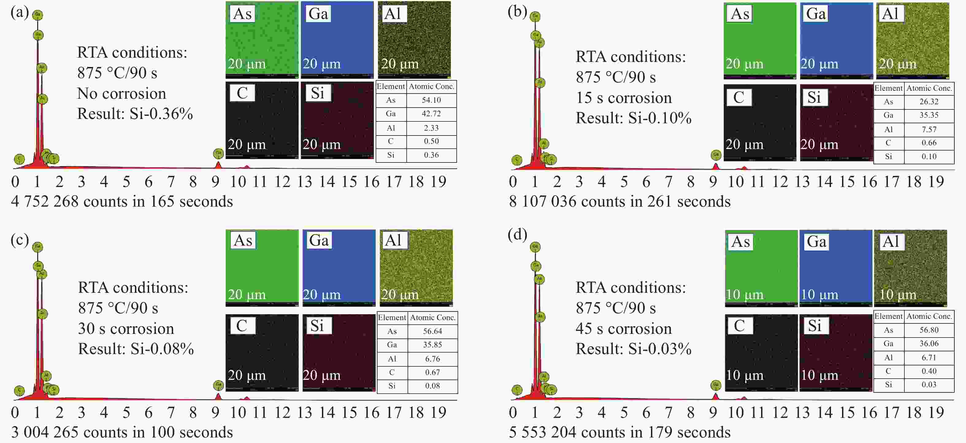
图 9 EDS测试875 °C/90 s RTA处理后初级外延片不同腐蚀时长的元素组成。(a)未处理样品;(b)腐蚀15 s;(c)腐蚀30 s;(d)腐蚀45 s
Figure 9. Surface EDS results of element composition at different corrosion times of primary epitaxial wafers after 875 °C/90 s RTA. (a) Untreated sammple; (b) corrosion for 15 s; (c) corrosion for 30 s; (d) corrosion for 45 s
表 1 Young's modulus, Poisson’s ratio, density and coefficient of thermal expansion of related materials
Table 1. Young's modulus, Poisson’s ratio, density and coefficient of thermal expansion of related materials
Sample GaAs Si SiO2 Young's modulus(Pa) 8.50×10¹⁰ 1.77×10¹¹ 7.31×10¹⁰ Poisson's ratio 0.31 0.2891 0.17 Density(kg/m3) 5500 2328 2203 Coefficient of thermal expansion(1/K) 6.40×10⁻⁶ 2.60×10⁻⁶ 5.50×10⁻⁷ -
[1] COOPER D, GOOCH C, SHERWELL R. Internal self-damage of gallium arsenide lasers[J]. IEEE Journal of Quantum Electronics, 1966, 2(8): 329-330. doi: 10.1109/JQE.1966.1074057 [2] CHINONE N, NAKASHIMA H, ITO R. Long-term degradation of GaAs-Ga1- x Al x As DH lasers due to facet erosion[J]. Journal of Applied Physics, 1977, 48(3): 1160-1162. doi: 10.1063/1.323796 [3] WANG L J, TONG C ZH, WANG Y J, et al. Recent advances in lateral mode control technology of diode lasers[J]. Chinese Optics, 2022, 15(5): 895-911. (in Chinese). doi: 10.37188/CO.2022-0143 [4] HEMPEL M, TOMM J W, ZIEGLER M, et al. Catastrophic optical damage at front and rear facets of diode lasers[J]. Applied Physics Letters, 2010, 97(23): 231101. doi: 10.1063/1.3524235 [5] WANG Y X, ZHU L N, ZHONG L, et al. InGaAs/GaAs(P) quantum well intermixing induced by Si impurity diffusion[J]. Chinese Optics, 2022, 15(3): 426-432. (in Chinese). doi: 10.37188/CO.2021-0200 [6] LIU C C, LIN N, XIONG C, et al. Intermixing in InGaAs/AlGaAs quantum well structures induced by the interdiffusion of Si impurities[J]. Chinese Optics, 2020, 13(1): 203-216. (in Chinese). doi: 10.3788/co.20201301.0203 [7] WALKER C L, BRYCE A C, MARSH J H. Improved catastrophic optical damage level from laser with nonabsorbing mirrors[J]. IEEE Photonics Technology Letters, 2002, 14(10): 1394-1396. doi: 10.1109/LPT.2002.802080 [8] WANG X, ZHAO Y H, ZHU L N, et al. Impurity-free vacancy diffusion induces quantum well intermixing in 915 nm semiconductor laser based on SiO2 film[J]. Acta Photonica Sinica, 2018, 47(3): 0314003. (in Chinese). doi: 10.3788/gzxb20184703.0314003 [9] GE X H, ZHANG R Y, GUO CH Y, et al. Multiple factor ion implantation-induced quantum well intermixing effect[J]. Laser & Optoelectronics Progress, 2020, 57(1): 011409. (in Chinese). [10] LIN T, LI Y N, XIE J N, et al. Composition and interface research on quantum well intermixing between a tensile GaInP quantum well and compressed AlGaInP barriers[J]. Journal of Electronic Materials, 2022, 51(8): 4368-4377. doi: 10.1007/s11664-022-09704-6 [11] LIN T, LI Y N, XIE J N, et al. Quantum well intermixing of tensile strain GaInP quantum well structures induced by ion implantation and thermal annealing[J]. Materials Science in Semiconductor Processing, 2022, 138: 106306. doi: 10.1016/j.mssp.2021.106306 [12] LAIDIG W D, HOLONYAK JR N, CAMRAS M D, et al. Disorder of an AlAs-GaAs superlattice by impurity diffusion[J]. Applied Physics Letters, 1981, 38(10): 776-778. doi: 10.1063/1.92159 [13] KALISKI R W, GAVRILOVIC P, MEEHAN K, et al. Photoluminescence and stimulated emission in Si-and Ge-disordered Al x Ga1- x As-GaAs superlattices[J]. Journal of Applied Physics, 1985, 58(1): 101-107. doi: 10.1063/1.335710 [14] MEI P, YOON H W, VENKATESAN T, et al. Kinetics of silicon-induced mixing of AlAs-GaAs superlattices[J]. Applied Physics Letters, 1987, 50(25): 1823-1825. doi: 10.1063/1.97709 [15] LIAO M Y, LI W, TANG M CH, et al. Selective area intermixing of III-V quantum-dot lasers grown on silicon with two wavelength lasing emissions[J]. Semiconductor Science and Technology, 2019, 34(8): 085004. doi: 10.1088/1361-6641/ab2c24 [16] QIU B C, MARTIN H H, WANG W M, et al. Design and fabrication of 12 W high power and high reliability 915 nm semiconductor lasers[J]. Chinese Optics, 2018, 11(4): 590-603. (in Chinese). doi: 10.3788/co.20181104.0590 [17] LI X, SHA Y Q, JIANG CH W, et al. Fabrication and characterization of ultra-thin GaN-based LED freestanding membrane[J]. Chinese Optics, 2020, 13(4): 873-883. (in Chinese). doi: 10.37188/CO.2019-0192 -


 下载:
下载:
