


A study on the epitaxial structure and characteristics of high-efficiency blue silicon photodetectors
doi: 10.37188/CO.2021-0188
-
摘要: 为了实现硅基雪崩光电二极管蓝光波段(400~500 nm)高光响应度,设计了SACM型基本器件结构,探究了倍增层厚度对器件的雪崩击穿电压及光电流增益的影响及倍增层掺杂浓度对光响应度的影响,综合考虑光响应度和击穿电压的因素,结果表明:当表面非耗尽层掺杂浓度为1.0×1018 cm−3、厚度为0.03 μm;吸收层掺杂浓度为1.0×1015 cm−3、厚度为1.3 μm;场控层掺杂浓度为8.0×1016 cm−3、厚度为0.2 μm;倍增层掺杂浓度为1.8×1016 cm−3、厚度为0.5 μm时,器件具有较低的击穿电压Vbr-apd=34.2 V。当Vapd=0.95 Vbr-apd,该结构在蓝光波段具较高的光响应度(SR=3.72~6.08 A·W−1)。上述研究结果对高蓝光探测响应度Si-APD实际器件的制备具有一定的参考价值。Abstract: In order to achieve high spectral responsivity of the silicon avalanche photodiode in blue band (400−500 nm), Separated Absorption Control Multiplication (SACM) basic device structure was designed. Based on multiple physical models, the effect of the thickness on the avalanche breakdown voltage and the photocurrent gain of the device and the effect of the doping concentration of the multiplication layer on the optical responsivity were investigated. Comprehensively considering the factors of light responsivity and breakdown voltage, the results show that the device has a low breakdown voltage Vbr-apd=34.2 V when the doping concentration of the surface non-depleted layer is 1.0×1018 cm−3, and the thickness is 0.03 μm; the doping concentration of absorption layer is 1.0×1015 cm−3, the thickness is 1.3 μm, the doping concentration of field control layer is 8.0×1016 cm−3, the thickness is 0.2 μm and the doping concentration of double layer is 1.8×1016 cm−3 and the thickness is 0.5 μm. When Vapd=0.95Vbr-apd, it has higher optical responsivity in blue band, i.e. SR is 3.72~6.08 A·W−1. The above research results provide certain theoretical reference for the preparation of practical Si-APD devices with high blue light detection responsivity.
-
Key words:
- avalanche photodiode /
- silicon /
- spectral response
-
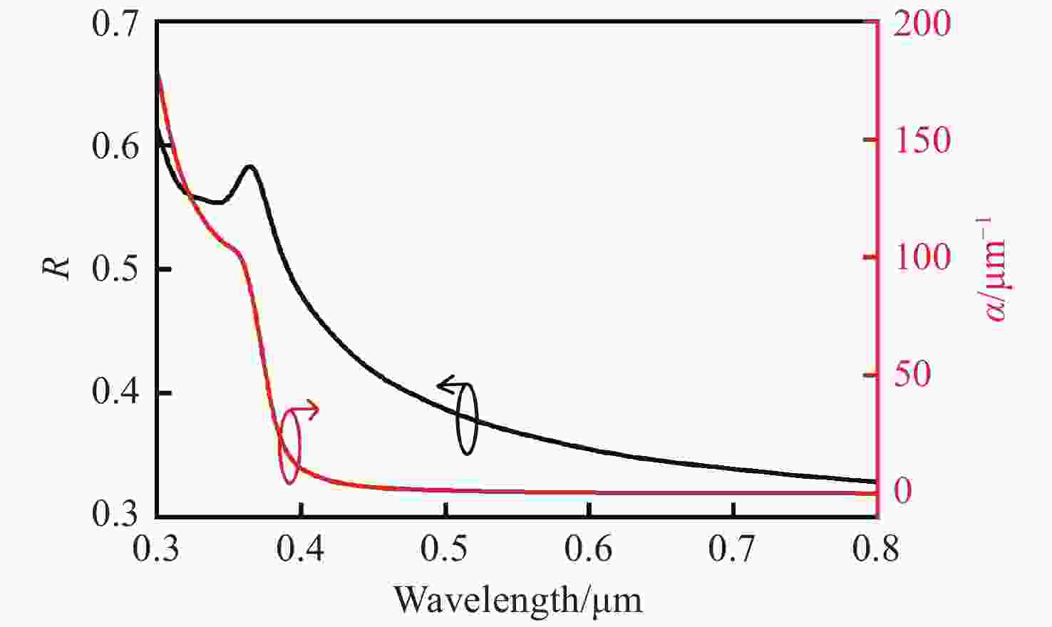
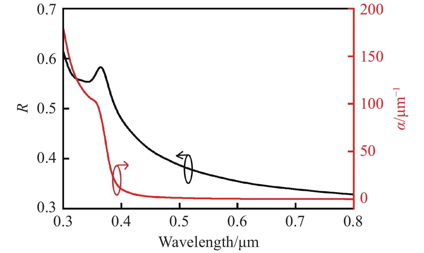
图 3 硅表面反射率及吸收系数随入射波长的变化情况
Figure 3. The surface reflectance and absorption coefficient of the silicon vary with different incident wavelengthes
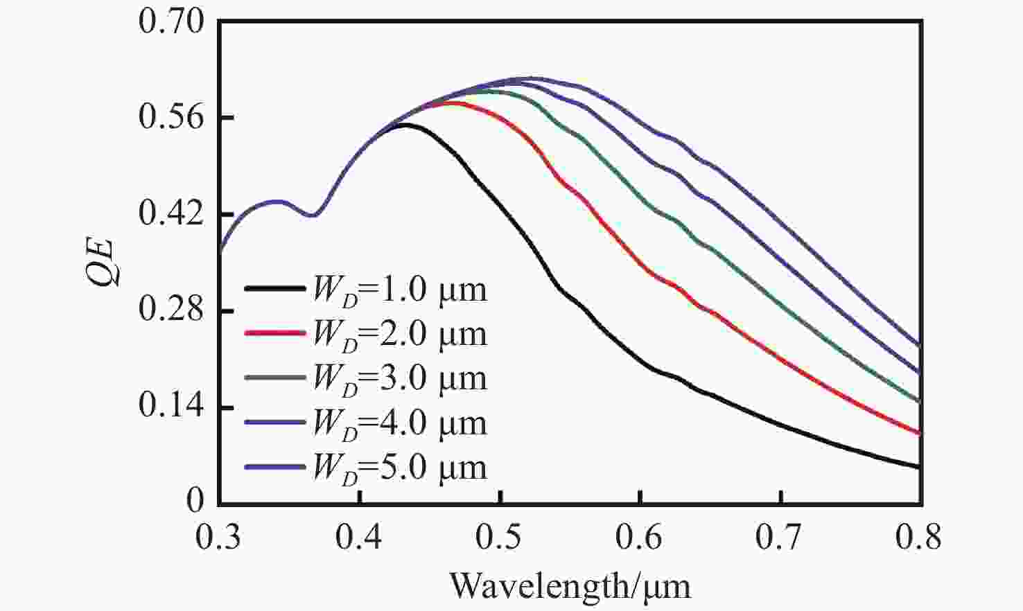
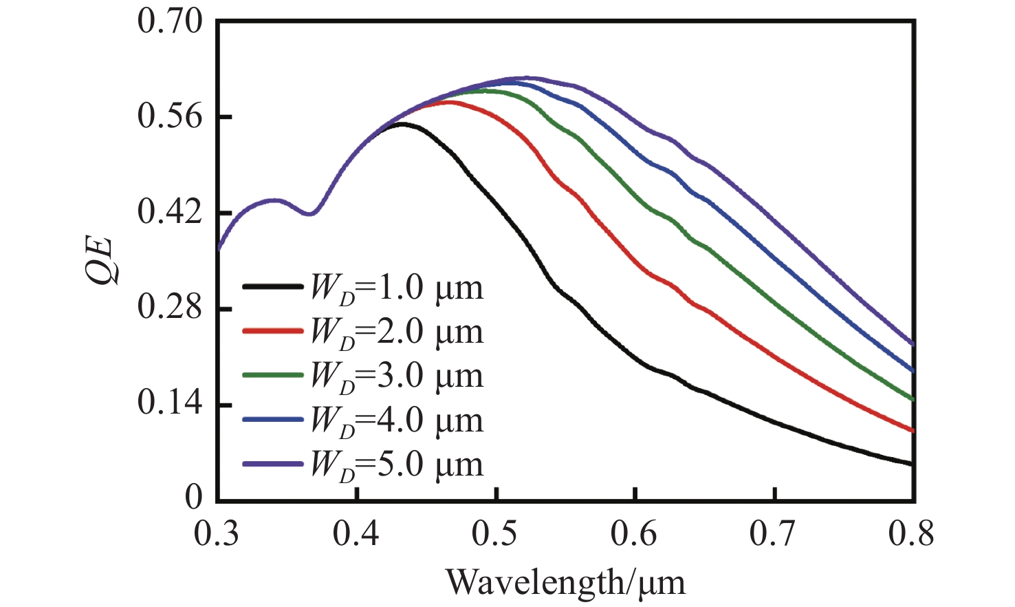
图 4 不同入射波长的量子效率与耗尽层厚度的关系
Figure 4. The relationship between quantum efficient and incident wavelength under different depletion layer thicknesses

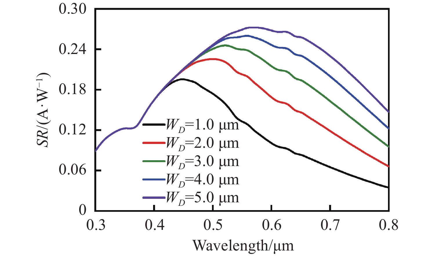
图 5 在不同耗尽层厚度下,光响应度与入射波长的关系
Figure 5. The relationship between spectral response and incident wavelength under different depletion layer thicknesses
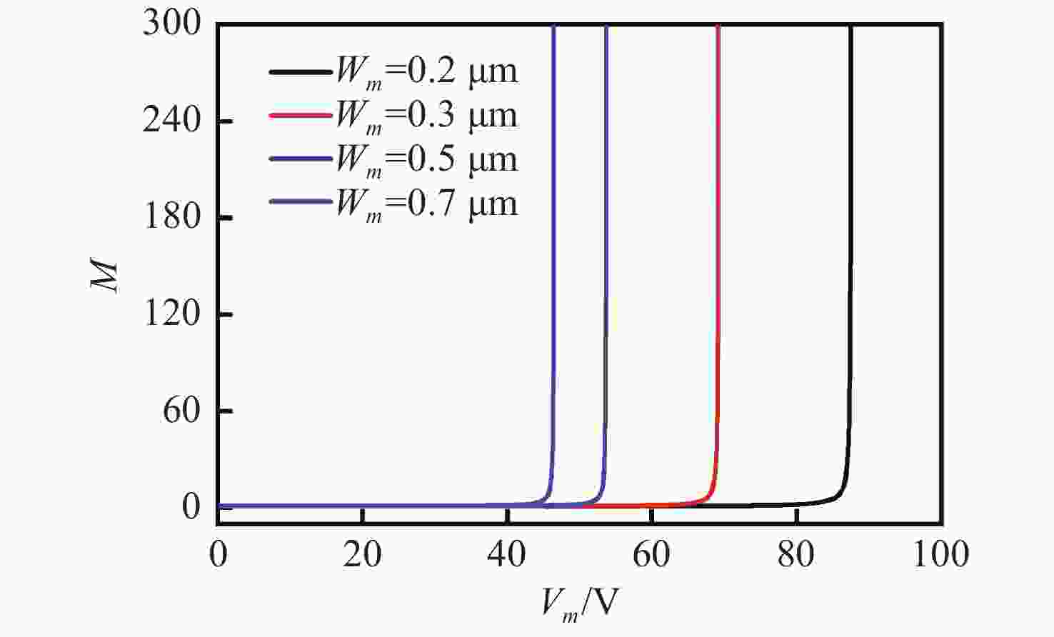
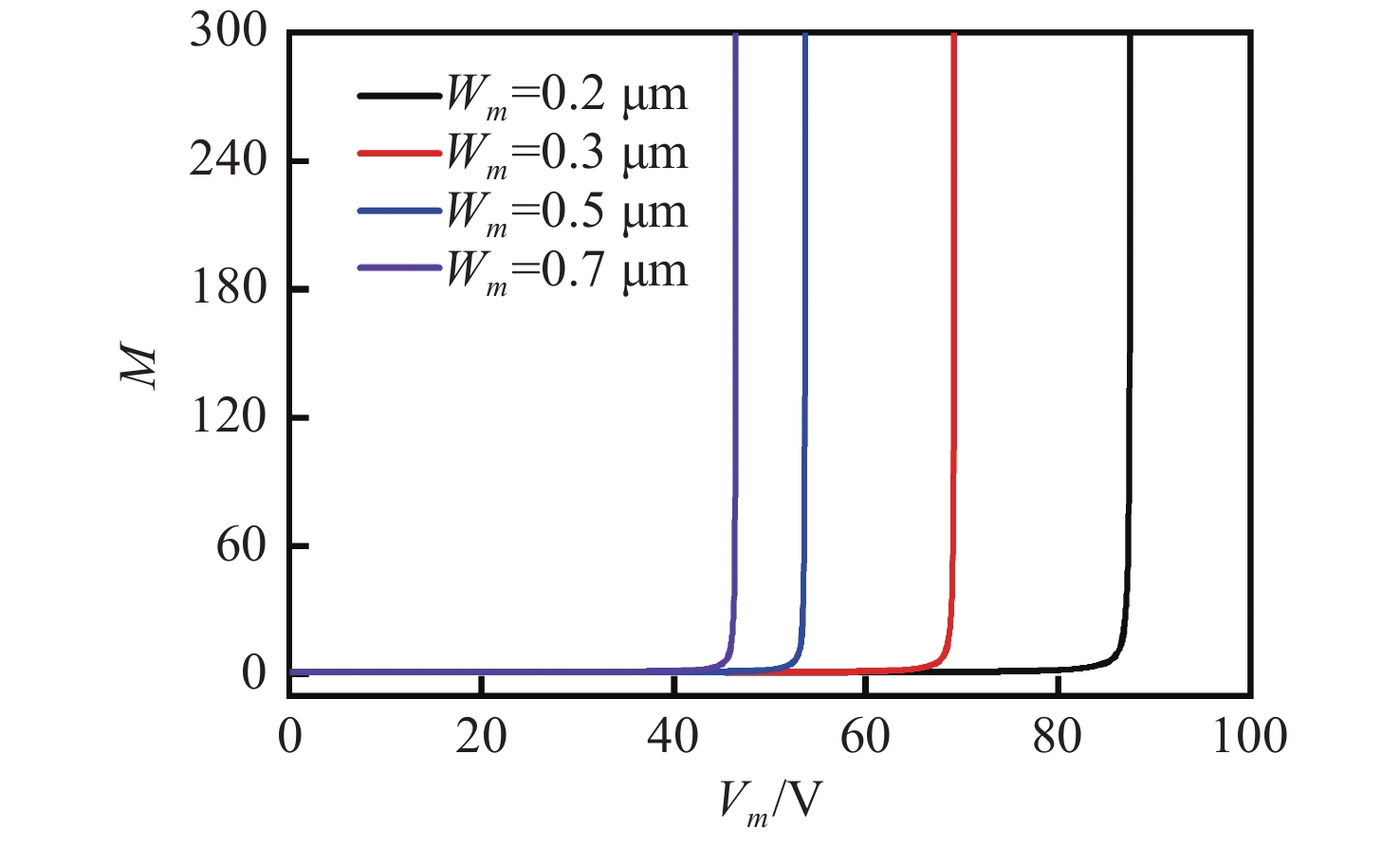
图 6 倍增层厚度与倍增系数M的关系
Figure 6. The relationship between the thickness of multiplication layer and multiplication factor M
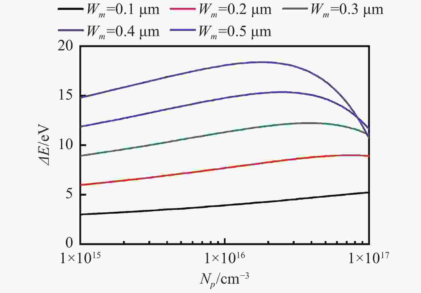
图 7 载流子获得能量ΔE与倍增层掺杂浓度的关系
Figure 7. Relationship between carrier energy ΔE and multiplication layer doping concentration
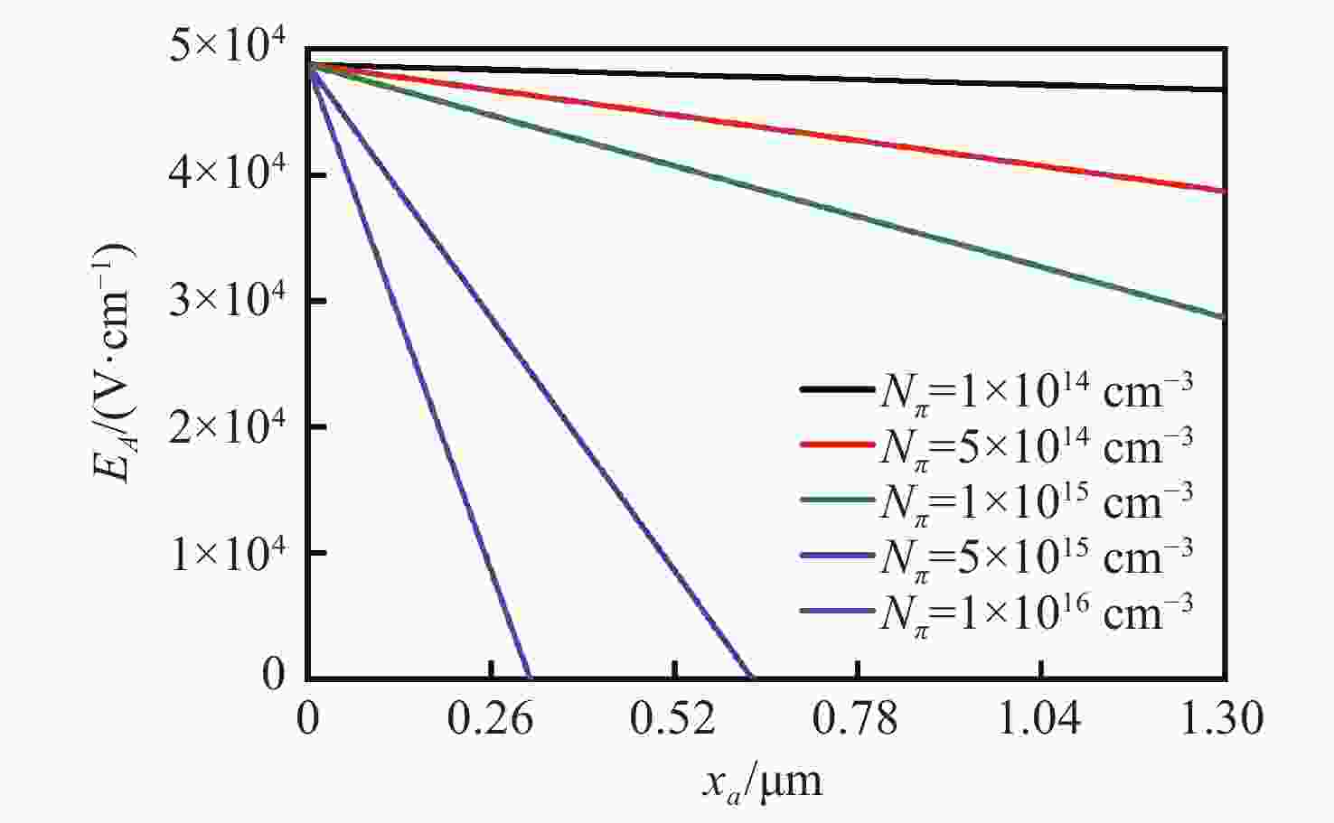
图 8 不同吸收层掺杂浓度下吸收层的场强分布
Figure 8. Field intensity distribution of the absorption layer under different doping concentrations
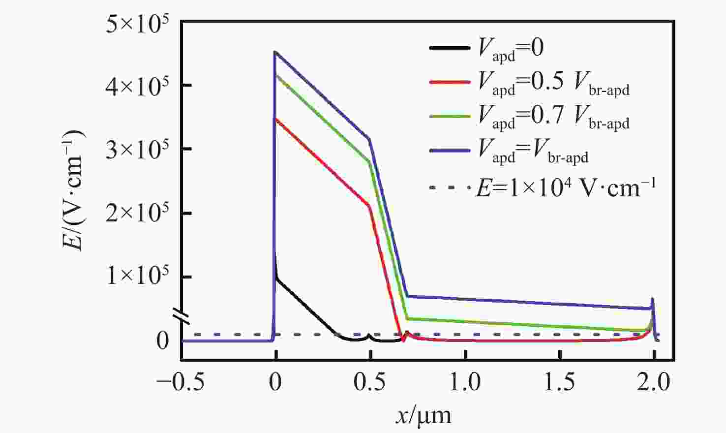
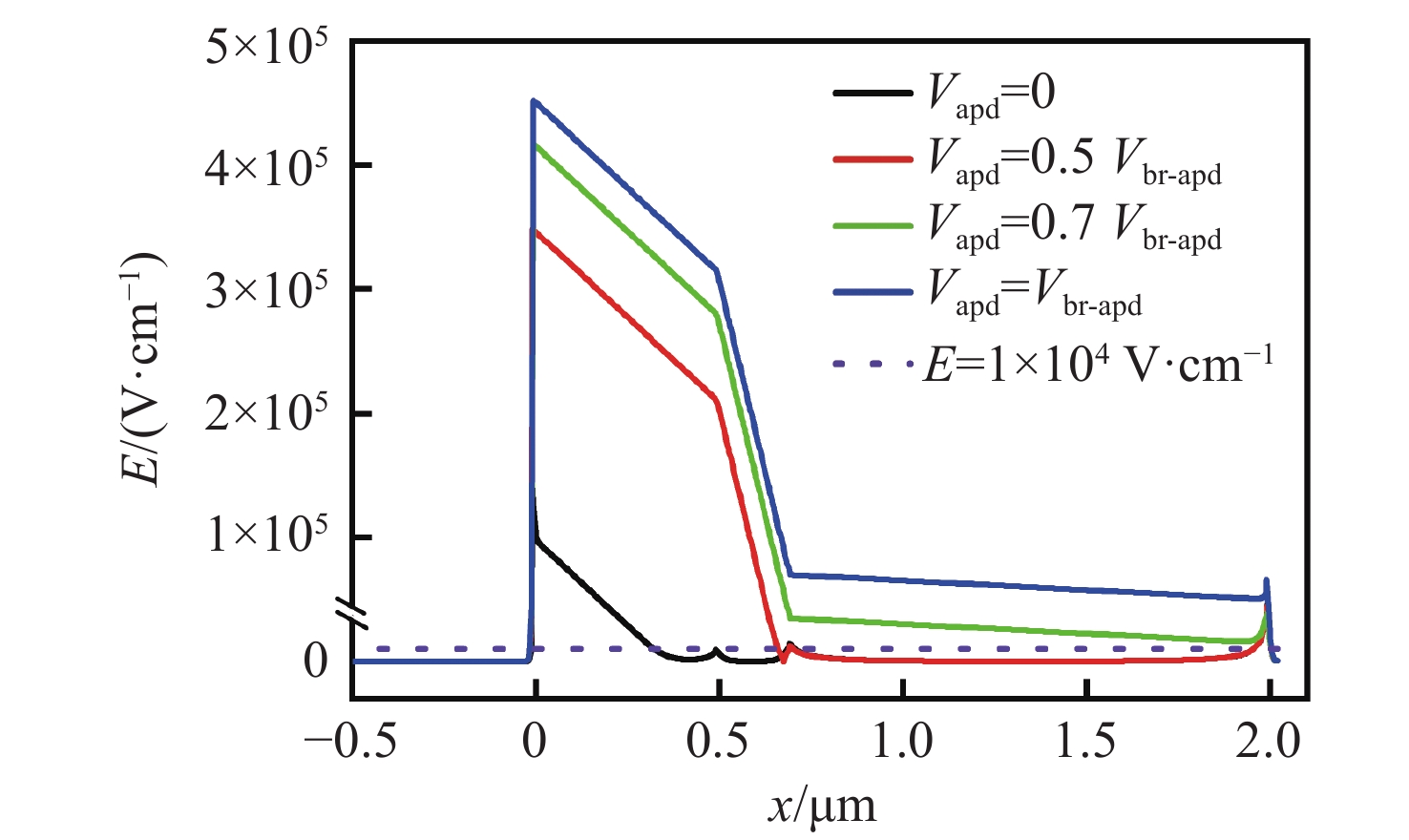
图 9 不同外加偏压下Si-APD的场强分布
Figure 9. The field strength distribution of Si-APD under different applied bias voltages
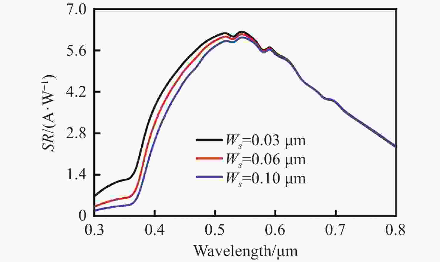
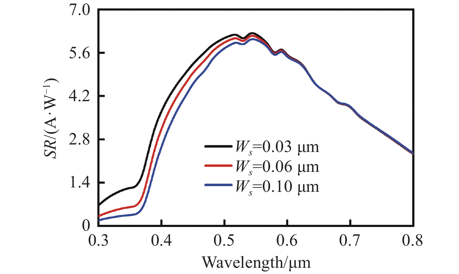
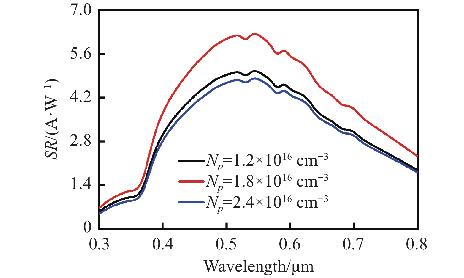
图 10 不同表面层厚度Si-APD的光谱响应曲线
Figure 10. Effect of thickness of surface layers of Si-APD on spectral responsivity
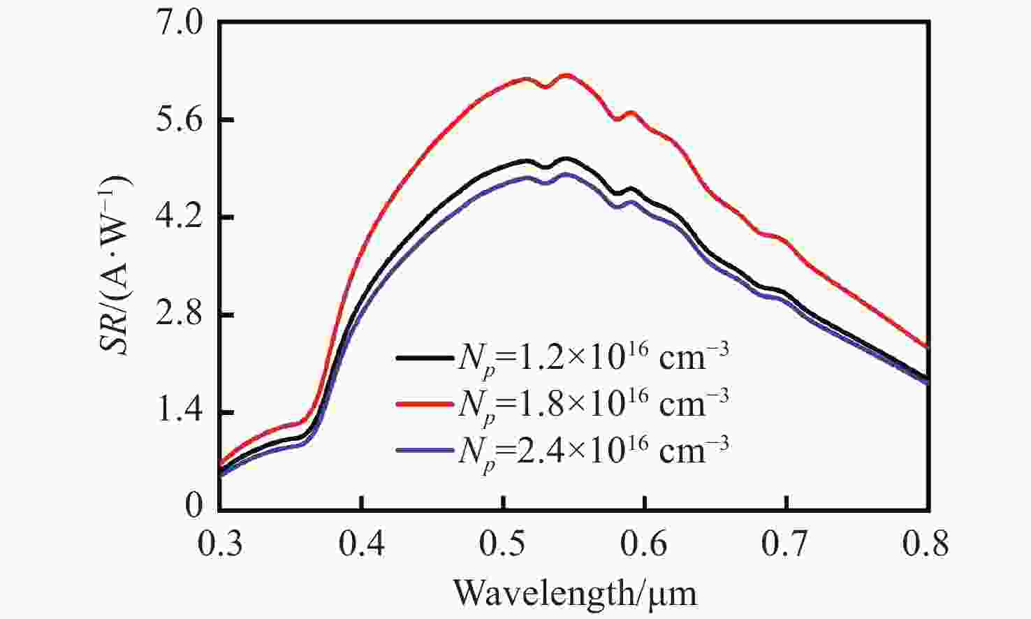
图 11 倍增层掺杂浓度对光响应度的影响
Figure 11. Effect of doping concentration of multiplication layer on spectral responsivity
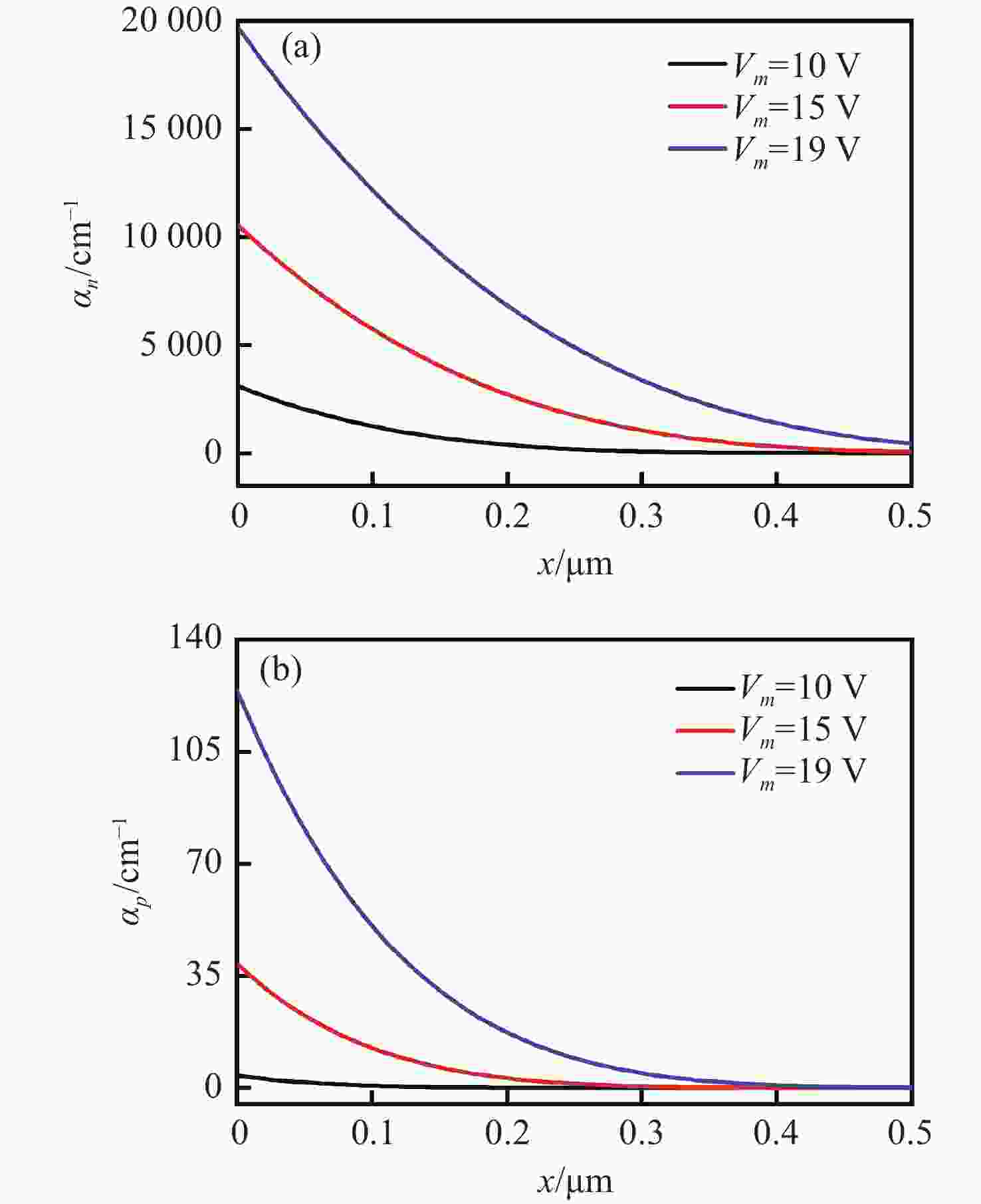
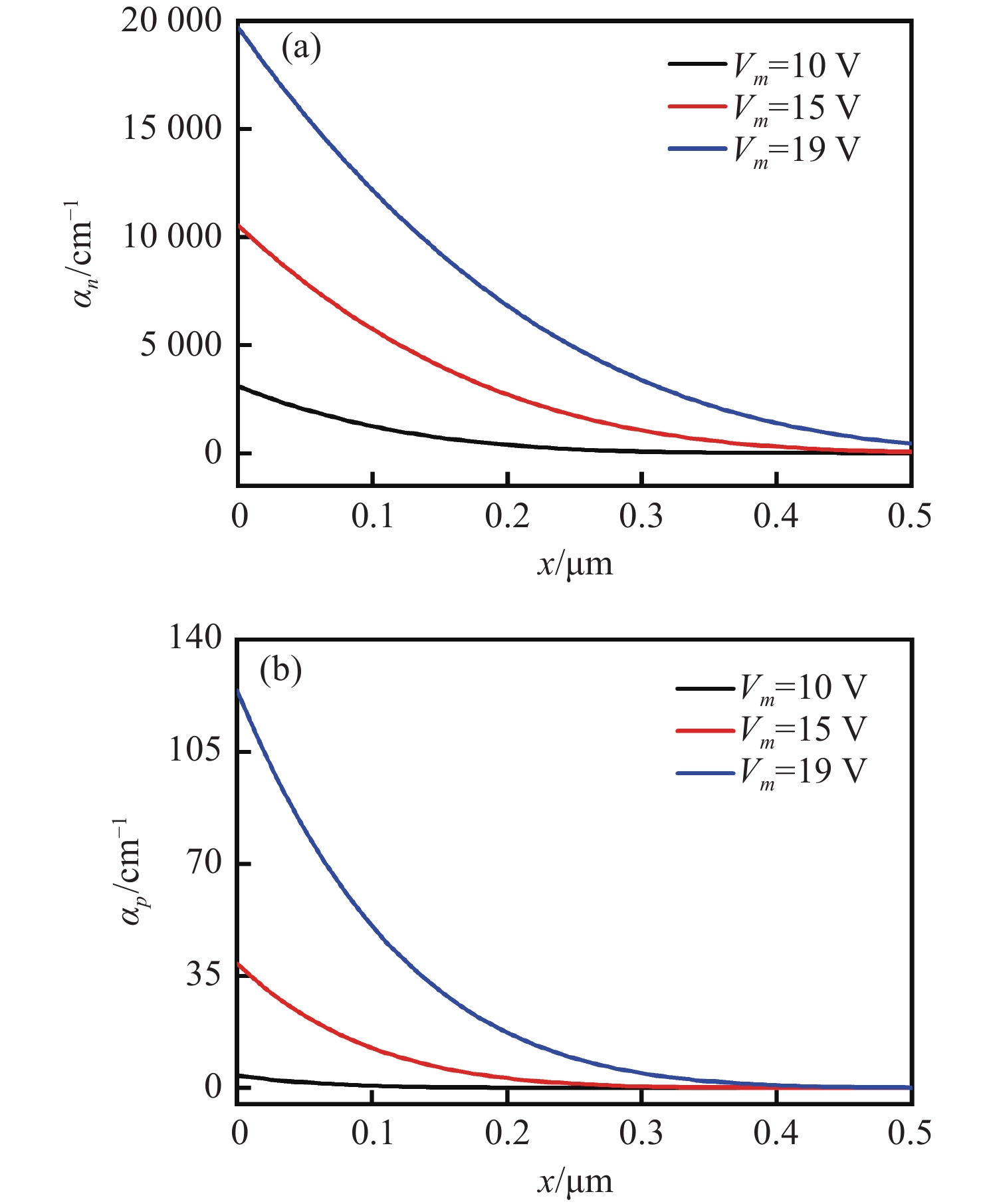
图 13 (a) 不同倍增层偏压下倍增层内电子离化系数; (b) 不同倍增层偏压下倍增层内空穴离化系数
Figure 13. (a) Electron ionization coefficients in the multiplication layer under different bias voltages; (b) hole ionization coefficients in the multiplication layer under different bias voltages.
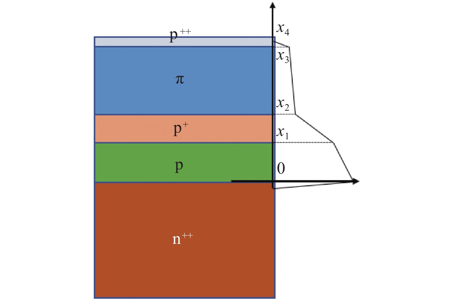
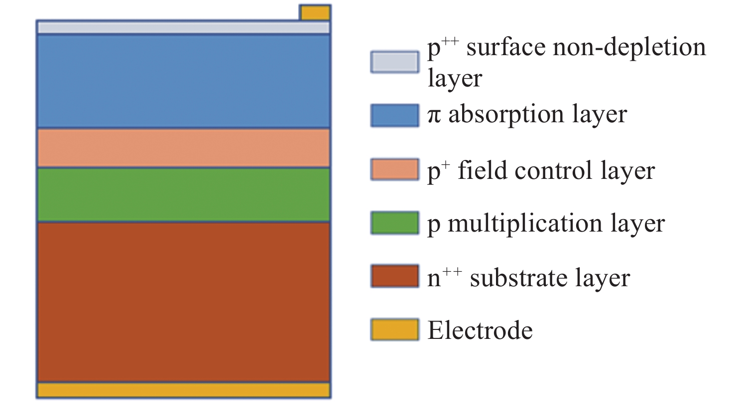
表 1 Parameters of Si-APD layers
Table 1. Parameters of Si-APD layers
Parameter Thickness/μm Doping type Impurity concentration/
(cm−3)Ws 0.06 p++ Np++= 1.0×10¹⁸ Wa 1.30 p- Nπ = 1.0×10¹⁵ Wc 0.20 p+ Np+ = 8.0×10¹⁶ Wm 0.50 p Np = 1.8×10¹⁶ Wsub 20.00 n++ Nn++ = 1.0×10¹⁹  下载: 导出CSV
表 2 Parameters of Si-APD layers
Table 2. Parameters of Si-APD layers
Parameter Thickness/μm Doping type Impurity concentration/
(cm−3)Ws 0.03 p++ Np++= 1.0×10¹⁸ Wa 1.30 p- Nπ = 1.0×10¹⁵ Wc 0.20 p+ Np+ = 8.0×10¹⁶ Wm 0.50 p Np = 1.8×10¹⁶ Wsub 20.00 n++ Nn++ = 1.0×10¹⁹
下载: 导出CSV
-
[1] DENG J ZH, CHENG X H. Visible light vehicle lamp signal transmission control device[J]. Optics and Precision Engineering, 2020, 28(12): 2710-2718. (in Chinese) doi: 10.37188/OPE.20202812.2710 [2] DONG B, TONG SH F, ZHANG P, et al. Design of a 20 m underwater wireless optical communication system based on blue LED[J]. Chinese Optics, 2021, 14(6): 1451-1458. (in Chinese) doi: 10.37188/CO.2020-0190 [3] LIU Y, CAI X P, LIN L, et al. Research on the fusion technology of LED visible optical communication network with Ethernet[J]. Optical Communication Technology, 2019, 43(1): 1-4. (in Chinese) [4] XU X Y, YUE D W. Orthogonal frequency division multiplexing modulation techniques in visible light communication[J]. Chinese Optics, 2021, 14(3): 516-527. (in Chinese) doi: 10.37188/CO.2020-0051 [5] ZHOU ZH, MIAO W N, LI Y, et al. Influence mechanism of GaN-LED's PN junction area on modulation bandwidth in visible light communication[J]. Optics and Precision Engineering, 2020, 28(7): 1494-1499. (in Chinese) doi: 10.37188/OPE.20202807.1494 [6] ZHOU Q CH, BAI Z L, LU L, et al. Remote phosphor technology for white LED applications: advances and prospects[J]. Chinese Optics, 2015, 8(3): 313-328. (in Chinese) doi: 10.3788/co.20150803.0313 [7] CHEN X B, MIN CH Y. Wireless communication that we can see——visible light communication[J]. Physics, 2020, 49(10): 688-696. (in Chinese) doi: 10.7693/wl20201005 [8] GAO X M. Study on silicon based nitride homologous optoelectronic integrated chip for visible light communication[D]. Nanjing: Nanjing University of Posts and Telecommunications, 2018. (in Chinese) [9] ZIMMERMANN R, BRAUN F, ACHTNICH T, et al. Silicon photomultipliers for improved detection of low light levels in miniature near-infrared spectroscopy instruments[J]. Biomedical Optics Express, 2013, 4(5): 659-666. doi: 10.1364/BOE.4.000659 [10] WEI J T. The structure design and research of new type APD based on silicon and germanium[D]. Harbin: Harbin Engineering University, 2016. (in Chinese) [11] ZHU X X, GE Y, LI J J, et al. Research progress of quantum dot enhanced silicon-based photodetectors[J]. Chinese Optics, 2020, 13(1): 62-74. (in Chinese) doi: 10.3788/co.20201301.0062 [12] WANG Y M, SHU H W, HAN X Y. High-precision silicon-based integrated optical temperature sensor[J]. Chinese Optics, 2021, 14(6): 1355-1361. (in Chinese) doi: 10.37188/CO.2021-0054 [13] MOLL J L, VAN OVERSTRAETEN R. Charge multiplication in silicon p-n junctions[J]. Solid-State Electronics, 1963, 6(2): 147-157. doi: 10.1016/0038-1101(63)90009-1 [14] PEPIN C M, DAUTET H, BERGERON M, et al.. New UV-enhanced, ultra-low noise silicon avalanche photodiode for radiation detection and medical imaging[C]. IEEE Nuclear Science Symposuim & Medical Imaging Conference, IEEE, 2010: 1740-1746. [15] OTHMAN M A, YASIN N Y M, ARSHAD T S M, et al.. Variable intrinsic region in CMOS PIN photodiode for I–V characteristic analysis[C]. Proceedings of the 1st International Conference on Communication and Computer Engineering, Springer, 2015: 95-101. [16] WANG X D. Optimization of the enhancement of the Si-based APD for near-ultraviolet detection through structural design[D]. Harbin: Harbin Institute of Technology, 2015. (in Chinese) [17] HUO L ZH, TAN H SH, HE R, et al. Research of blue-violet enhanced silicon photomultiplier[J]. Laser &Optoelectronics Progress, 2015, 52(11): 110401. (in Chinese) [18] LU H H. Simulation study on silicon-based blue-light enhanced APD detector for visible light communication[D]. Guangzhou: Jinan University, 2019. (in Chinese) [19] SCHINKE C, PEEST P C, SCHMIDT J, et al. Uncertainty analysis for the coefficient of band-to-band absorption of crystalline silicon[J]. AIP Advances, 2015, 5(6): 067168. doi: 10.1063/1.4923379 [20] CHEN F. The enhancement of the APD for Blu-Ray detection in VLC[D]. Changchun: Changchun University of Science and Technology, 2018. (in Chinese) [21] WANG H B. Research on enhancement in blue-light properties of silicon based avalanche photodiode[D]. Beijing: University of Chinese Academy of Sciences (Changchun Institute of Optics, Precision Machinery and Physics, Chinese Academy of Sciences), 2020. (in Chinese) [22] SHI Y L, ZHU H X, YANG X Y, et al. InP-based free running mode single photon avalanche photodiode[J]. Infrared and Laser Engineering, 2020, 49(1): 0103005. (in Chinese) [23] LIU E K, ZHU D SH, LUO J SH. Physics of Semiconductors[M]. 7th ed. Beijing: Publishing House of Electronics Industry, 2017: 66-67. (in Chinese) [24] CHYNOWETH A G. Chapter 4 charge multiplication phenomena[J]. Semiconductors and Semimetals, 1968, 4: 263-325. [25] YANG M. The research of silicon avalanche photodiode single photon detector on space quantum communication[D]. Hefei: University of Science and Technology of China, 2019. (in Chinese) [26] LI Y. Theoretical and experimental study on avalanche photodiodes and optimization design[D]. Wuhan: Huazhong University of Science and Technology, 2017. (in Chinese) [27] SZE S M, NG K K. Physics of Semiconductor Devices[M]. GENG L, ZHANG R ZH, trans. 3rd ed. Xi'an: Xi'an Jiaotong University Press, 2008. (in Chinese) [28] WOODS M H, JOHNSON W C, LAMPERT M A. Use of a Schottky barrier to measure impact ionization coefficients in semiconductors[J]. Solid-State Electronics, 1973, 16(3): 381-394. doi: 10.1016/0038-1101(73)90013-0 [29] FOSSUM J G, MERTENS R P, LEE D S, et al. Carrier recombination and lifetime in highly doped silicon[J]. Solid-State Electronics, 1983, 26(6): 569-576. doi: 10.1016/0038-1101(83)90173-9 [30] OLDHAM W G, SAMUELSON R R, ANTOGNETTI P. Triggering phenomena in avalanche diodes[J]. IEEE Transactions on Electron Devices, 1972, 19(9): 1056-1060. doi: 10.1109/T-ED.1972.17544 [31] GAO D, ZHANG J, WANG F, et al. Design and simulation of ultra-thin and high-efficiency silicon-based trichromatic PIN photodiode arrays for visible light communication[J]. Optics Communications, 2020, 475: 126296. doi: 10.1016/j.optcom.2020.126296 [32] VAN OVERSTRAETEN R, DE MAN H. Measurement of the ionization rates in diffused silicon p-n junctions[J]. Solid-State Electronics, 1970, 13(5): 583-608. doi: 10.1016/0038-1101(70)90139-5 [33] SELBERHERR S. Analysis and Simulation of Semiconductor Devices[M]. Vienna: Springer, 1984. [34] HALL R N. Electron-hole recombination in germanium[J]. Physical Review, 1952, 87(2): 387. [35] SHOCKLEY W, READ JR W T. Statistics of the recombinations of holes and electrons[J]. Physical Review, 1952, 87(5): 835-842. doi: 10.1103/PhysRev.87.835 [36] ARORA N D, HAUSER J R, ROULSTON D J. Electron and hole mobilities in silicon as a function of concentration and temperature[J]. IEEE Transactions on Electron Devices, 1982, 29(2): 292-295. doi: 10.1109/T-ED.1982.20698 [37] CAUGHEY D M, THOMAS R E. Carrier mobilities in silicon empirically related to doping and field[J]. Proceedings of the IEEE, 1967, 55(12): 2192-2193. doi: 10.1109/PROC.1967.6123 [38] MASETTI G, SEVERI M, SOLMI S. Modeling of carrier mobility against carrier concentration in arsenic-, phosphorus-, and boron-doped silicon[J]. IEEE Transactions on Electron Devices, 1983, 30(7): 764-769. doi: 10.1109/T-ED.1983.21207 [39] FORREST S. Performance of InxGa1-xAsyP1-yphotodiodes with dark current limited by diffusion, generation recombination, and tunneling[J]. IEEE Journal of Quantum Electronics, 1981, 17(2): 217-226. doi: 10.1109/JQE.1981.1071060 [40] GU H Q. The study of avalanche gain and structural parameter optimization in Si based micro-pixel APD[D]. Harbin: Harbin Institute of Technology, 2012. (in Chinese) -

 下载:
下载:


计量
- 文章访问数: 1066
- HTML全文浏览量: 642
- PDF下载量: 200
- 被引次数: 0
