


Structural optimization and performance testing of gold microarray electrode fabricated by DMD lithography and electrodeposition
doi: 10.37188/CO.2021-0109
-
摘要: 为提高微阵列电极 (Microarray electrodes, MAE) 的检测效率,降低生产成本,提出了一种将数字微镜器件 (DMD) 无掩模投影光刻与电化学沉积相结合的技术。首先,利用光刻系统压电平台 (PZS) 的高分辨率运动和DMD生成图案的灵活性等优点,制备了用户可自定义的微结构阵列,接着,通过电化学沉积获得Au导电层,实现了均匀的Au微阵列电极 (Au/MAE) 的制备。然后通过循环伏安法,比较了不同结构的Au/MAE的电化学性能,获得了优化的结构参数。最后,研究了优化后的Au/MAE对于不同浓度和pH值的葡萄糖的电流响应,并通过计时电流法对Au/MAE检测葡萄糖的抗干扰能力进行了测试。电化学分析表明,这种简单的Au/MAE对葡萄糖的电化学检测具有显著的安培响应和较强的抗干扰能力,其灵敏度为101 μA·cm−2·mM−1。这种微阵列电极的制备方法,具有分辨率高、一致性高、工艺简单、成本低的优点,为生物传感阵列的制造提供了切实可行的操作方案。Abstract: In order to improve the detection efficiency of Micro Array Electrodes (MAE) and reduce the production cost, a technology combining Digital Micromirror Device (DMD) maskless projection lithography with electrochemical deposition was proposed. Firstly, a user-defined micro array was fabricated by using the advantages of lithography system such as high-resolution PZS motion and imaging flexibility of DMD. And a uniform Au microarray electrode (Au/MAE) was fabricated after obtaining an Au conducting layer by electrodeposition. Then, the electrochemical properties of Au/MAE with different structures were compared by cyclic voltammetry, and the optimized structural parameters were obtained. Finally, the current response of optimized Au/MAE to the glucose with different concentrations and pH values was studied, and the anti-interference of Au/MAE in glucose detection was tested by chronoamperometry. The electrochemical analysis shows that the simple Au/MAE has a significant amperometric response, a strong anti-interference ability and a sensitivity of 101 μA·cm−2·mM−1 in the electrochemical detection of glucose. This method has the advantages of high resolution, high consistency, simple process and low cost, which provides a feasible operation scheme for the fabrication of biosensor array.
-
Key words:
- DMD lithography /
- electrochemical deposition /
- microstructure array /
- electrode
-
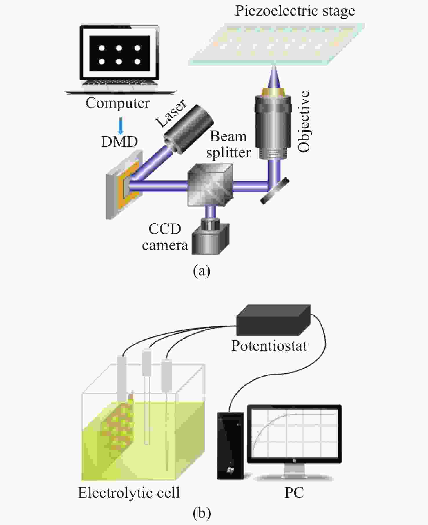
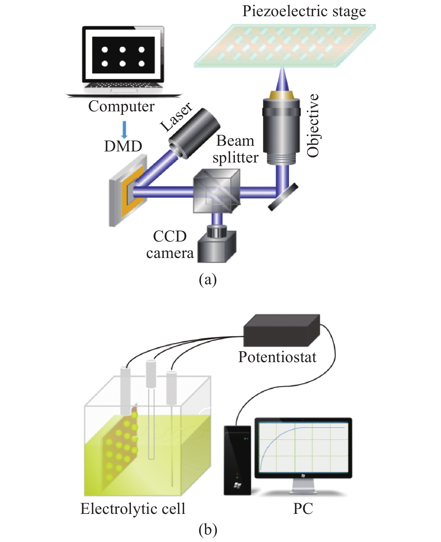
图 1 (a) 基于DMD的无掩模投影光刻系统示意图;(b) 电化学沉积的实验装置图
Figure 1. (a) Schematic diagram of maskless projection lithography system based on DMD and (b) experimental setup of electrochemical deposition
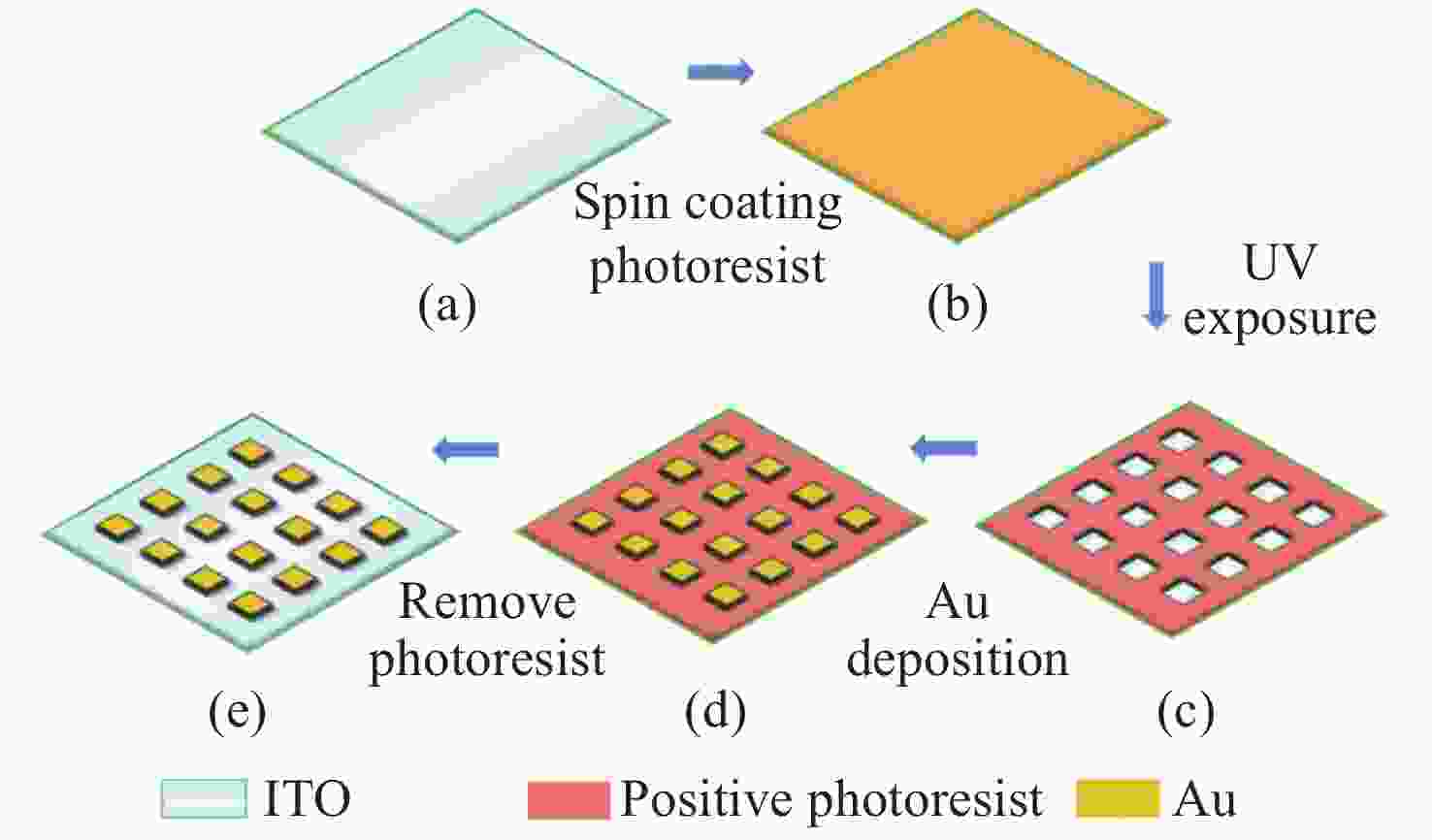
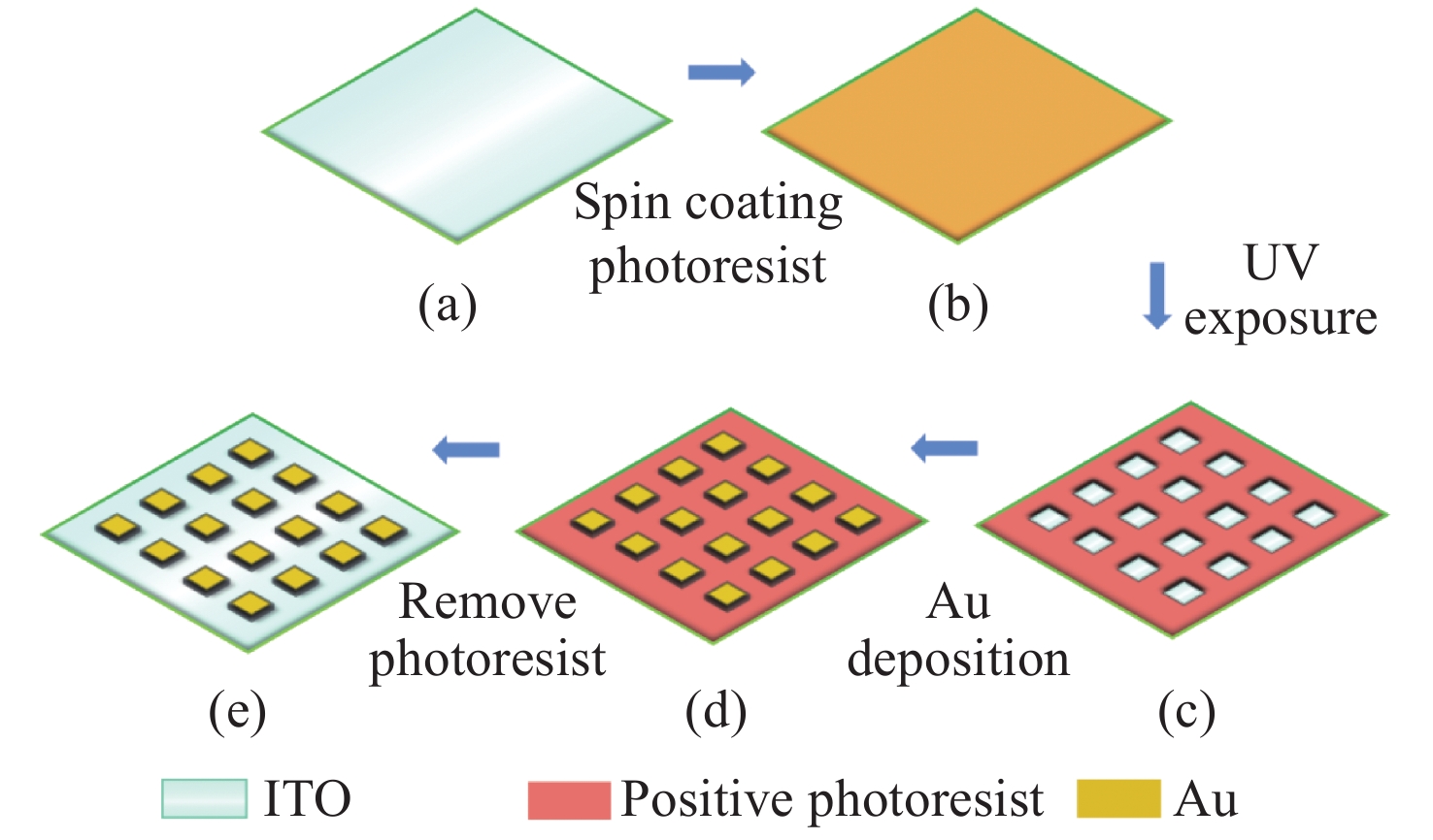
图 2 Au/MAE的制备流程图。 (a) 基片预处理;(b) 旋涂光刻胶和前烘;(c) 曝光并显影;(d) 电化学沉积Au纳米层;(e) 去除光刻胶
Figure 2. Flow chart of Au/MAE preparation process. (a) Substrate pretreatment; (b) photoresist spin-coating and pre drying; (c) exposure and development; (d) electrochemical deposition of Au nano layer; (e) photoresist removal
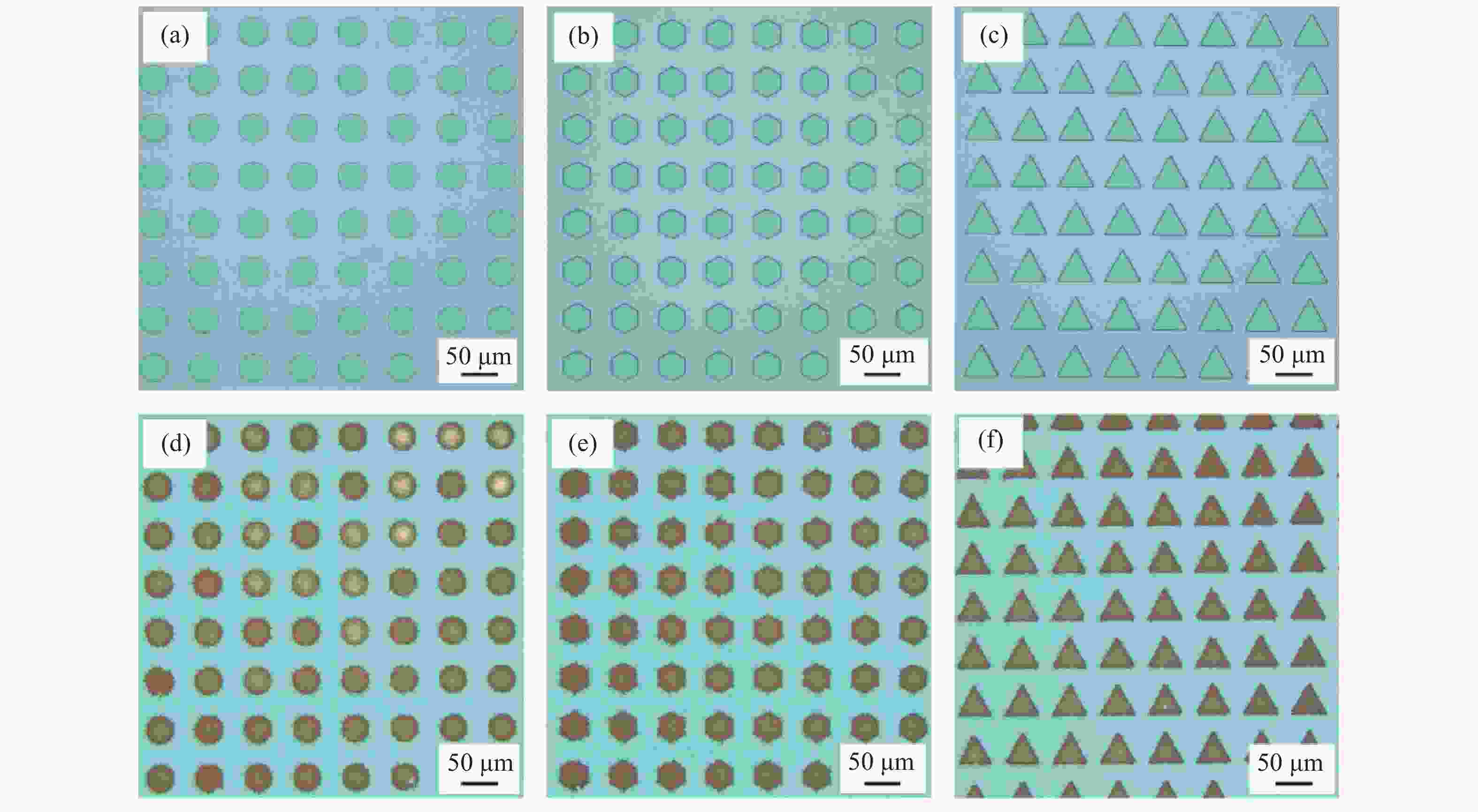
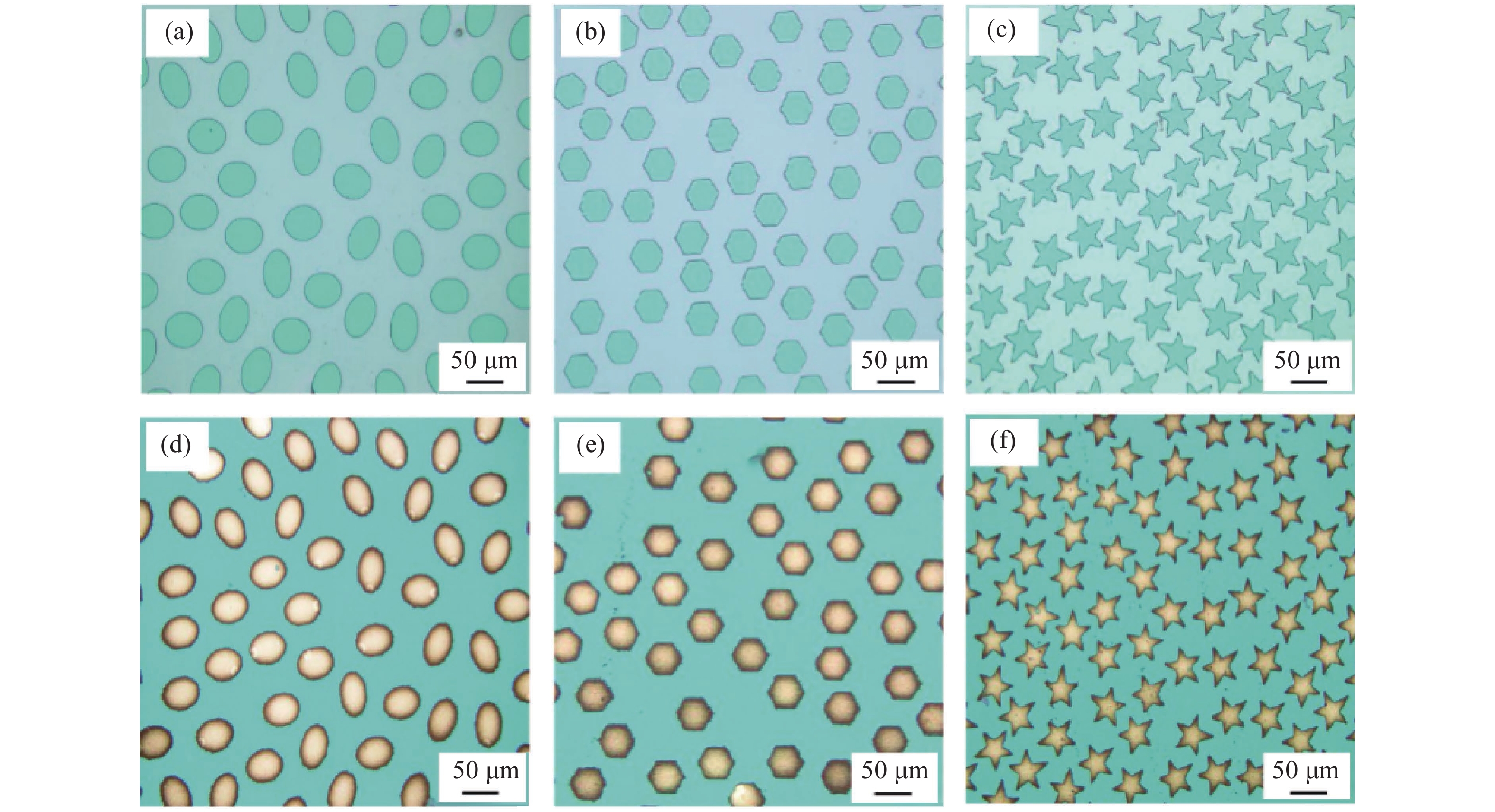
图 3 周期性结构测试结果。圆形 ( (a) 和 (d) ) ;六边形 ( (b) 和 (e) ) 以及三角形 ( (c) 和 (f) ) 的MAE和Au/MAE在光学显微镜下的实际曝光和电沉积结果
Figure 3. Results of periodic structures. The actual exposure and electrodeposition results of MAE and Au/MAE structures of circular ((a) and (d)); hexagonal ((b) and (e))and triangular ((c) and (f)) under optical microscope
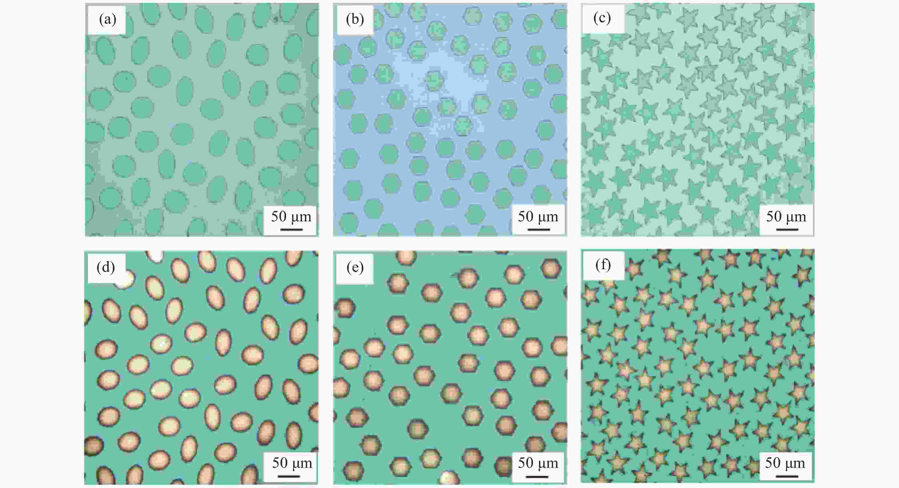
图 4 非周期性结构结果。椭圆形((a)和(d));六边形((b)和(e))以及五角星((c)和(f))的MAE和Au/MAE在光学显微镜下的实际曝光和电沉积结果
Figure 4. Aperiodic structures results. The actual exposure and electrodeposition results of MAE and Au/MAE of elliptical ((a) and (d));hexagonal ((b) and (e)) and five-pointed ((c) and (f)) under optical microscope
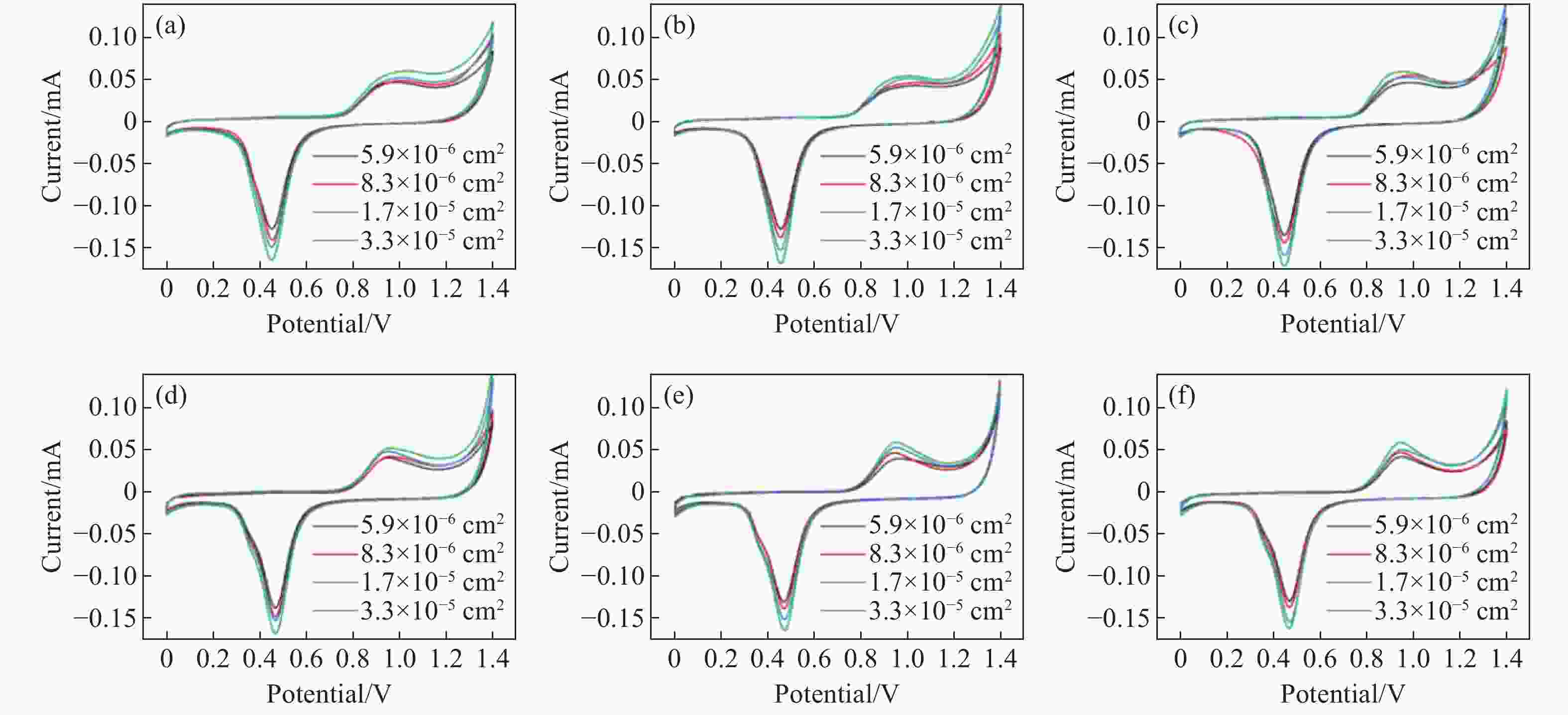
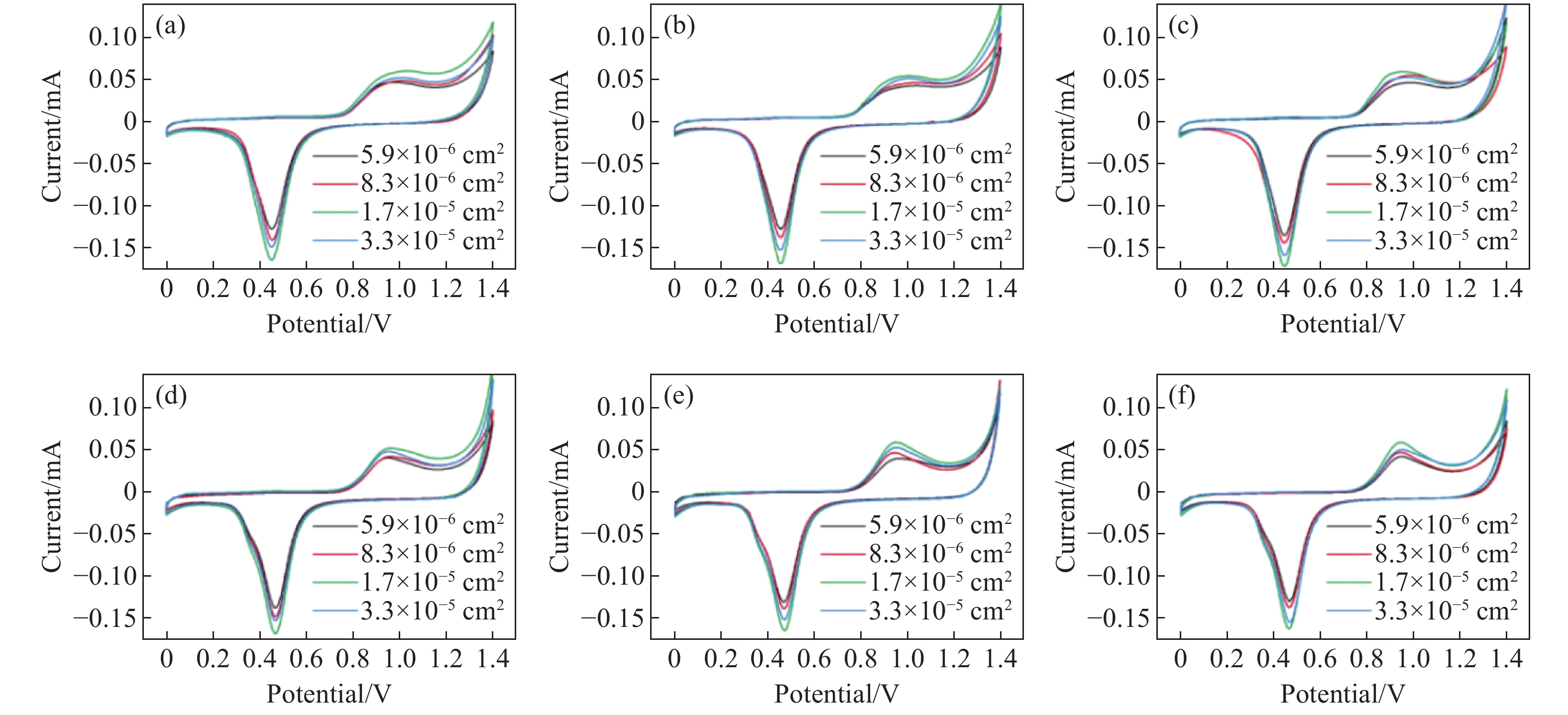
图 5 总表面积不变,单元表面积对氧化还原峰电流的影响,周期性排列的(a)圆形;(b)六边形;(c)三角形以及非周期性排列的(d)椭圆;(e)六边形;(f)五角星结构的Au/MAE的CV图
Figure 5. Effect of cell surface area on REDOX peak current under the same total surface area. CV diagrams of (a) circular; (b) hexagonal and (c) triangular Au/MAE structures with periodic arrangement and of (d) elliptical; (e) hexagonal and (f) five-pointed Au/MAE structures with aperiodic arrangement
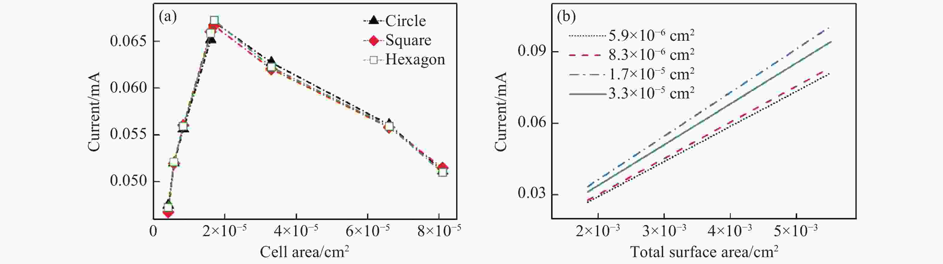
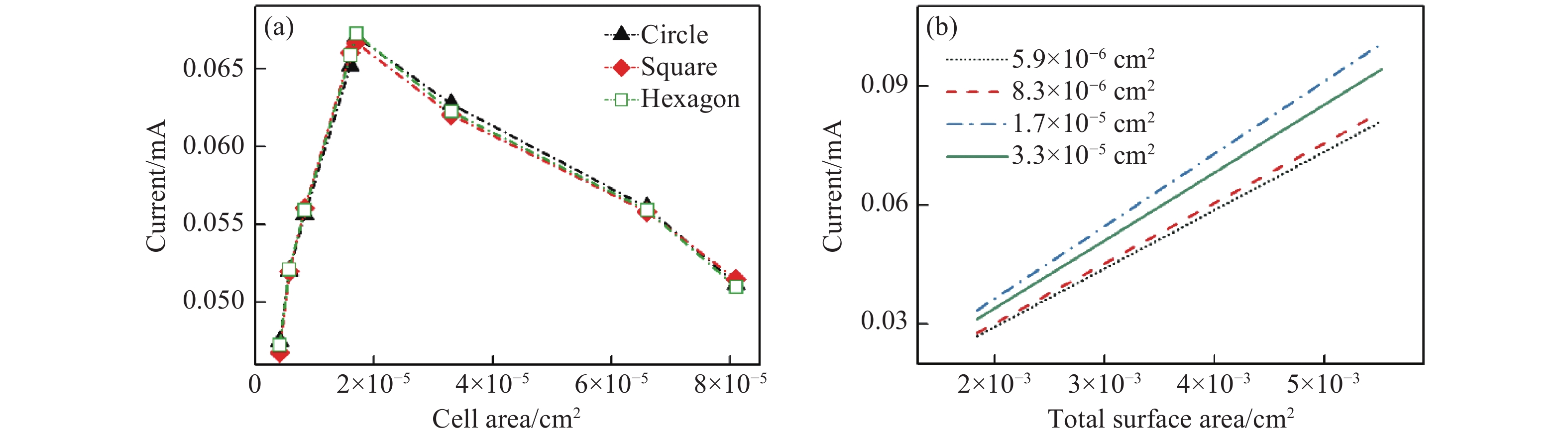
图 6 (a) 总表面积一定时,氧化峰电流值与电极单元表面积的关系;(b) 氧化峰电流值与电极的总表面
Figure 6. (a) Relationship between oxidation peak current and electrode cell surface area when total surface area is constant; (b) relationship between oxidation peak current and total electrode surface area
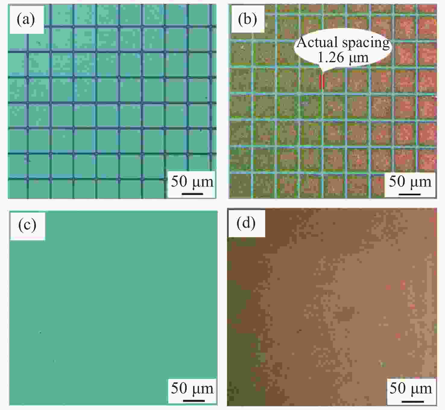
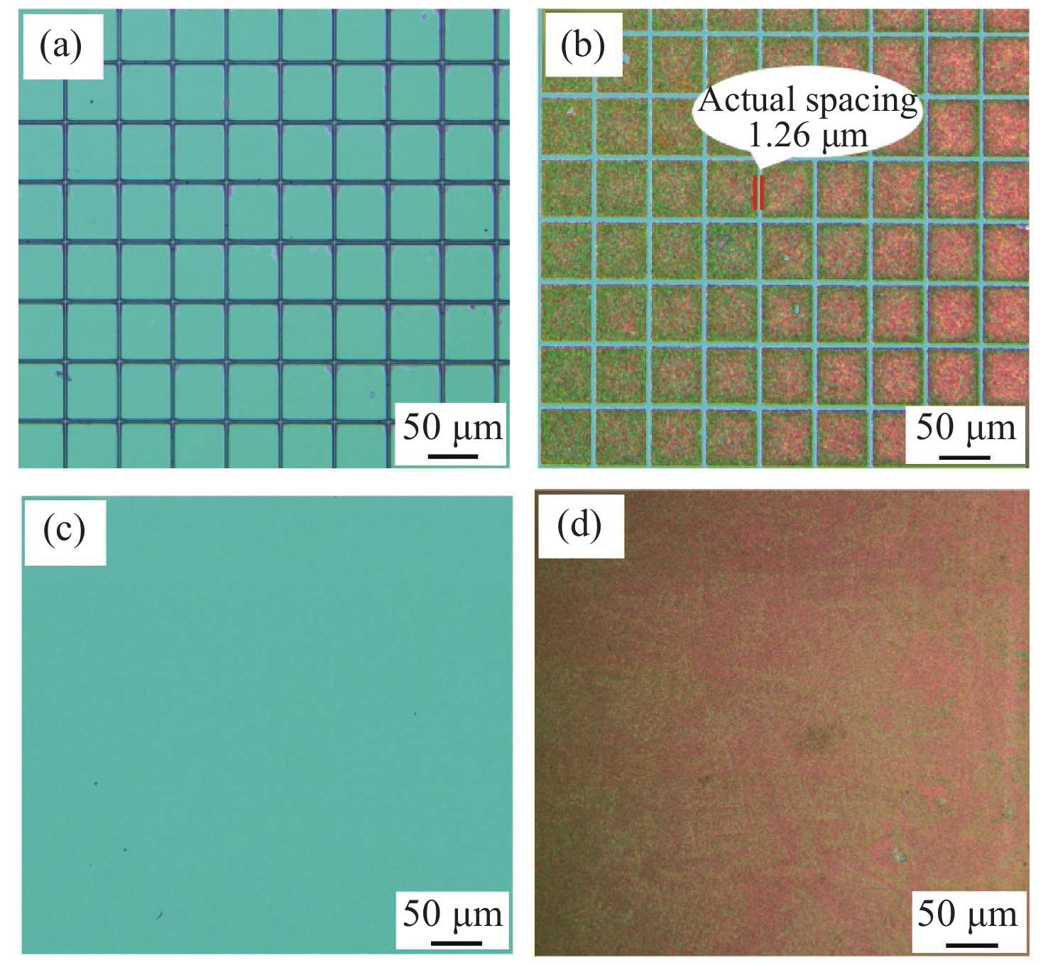
图 7 (a) 密集排列的MAE的显微镜图像;(b) 电沉积后的Au/MAE的光学显微镜图;(c)全部曝光后的显微镜图像;(d)电沉积后的单个Au电极光学显微镜图
Figure 7. (a) Microscope image of the MAE with the most densely arranged cells; (b) microscope image of Au/MAE after electrodeposition; (c) microscope image obtained after full exposure; (d) microscope image of single Au electrode after electrodeposition
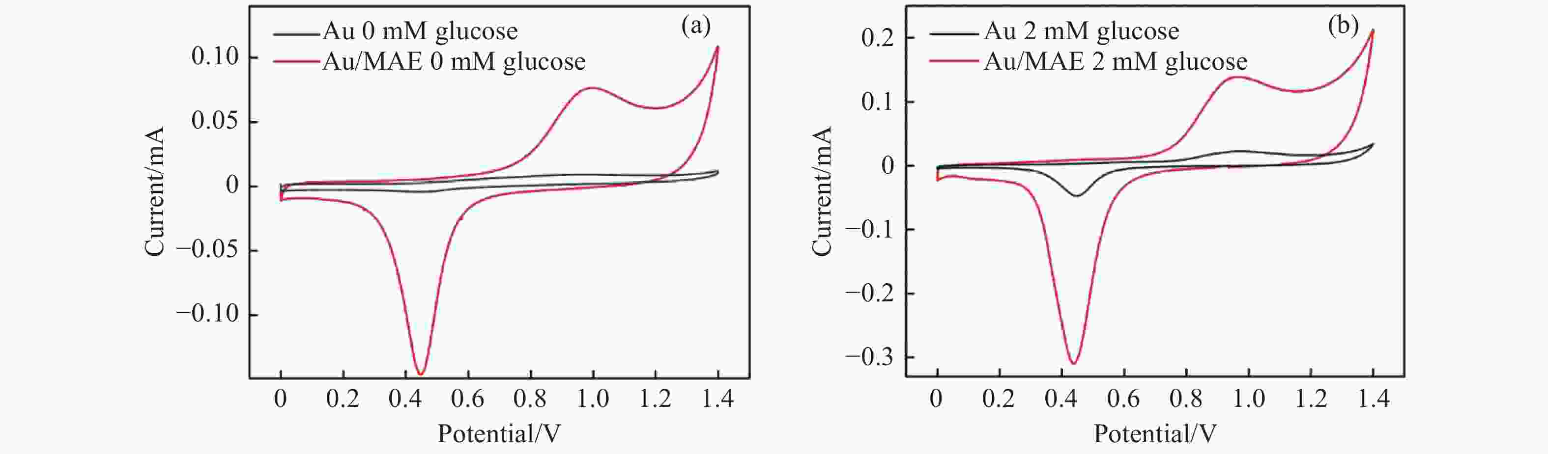
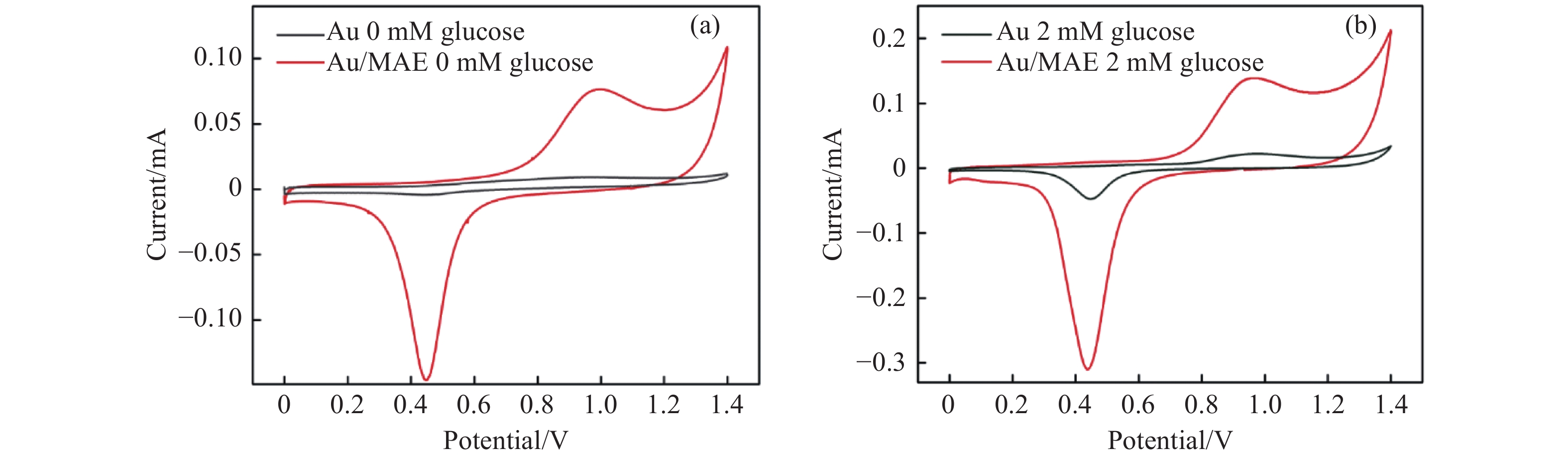
图 8 Au电极(a)与Au/MAE电极(b)电化学性能比较
Figure 8. Comparison of electrochemical performance between Au electrode (a) and Au/MAE (b)
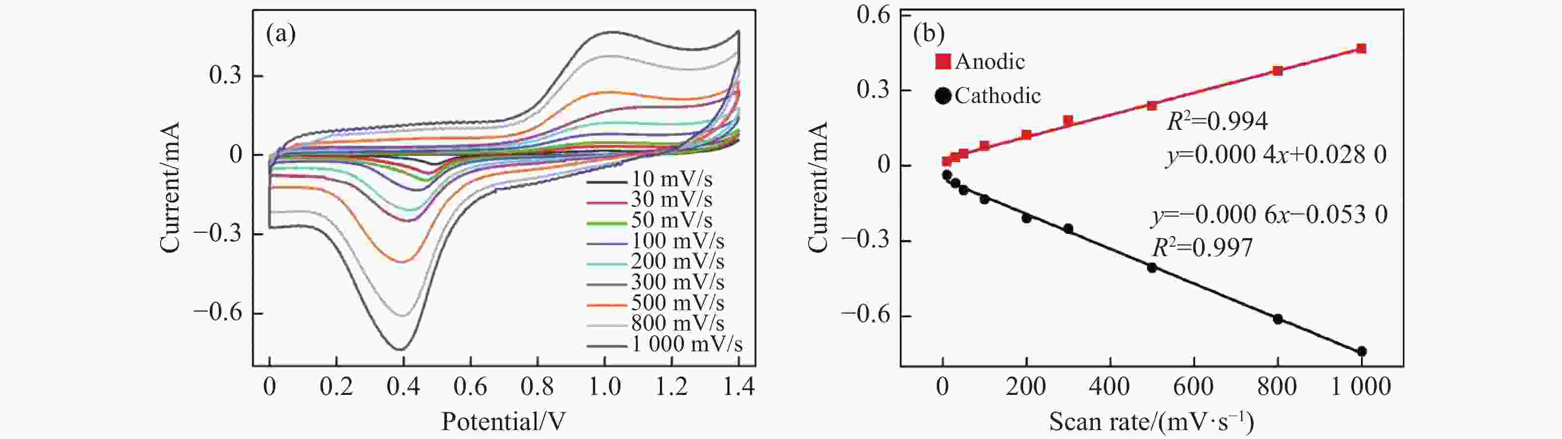
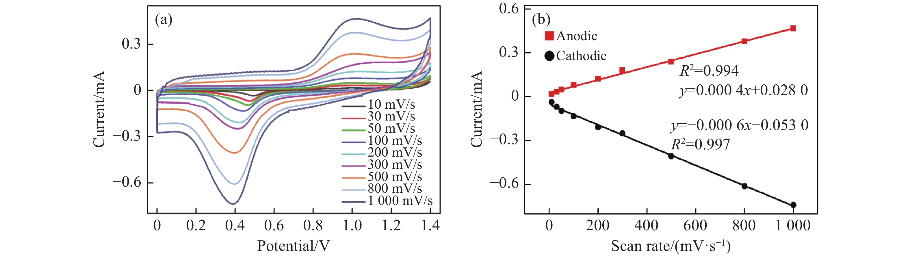
图 9 Au/MAE在含有1 mM葡萄糖的0.1 mM PBS(pH 7.0)缓冲溶液中, (a)不同扫描速度下 (10−1000 mV/s) 的CV图以及(b)不同扫描速率下的阳极和阴极峰值电流拟合图
Figure 9. For Au/MAE (glucose concentration: 1 mM) in 0.1 mM PBS (pH 7.0) buffer solution, (a) CV diagram at different scanning rates (10−1000 mV/s); (b) fitting diagram of anodic and cathodic peak currents at different scanning rates

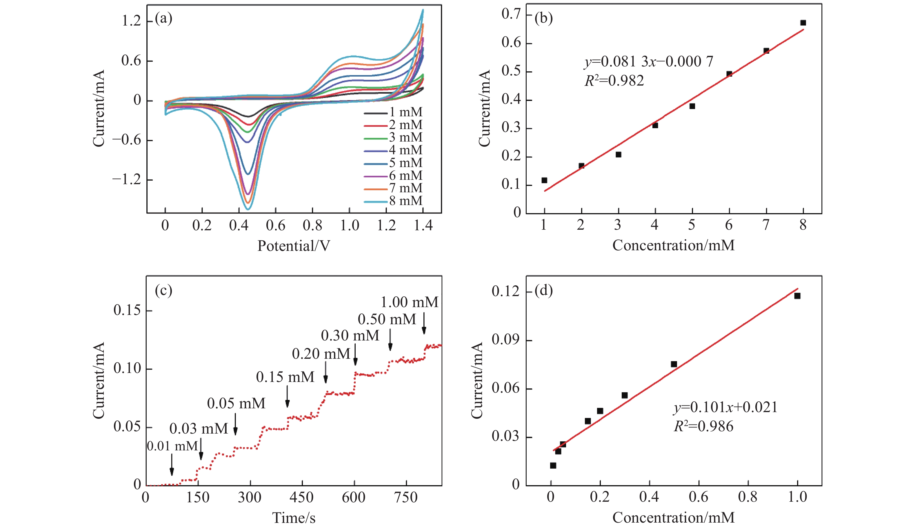
图 10 0.1 mM PBS (pH 7.0) 条件下,(a) 葡萄糖浓度不同时Au/MAE的循环伏安图(扫描速率100 mV/s)及(b) 相应的校准曲线;(c) Au/MAE在0.5 V电压下,0.1 mM PBS中连续加入葡萄糖时的安培响应; (d) 对应的拟合曲线
Figure 10. (a) Cyclic voltammograms of Au/MAE electrode at different glucose concentrations in 0.1 mM PBS (pH 7.0) (scanning rate: 100 mV/s) and (b) the corresponding calibration curve; (c) amperometric response of Au/MAE electrode to the continuous addition of glucose to 0.1 mM PBS at the voltage of 0.5 V and (d) the corresponding fitting curve
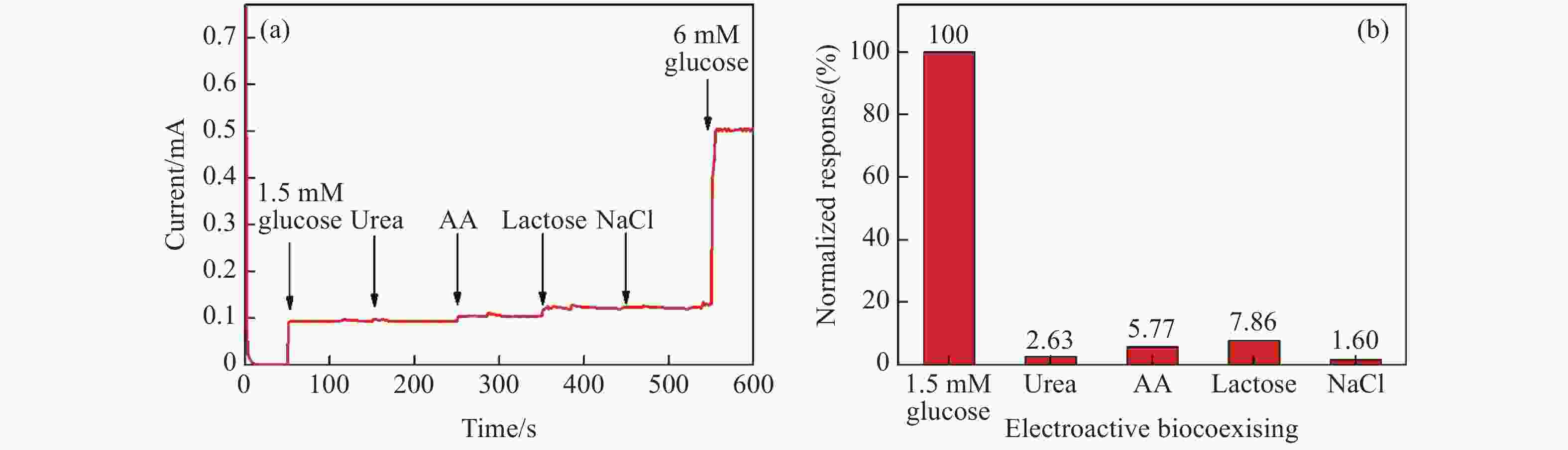
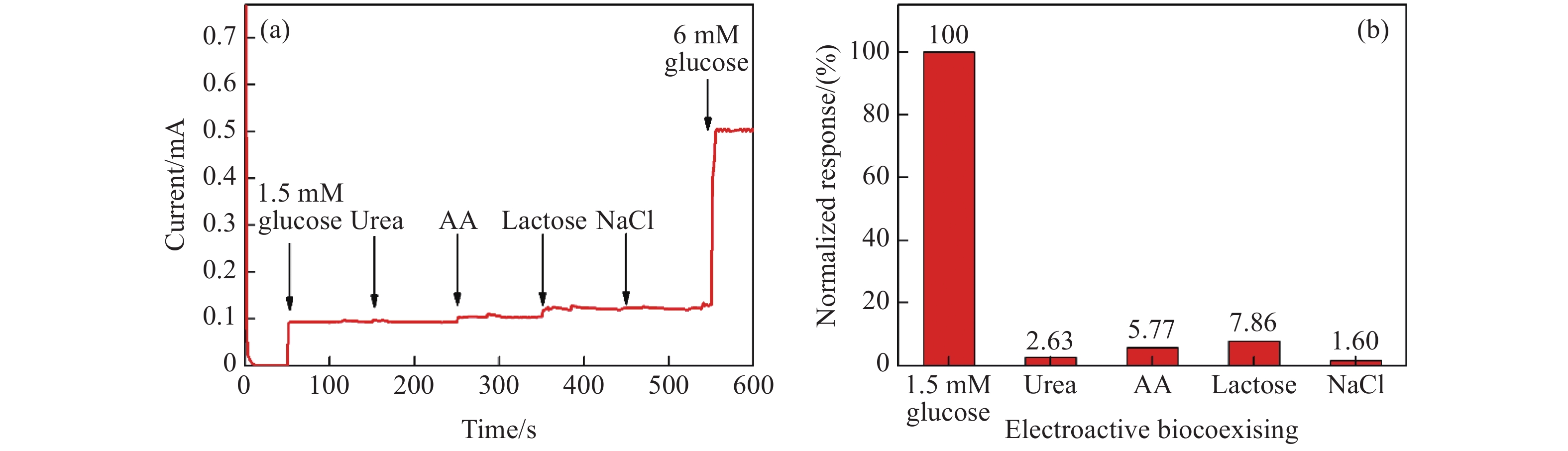
图 11 (a) 0.5 V电压下,在PBS(浓度0.1 mM,pH 7.0)缓冲溶液中连续添加1.5 mM葡萄糖、1 mM Urea、1 mM AA、1 mM乳糖、1 mM NaCl和6 mM葡萄糖时,电极的安培响应;(b) 与目标分析物相比,相应的干扰信号的百分比
Figure 11. (a) Amperometric response of the electrode to the continuous addition of 1.5 mM glucose, 1 mM urea, 1 mM AA, 1 mM lactose, 1 mM NaCl and 6 mM glucose to PBS (0.1 mM, pH 7.0) buffer solution at 0.5 V voltage; (b) the percentage of interfering signals compared with the target analyte
-
[1] ZHONG SH L, ZHUANG J Y, YANG D P, et al. Eggshell membrane-templated synthesis of 3D hierarchical porous Au networks for electrochemical nonenzymatic glucose sensor[J]. Biosensors and Bioelectronics, 2017, 96: 26-32. doi: 10.1016/j.bios.2017.04.038 [2] KAYRAN Y U, JAMBREC D, SCHUHMANN W. Nanostructured DNA microarrays for dual SERS and electrochemical read-out[J]. Electroanalysis, 2019, 31(2): 267-272. doi: 10.1002/elan.201800579 [3] PODESVA P, LIU X CH, PUMERA M, et al. Tailorable nanostructured mercury/gold amalgam electrode arrays with varied surface areas and compositions[J]. Sensors and Actuators B:Chemical, 2020, 302: 127175. doi: 10.1016/j.snb.2019.127175 [4] TANG Y. In(NO3)3 induced tailoring of ZnO Nanorods' optical properties by electrodeposition[J]. Chinese Journal of Luminescence, 2020, 41(5): 571-578. (in Chinese) doi: 10.3788/fgxb20204105.0571 [5] PIYA R, ZHU Y, SOERIYADI A H, et al. Micropatterning of porous silicon Bragg reflectors with poly (ethylene glycol) to fabricate cell microarrays: towards single cell sensing[J]. Biosensors and Bioelectronics, 2019, 127: 229-235. doi: 10.1016/j.bios.2018.12.001 [6] CAI Y H, GAO X, WANG J H, et al. Output characteristics of Broad-area stripe semiconductor lasers with microthermal channel anode structure[J]. Chinese Journal of Luminescence, 2021, 42(4): 518-525. (in Chinese) doi: 10.37188/CJL.20200365 [7] ZHAO W, ZHANG R L, XU SH, et al. Molecularly imprinted polymeric nanoparticles decorated with Au NPs for highly sensitive and selective glucose detection[J]. Biosensors and Bioelectronics, 2018, 100: 497-503. doi: 10.1016/j.bios.2017.09.020 [8] WANG L Y, LIU K W, CHEN X, et al. Fabrication and characteristics of MgZnO ultraviolet detector based on Ag microporous array structure electrode[J]. Chinese Journal of Luminescence, 2021, 42(2): 201-207. (in Chinese) doi: 10.37188/CJL.20200362 [9] MIR M, DONDAPATI S K, DUARTE M V, et al. Electrochemical biosensor microarray functionalized by means of biomolecule friendly photolithography[J]. Biosensors and Bioelectronics, 2010, 25(9): 2115-2121. doi: 10.1016/j.bios.2010.02.012 [10] AN L, WANG G T, HAN Y, et al. Electrochemical biosensor for cancer cell detection based on a surface 3D micro-array[J]. Lab on a Chip, 2018, 18(2): 335-342. doi: 10.1039/C7LC01117B [11] TANG Y, ZHAO Y, ZHANG Z G, et al. Hydrothermal synthesis and properties of ZnO nanorod arrays[J]. Chinese Journal of Materials Research, 2015, 29(7): 529-534. (in Chinese) doi: 10.11901/1005.3093.2014.434 [12] PALA K, SUBHAS C, KUNDUB C, VAMSI K, et al. Biosensing using photolithographically micropatterned electrodes ofPEDOT:PSS on ITO[J]. Sensors and Actuators B:Chemical, 2017, 242: 140-147. doi: 10.1016/j.snb.2016.11.049 [13] XIAO X Z, LÜ C, WANG G, et al. Flexible triboelectric nanogenerator from micro-nano structured polydimethylsiloxane[J]. Chemical Research in Chinese Universities, 2015, 31(3): 434-438. doi: 10.1007/s40242-015-4432-8 [14] RAYMUNDO-PEREIRA P A, SHIMIZU F M, COELHO D, et al. A nanostructured bifunctional platform for sensing of glucose biomarker in artificial saliva: synergy in hybrid Pt/Au surfaces[J]. Biosensors and Bioelectronics, 2016, 86: 369-376. doi: 10.1016/j.bios.2016.06.053 [15] VERMA A K, DAS R, SONI R K. Laser fabrication of periodic arrays of microsquares on silicon for SERS application[J]. Applied Surface Science, 2018, 427: 133-140. doi: 10.1016/j.apsusc.2017.08.143 [16] CHEN R H, LIU H, ZHANG H L, et al. Edge smoothness enhancement in DMD scanning lithography system based on a wobulation technique[J]. Optics Express, 2017, 25(18): 21958-21968. doi: 10.1364/OE.25.021958 [17] XIONG ZH, LIU H, CHEN R H, et al. Illumination uniformity improvement in digital micromirror device based scanning photolithography system[J]. Optics Express, 2018, 26(14): 18597-18607. doi: 10.1364/OE.26.018597 [18] LI Q K, XIAO Y, LIU H, et al. Analysis and correction of the distortion error in a DMD based scanning lithography system[J]. Optics Communications, 2019, 434: 1-6. doi: 10.1016/j.optcom.2018.10.042 [19] ZHANG Y, LUO J, XIONG ZH, et al. User-defined microstructures array fabricated by DMD based multistep lithography with dose modulation[J]. Optics Express, 2019, 27(22): 31956-31966. doi: 10.1364/OE.27.031956 [20] QIU C C, WANG X, LIU X Y, et al. Direct electrochemistry of glucose oxidase immobilized on nanostructured gold thin films and its application to bioelectrochemical glucose sensor[J]. Electrochimica Acta, 2012, 67: 140-146. doi: 10.1016/j.electacta.2012.02.011 -

 下载:
下载:


计量
- 文章访问数: 1045
- HTML全文浏览量: 606
- PDF下载量: 180
- 被引次数: 0
