


Principle and application of metasurface optical field modulation of atomic layer thickness
-
摘要: 超表面由亚波长尺度二维人工微结构构成,可以实现对光场振幅、相位、偏振等多参量进行调控,为光场调控提供了优良平台。二维材料作为一种新型层状结构材料,相对于三维体材料有着十分独特的光学和电学特性,其与超表面结合为纳米尺度平面光学器件的发展提供了新的可能。本文综述了基于原子层厚度的二维材料超表面发展,介绍了多种二维材料超表面光场调控机制、制备以及应用,最后对原子层厚度超表面发展面临的挑战和潜在应用进行展望。Abstract: Metasurfaces, composed of subwavelength-scale artificial nanostructures, can realize the versatile modulation of multiple attributes of light such as amplitude, phase and polarization, providing an excellent platform for nanophotonic devices. As a new type of layered material, 2D materials manifest peculiar optical and electrical properties compared to 3D bulk materials. The combination of 2D materials with metasurfaces offers new possibilities for the development of nanoscale planar optical devices. This paper reviews the development of metasurfaces based on 2D materials with atomic thicknesses, introduces the mechanism of light field modulation of various 2D material metasurfaces. An outlook on the challenges and potential applications for the development of atomic layer thickness metasurfaces are provided finally.
-
Key words:
- metasurface /
- light field modulation /
- two-dimensional materials /
- holography
-
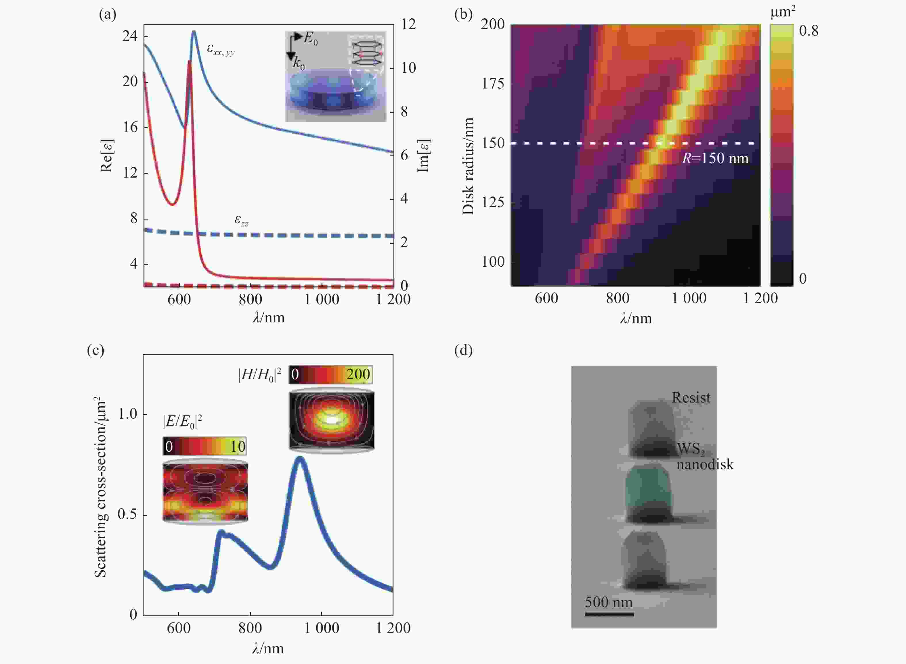
图 1 (a)WS2在面内和面外的介电常数。(b)模拟h=200 nm的多层WS2散射截面的散射与盘半径和波长的对应关系。(c)模拟了h=200 nm和R =150 nm的多层WS2纳米盘在真空中的散射截面。(d)制备的多层WS2全电介质纳米盘的伪彩色侧视扫描电子显微镜(SEM)图像[58]
Figure 1. (a) The in-plane and out-of-plane dielectric constants of WS2. (b) Simulated scattering cross sections of multilayer WS2 at h = 200 nm as a function of disk radius and wavelengths. (c) Simulated scattering cross sections of multilayer WS2 nanodisk at h = 200 nm and R = 150 nm in vacuum. (d) False color side-view Scanning Electron Microscope (SEM) image of the prepared multilayer WS2 all-dielectric nanodisk[58]
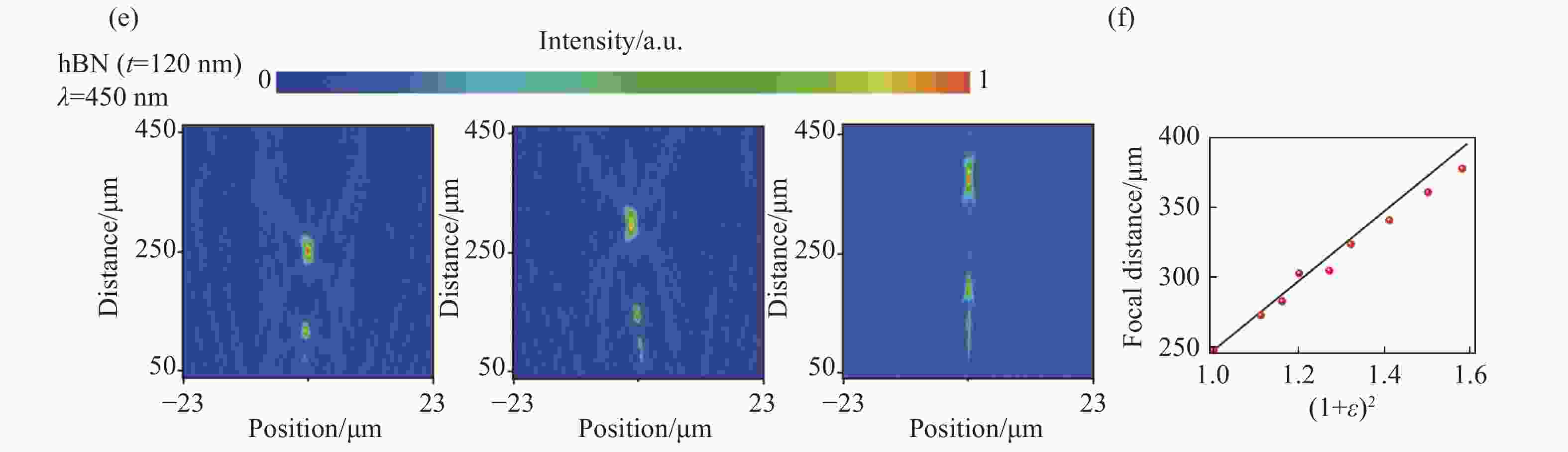
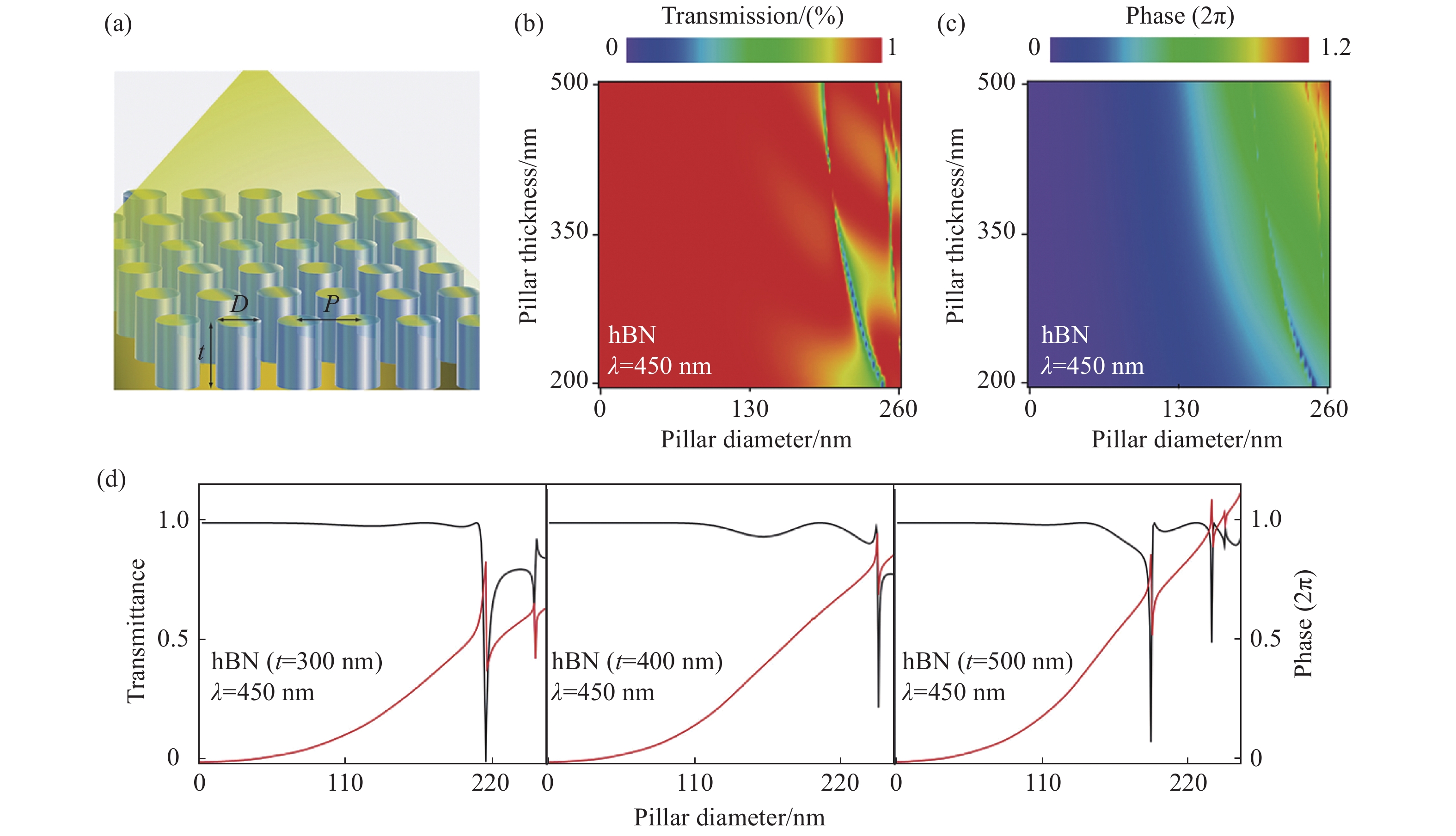
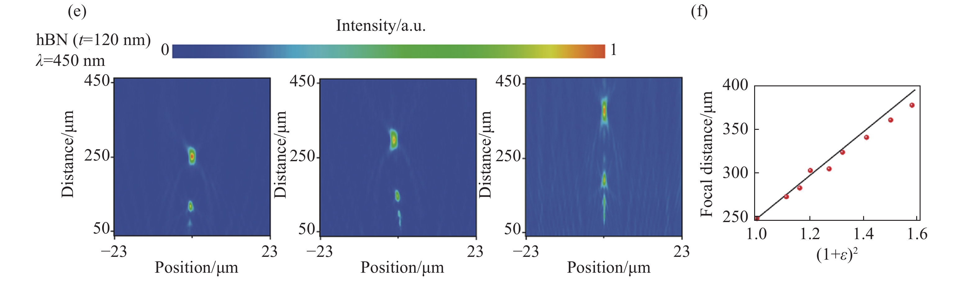
图 2 (a)多层vdW全电介质纳米柱阵列示意图。模拟计算在改变纳米柱尺寸时通过阵列后波前振幅(b)和相位(c)的变化。(d)从左到右:纳米柱的厚度分别固定为300、400和500 nm时,柱直径与透射波前的幅度(黑色)和相位(红色)的对应关系。这些模拟曲线是从图(c)和(d)中对应提取。(e)集成在PDMS柔性基板上的多层h-BN全电介质超透镜的轴向焦场强度分布图。(f)应变诱导的可调谐聚焦效应。数据图为在不同应变值下测得的(圆形符号)和分析预测的(实线)焦距[59]
Figure 2. (a) Schematic diagram of multi-layer vdW all-dielectric nanopillar arrays. The color maps show RCWA providing the change in the (b) amplitude and (c) phase of a wavefront after passing through the array when varying the dimensions of the nanopillars. (d) From left to right: correspondence of nanopillar diameter to the amplitude (black) and phase (red) of the transmitted wavefront when the thickness of the nanopillar is fixed at 300, 400 and 500 nm, respectively. These simulated curves are extracted from Figures (c) and (d), (e), Axial focal field intensity distribution of multi-layer h-BN all-dielectric metalens integrated on PDMS flexible substrate. (f) Strain induced tunable focusing effect. Measured (round symbols) and analytically predicted (solid line) focal lengths under different strain values[59]
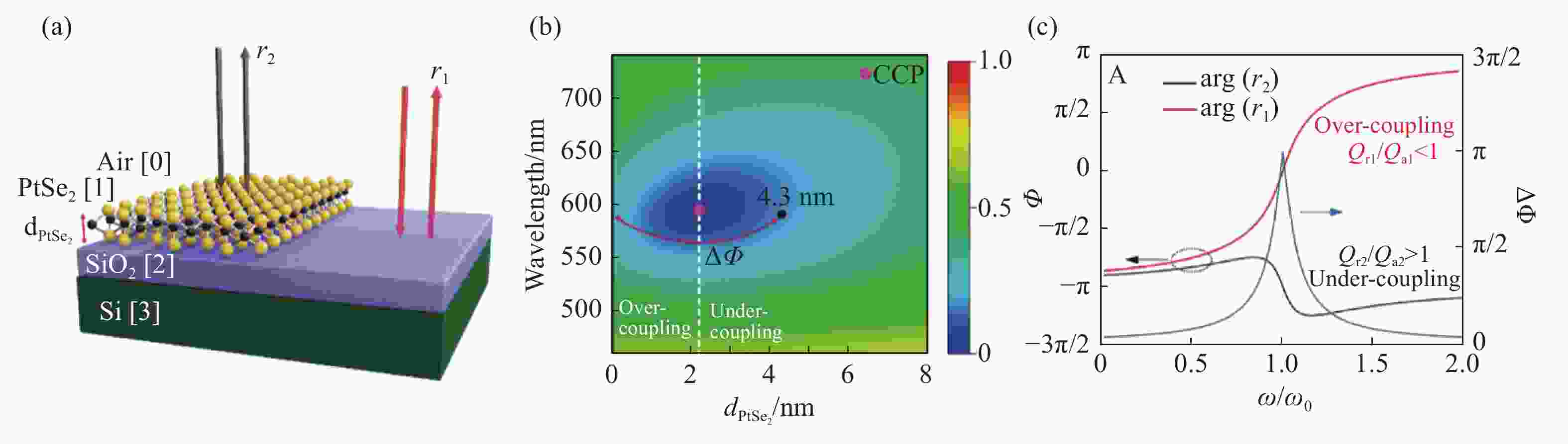
图 3 (a)原子层厚度二元超表面实现Heaviside光学相位调制示意图。(b)PtSe2-SiO2-Si多层膜的反射率与PtSe2厚度和入射波长的关系。(c)过耦合和欠耦合情况下的反射相位谱[65]
Figure 3. (a) Schematic diagram of Heaviside optical phase modulation realized by atomic layer thickness binary metasurface. (b) Reflectance of PtSe2-SiO2-Si multilayers as a function of the PtSe2 thickness and the incident wavelength. (c) Spectra of reflection phase for over- and under-coupling cases[65]

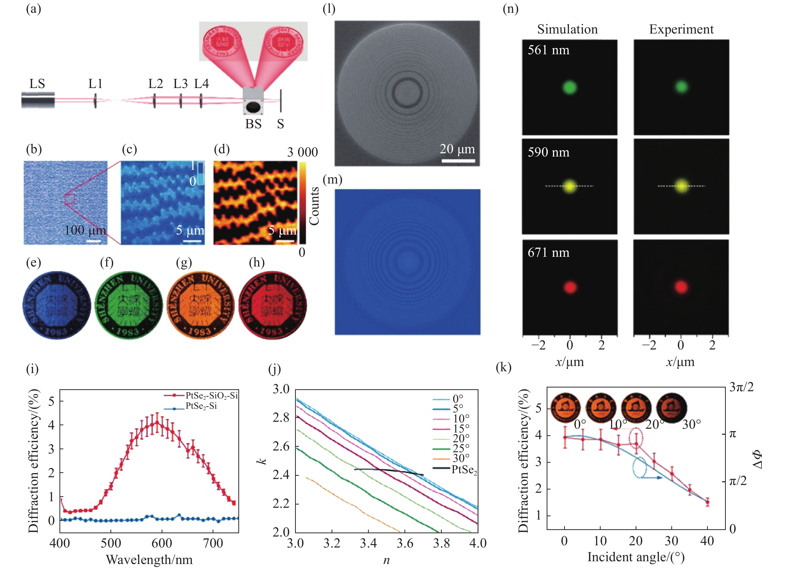
图 4 原子层厚度二元超表面全息成像和超透镜实验效果。(a)构建全息图像的实验装置,(b)激光直写技术制备的二元超表面光学显微镜图像。正方形标记区域的光学图像(c)以及拉曼图像(d)。(e-h)在照明波长分别为473, 561, 590和671 nm的全息重构图像。(i)比较有和没有290 nm厚硅衬底层样品的实测衍射效率。(j)在不同入射角(0°,5°,10°,15°,20°,25°,30°)下,PtSe2薄膜在(n-k)图中的最小反射轨迹和色散情况。(k)测量衍射效率(红色散射)和计算相位差(蓝色曲线)与入射角的关系。菲涅耳波带片平面超透镜的电镜(l)和对应光学(m)图像。(n)3种不同波长聚焦强度分布的模拟结果与实验结果的比较[65]
Figure 4. Demonstration of atomically thin meta-holograms and Fresnel zone plate (FZP) lenses. (a) Experimental configuration for reconstructing holographic images. (b) Optical microscope image of scribed meta-optics pixel arrays by Direct Laser Writing (DLW). The optical image (c) of the square marked area and the Raman image (d). (e-h) Holographic images captured at illumination wavelengths of 473, 561, 590, and 671 nm, respectively. (i) Comparison of measured diffraction efficiencies for the samples with and without the 290-nm thick silica substrate. (j) Minimum reflection trajectories and dispersion of PtSe2 films in (n-k) figures at different incident angles (0°, 5°, 10°, 15°, 20°, 25°, 30°). (k) Measured diffraction efficiencies (red scatters) and calculated phase difference (blue curve) as a function of the incident angle. SEM (l) and corresponding optical images (m) of Fresnel zone plate plane metalens. (n) Cross section of the simulated and experimental intensity distribution of the focal spot at the wavelength of 561, 590, 671 nm[65]
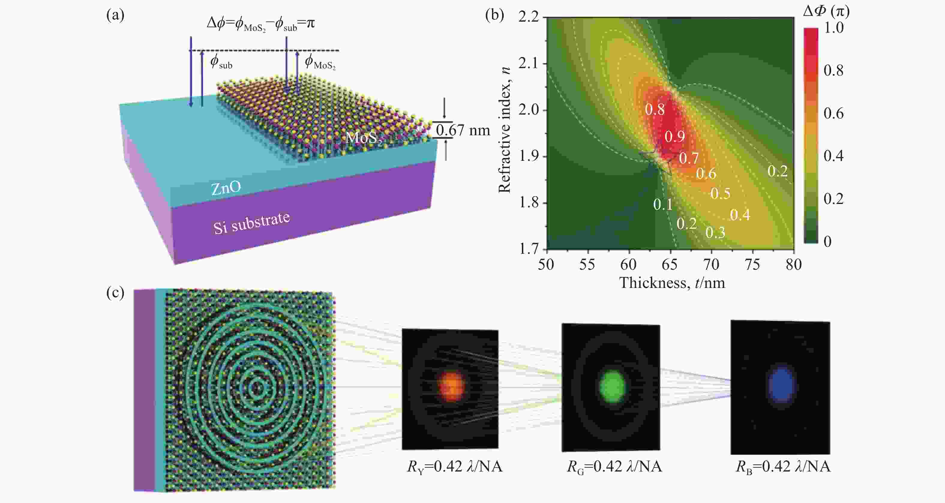
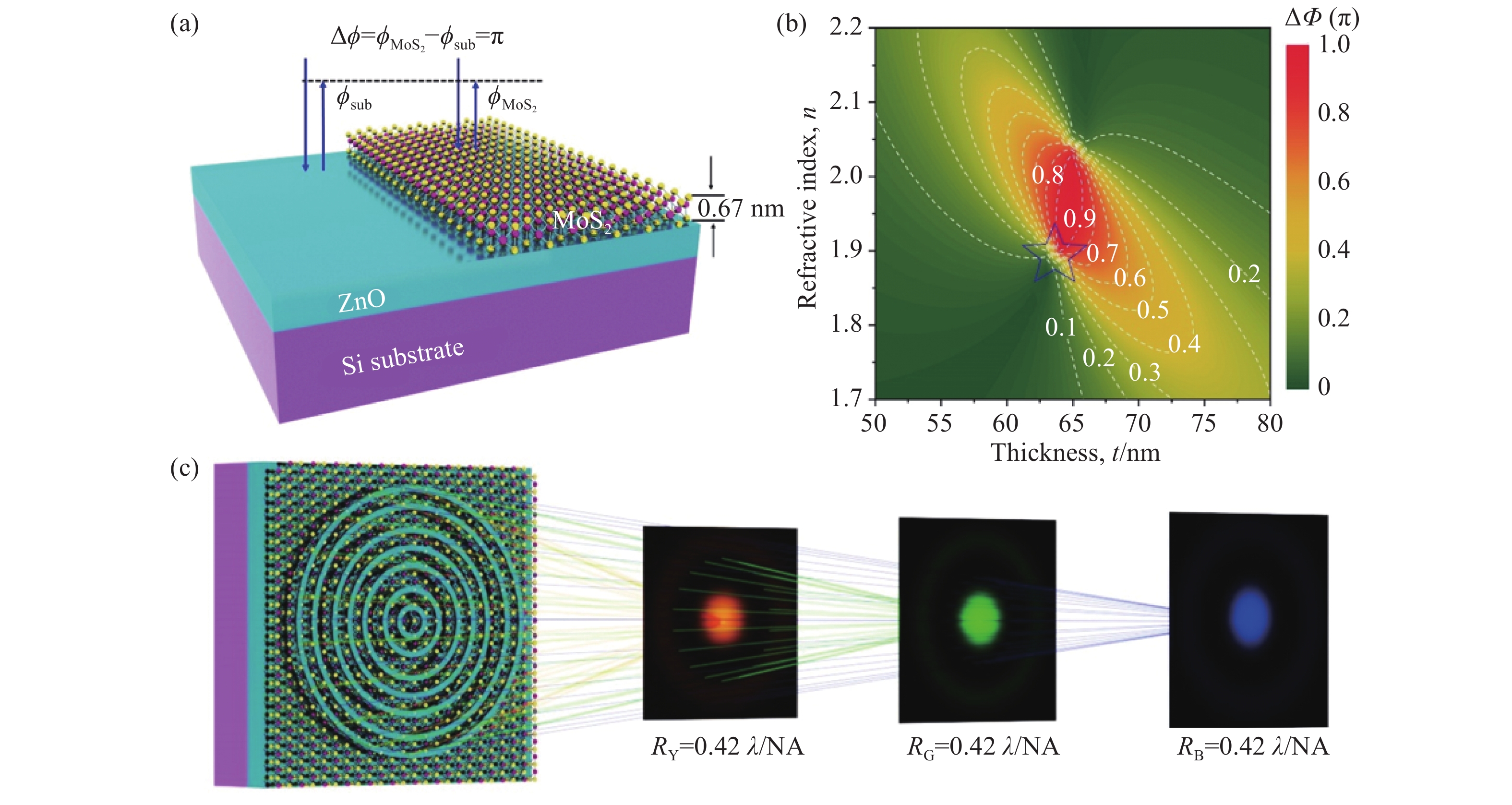
图 5 (a)二硫化钼片和硅衬底之间的反射相移示意图。(b)基于吸收损耗与辐射损耗竞争产生临界耦合条件下的Heaviside相位调制与介质层厚度(t)和折射率(n)的关系。(c)原子层厚度平面超临界透镜及其宽谱超衍射极限聚焦特性[66]
Figure 5. (a) Schematic illustration of the reflected phase shift between MoS2 sheets and silicon substrates. (b) Relation between Heaviside phase modulation and dielectric layer thickness (t) and refractive index (n) under the condition of critical coupling based on the competition between absorption losses and radiation losses. (c) Planar supercritical lens with atomic layer thickness and its wide-spectrum sub-diffraction limited focusing characteristics[66]
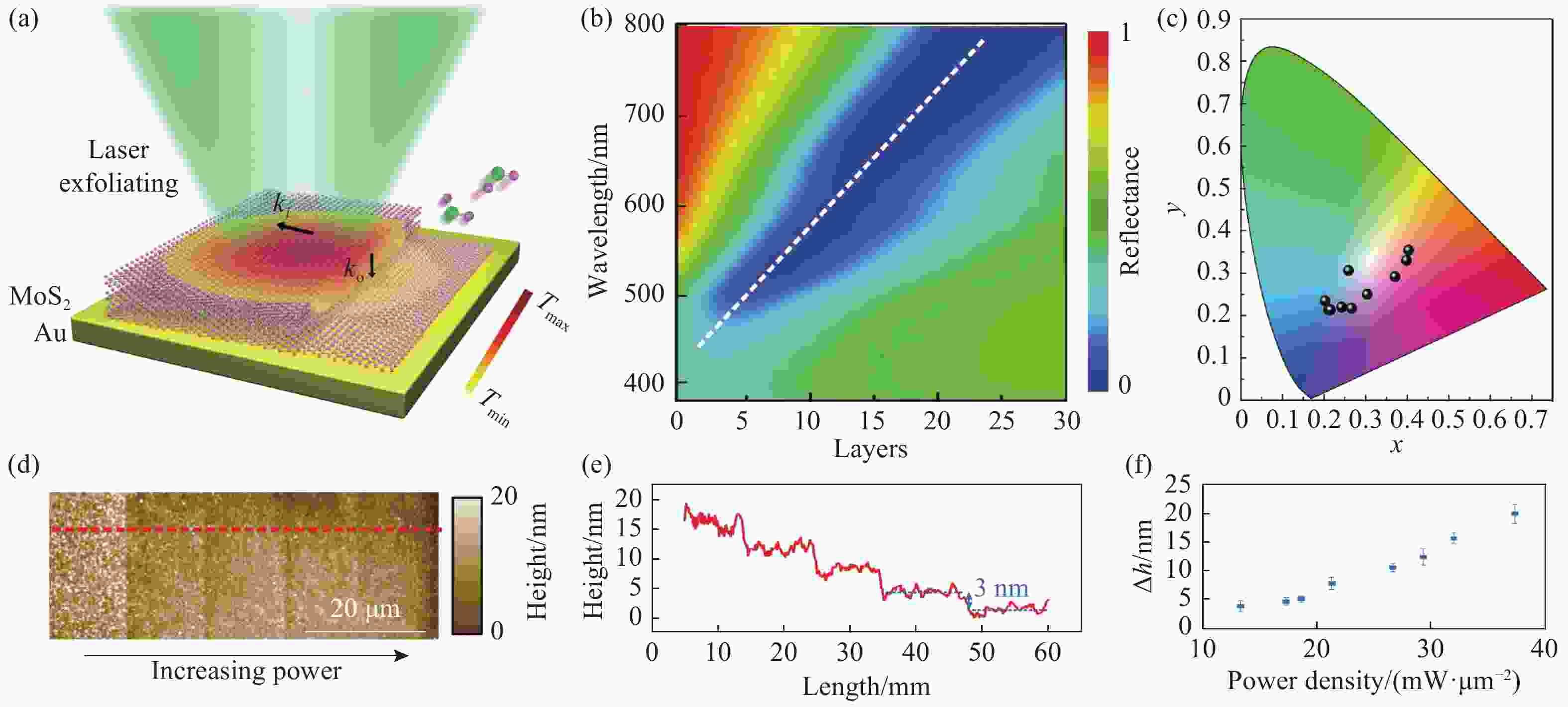
图 6 (a)基于非平凡界面相移的激光削薄少层MoS2薄膜实现谐振波长调控示意图。(b)模拟显示MoS2薄膜涂敷的金属衬底结构反射光谱与MoS2原子层数对应关系。(c)通过不同功率激光削薄实验得到的反射光谱颜色坐标图。(d)不同功率下得到的激光削薄区域的原子力显微镜图(AFM)。(e)红色虚线对应的高度变化。(f)提取不同功率下由拉曼光谱推算的厚度变化[68]
Figure 6. (a) Schematic illustration of tightly focused laser beams for exfoliating multilayer MoS2 with atomic thickness precisions. (b) The calculated reflectance spectra of the MoS2 thin films on the Au substrate with different numbers of layers. (c) Experimentally obtained reflection color palettes and color coordinate diagram through laser exfoliating at variant powers. (d) The AFM image of laser thinned regions obtained at different laser doses. (e) The height change corresponding to the red dotted line. (f) Extracted thickness variation calculated by Raman spectrum under different powers[68]
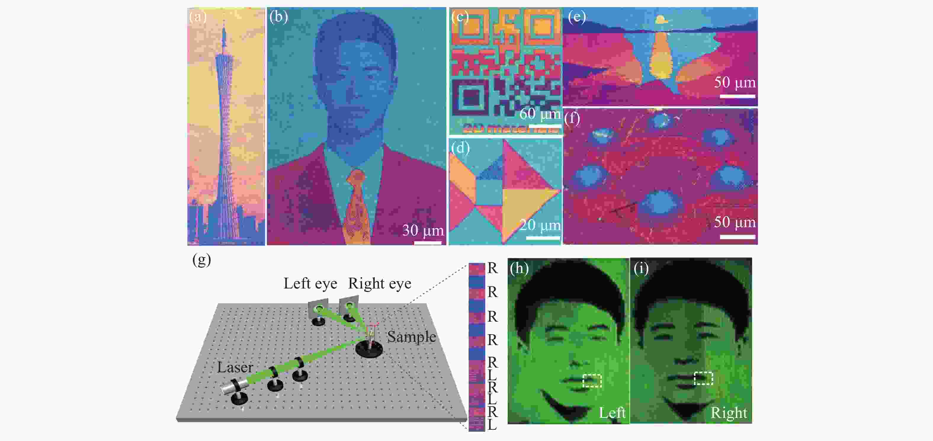
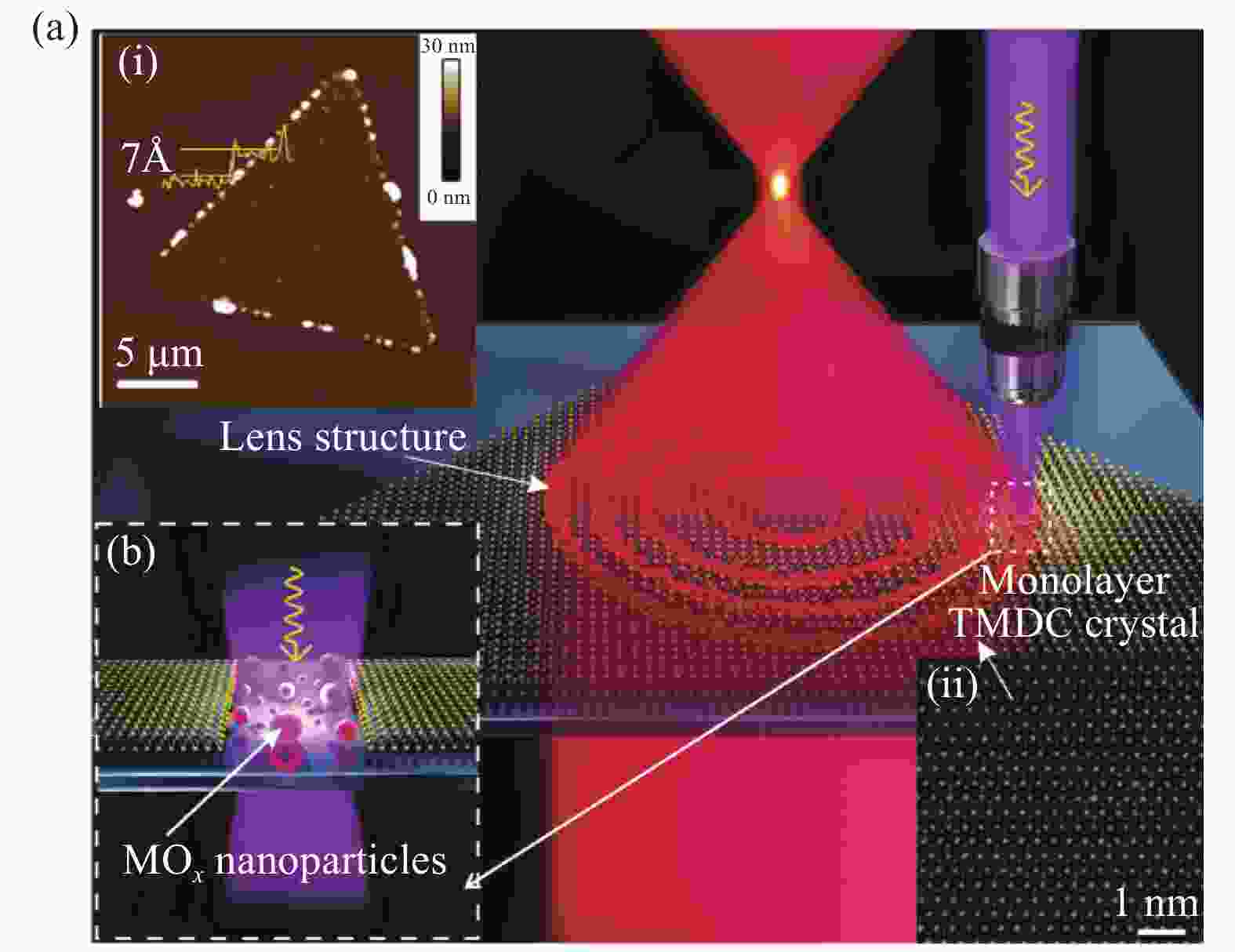
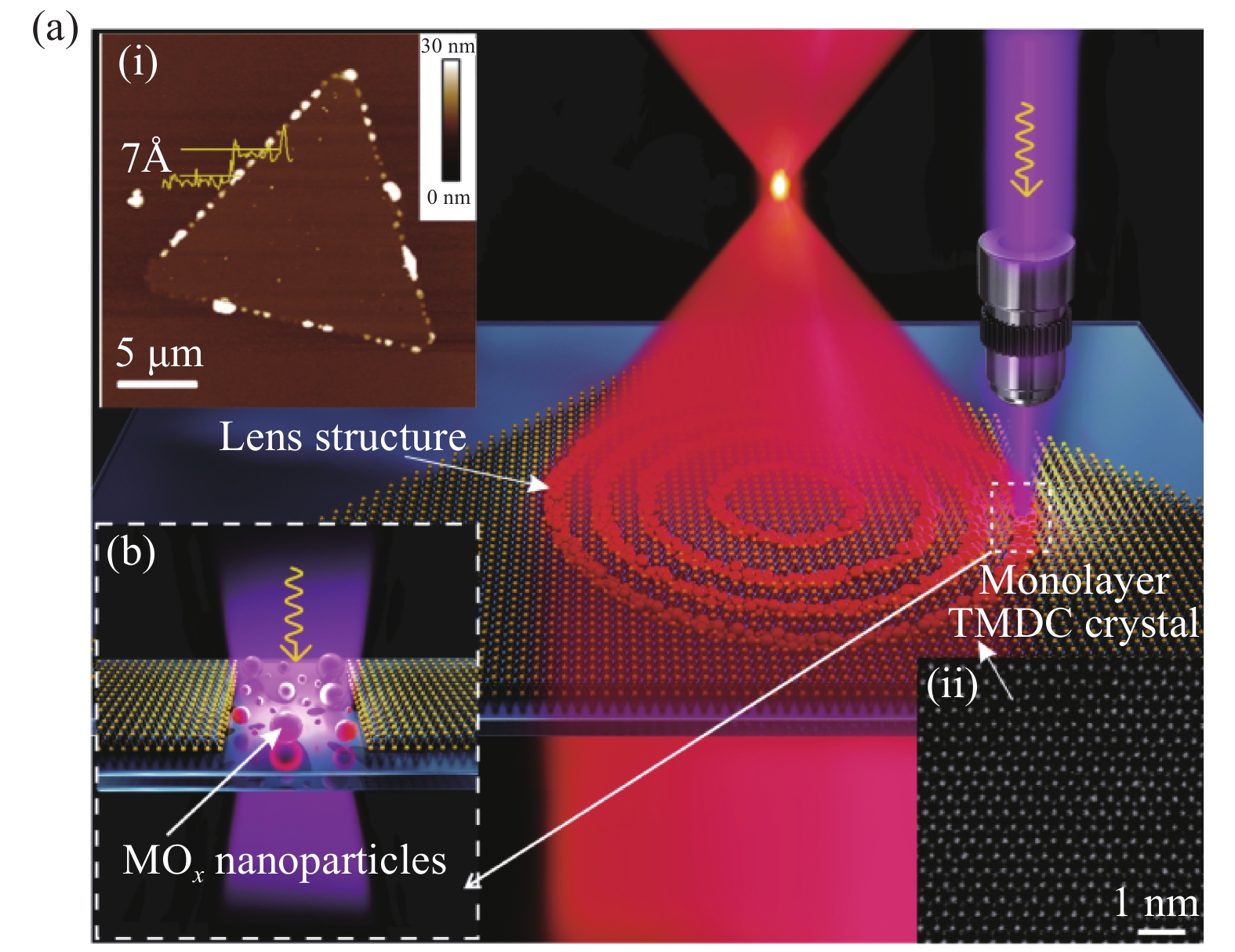
图 8 (a)飞秒激光制造单层TMDC透镜的示意图。插图(i) 单层TMDC(此处为WSe2)单晶的AFM图像,以及(ii) 单层TMDC(此处为WSe2)单晶的STEM图像。(b)飞秒激光诱导生成MOx纳米颗粒的示意图[67]
Figure 8. (a) Schematic of femtosecond laser fabrication of a monolayer TMDC lens. Inset: (i) AFM image of a monolayer TMDC (WSe2 in this case) single crystal, and (ii) STEM image of the monolayer TMDC (WSe2 in this case) single crystal. (b) Schematic of femtosecond laser-induced generation of MOx nanoparticles[67]
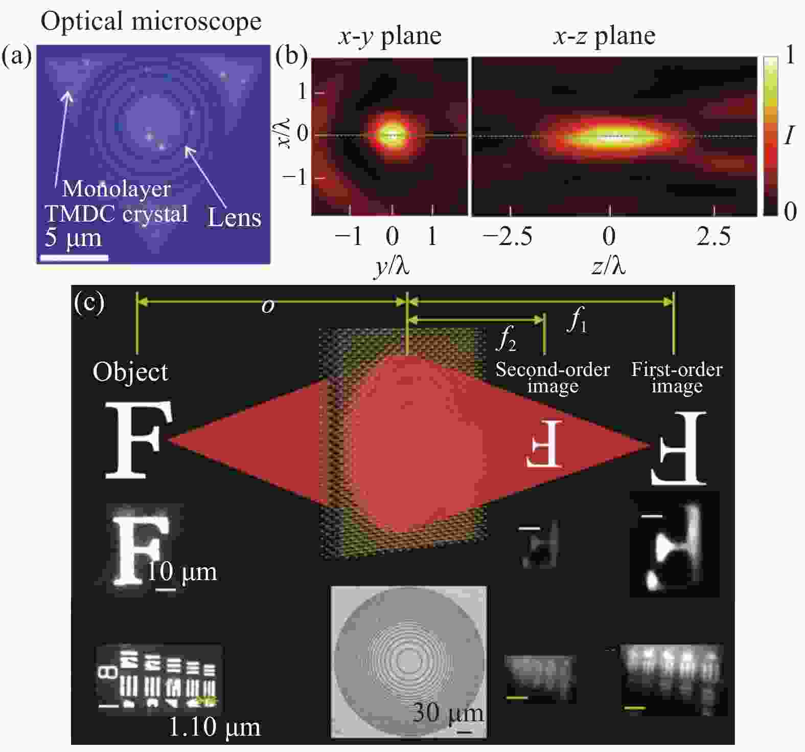
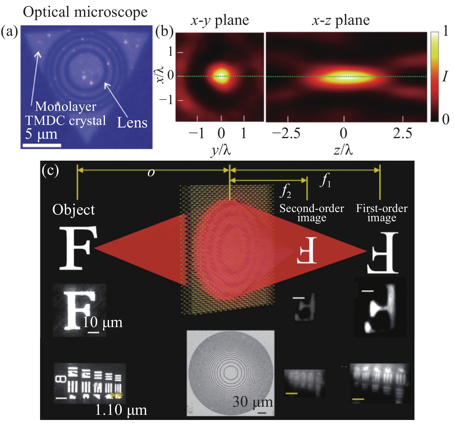
图 9 (a)单原子层WSe2平面透镜的光学显微图像。(b)实验获得的焦点强度在xy和xz平面内的横截面图像。(c)使用单原子层PtS2平面透镜的衍射极限成像的示意图[67]
Figure 9. (a) Optical microscope image of a single atomic layer WSe2 planar lens. (b) Experimentally obtained cross-sectional images of the focal intensity in the xy and xz planes. (c) Schematic illustrating diffraction-limited imaging using a monolayer PtS2 lens[67]
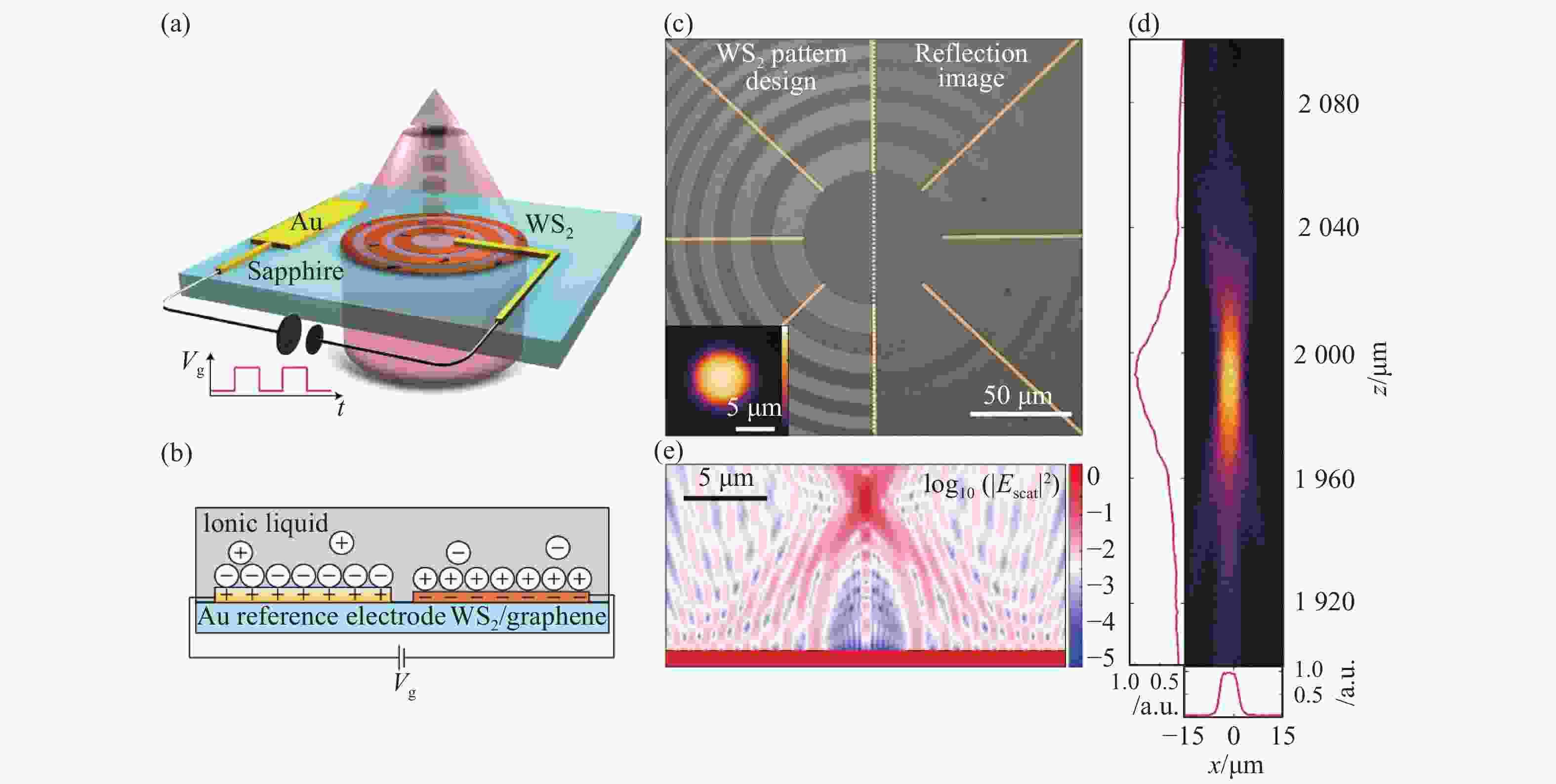
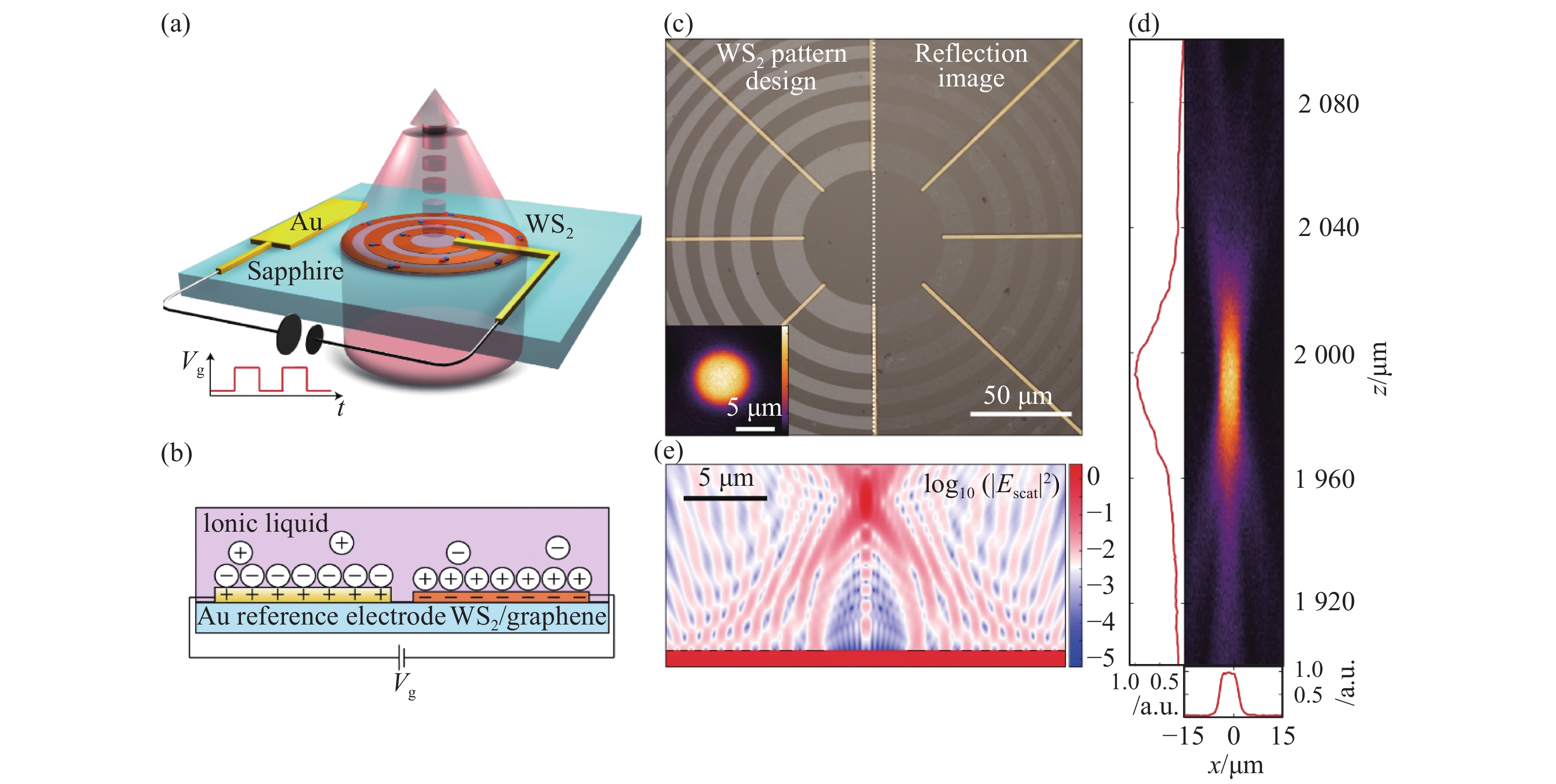
图 10 (a)基于激子共振的可调谐WS2菲涅耳波带片平面透镜示意图。时变的离子-液体栅极电压通过猝灭激子共振而实现聚焦效率的主动调制。(b)离子-液体门控工作原理示意图。(c)加工制作的平面透镜光学显微镜图像(右)和设计的WS2平面透镜图(左)对比。(d)聚焦光束(λ=620 nm)的x-z面内强度分布图。(e)直径为20 μm的菲涅耳波带片平面透镜的散射场强度分布图(λ=620 nm),焦距f =10 μm[69]
Figure 10. (a) Schematic diagram of a Fresnel zone plate tunable WS2 lens based on exciton resonance.Active modulation of focusing efficiency is achieved by quenching exciton resonance through time-varying ion-liquid gate voltage. (b) Schematic diagram of working principle of ion-liquid gating. (c) Comparison between the designed WS2 planar lens (left) and optical microscope image (right) of the fabricated planar lens. (d) Focused beam (λ = 620 nm) intensity distribution in the x z plane. (e) Scattering field intensity distribution of Fresnel zone plate lens with a diameter of 20 μm (λ=620 nm), focal length f = 10 μm[69]
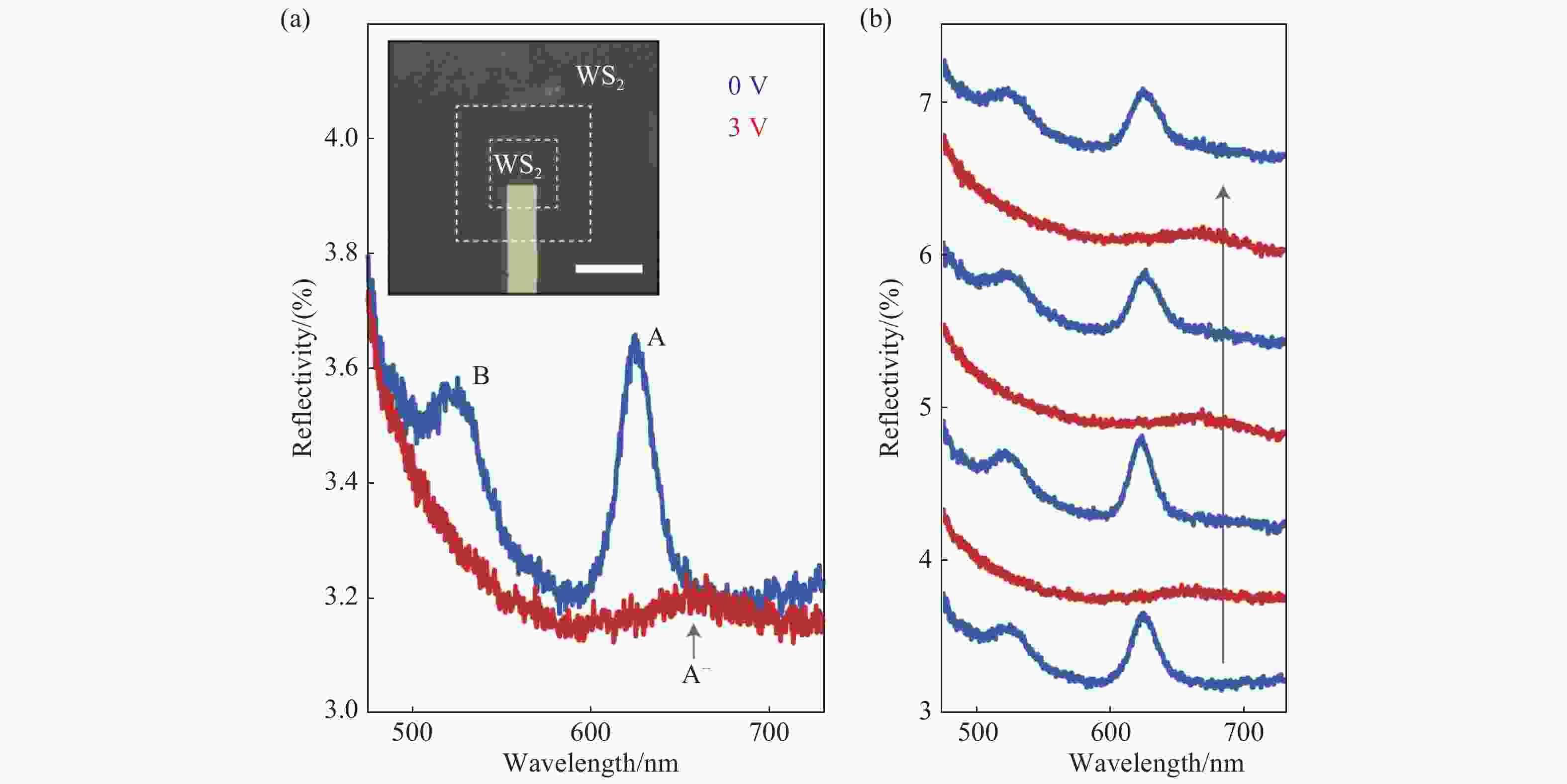
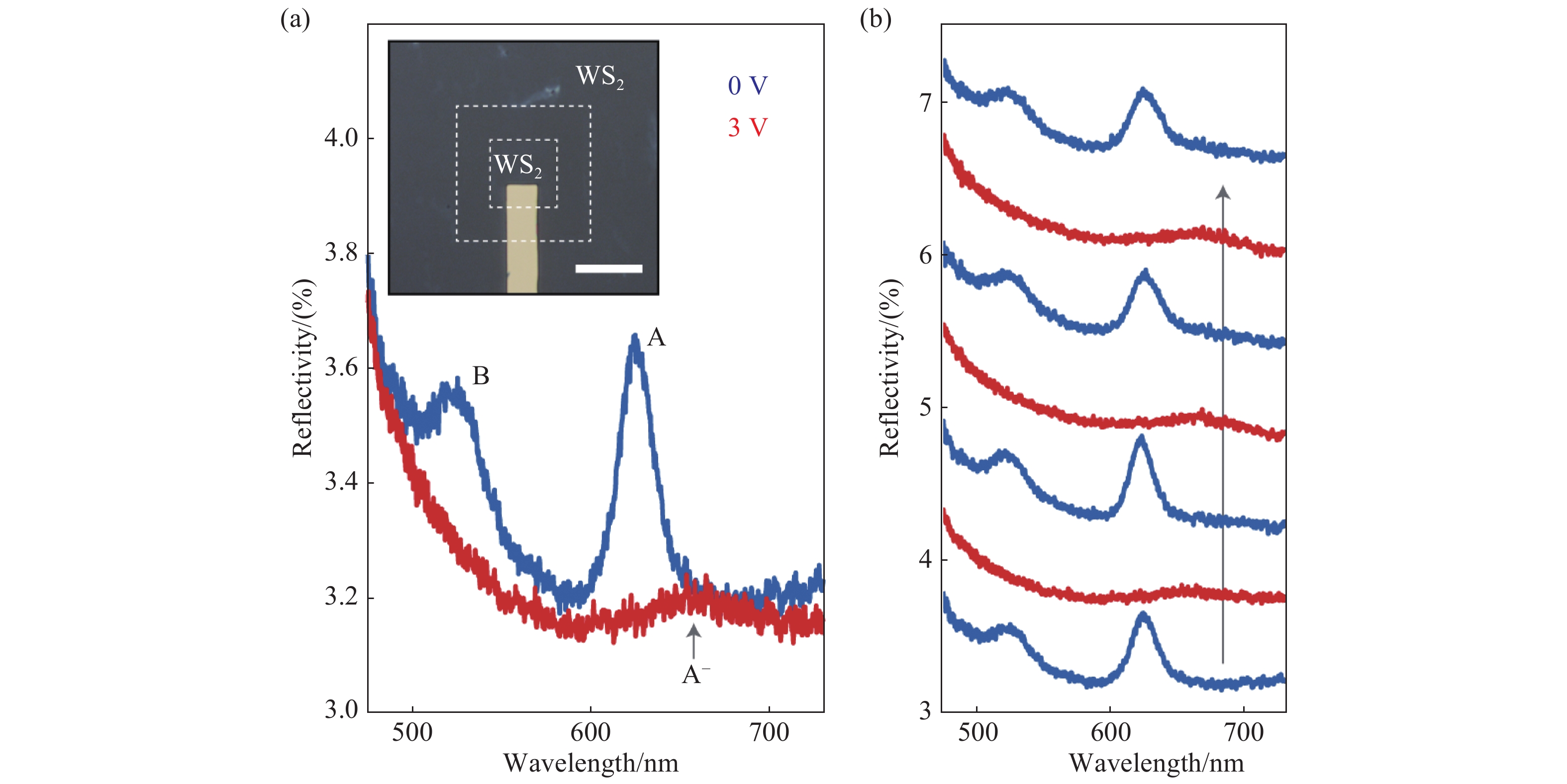
图 11 (a)20 μm×20 μm的单原子层WS2在Vg为0 V和3 V(蓝色和红色)的反射谱。(b)激子共振的可重复调节性。在激子共振态(蓝色)和激子共振淬灭态(红色)之间循环时的反射率光谱[69]
Figure 11. (a) Reflectivity spectra of a 20 μm× 20 µm isolated patch of WS2 for Vg = 0 V (blue) and gated at Vg = 3 V (n-doping, red). (b) Reproducible modulation of exciton resonance. The reflectivity spectrum of cycles between the exciton resonant state (blue) and the exciton resonance-quenched state (red)[69]
-
[1] ENKRICH C, WEGENER M, LINDEN S, et al. Magnetic metamaterials at telecommunication and visible frequencies[J]. Physical Review Letters, 2005, 95(20): 203901. doi: 10.1103/PhysRevLett.95.203901 [2] VALENTINE J, ZHANG SH, ZENTGRAF T, et al. Three-dimensional optical metamaterial with a negative refractive index[J]. Nature, 2008, 455(7211): 376-379. doi: 10.1038/nature07247 [3] WANG L Y, SMITH K W, DOMINGUEZ-MEDINA S, et al. Circular differential scattering of single chiral self-assembled gold nanorod dimers[J]. ACS Photonics, 2015, 2(11): 1602-1610. doi: 10.1021/acsphotonics.5b00395 [4] YU N F, GENEVET P, AIETA F, et al. Flat optics: controlling wavefronts with optical antenna metasurfaces[J]. IEEE Journal of Selected Topics in Quantum Electronics, 2013, 19(3): 4700423. doi: 10.1109/JSTQE.2013.2241399 [5] KUMAR K, DUAN H G, HEGDE R S, et al. Printing colour at the optical diffraction limit[J]. Nature Nanotechnology, 2012, 7(9): 557-561. doi: 10.1038/nnano.2012.128 [6] NI X J, KILDISHEV A V, SHALAEV V M. Metasurface holograms for visible light[J]. Nature Communications, 2013, 4(1): 2807. doi: 10.1038/ncomms3807 [7] CLAUSEN J S, HØJLUND-NIELSEN E, CHRISTIANSEN A B, et al. Plasmonic metasurfaces for coloration of plastic consumer products[J]. Nano Letters, 2014, 14(8): 4499-4504. doi: 10.1021/nl5014986 [8] YU N F, GENEVET P, KATS M A, et al. Light propagation with phase discontinuities: generalized laws of reflection and refraction[J]. Science, 2011, 334(6054): 333-337. doi: 10.1126/science.1210713 [9] YU N F, AIETA F, GENEVET P, et al. A broadband, background-free quarter-wave plate based on plasmonic metasurfaces[J]. Nano Letters, 2012, 12(12): 6328-6333. doi: 10.1021/nl303445u [10] CHEN W T, YANG K Y, WANG C M, et al. High-efficiency broadband meta-hologram with polarization-controlled dual images[J]. Nano Letters, 2014, 14(1): 225-230. doi: 10.1021/nl403811d [11] GAO L H, CHENG Q, YANG J, et al. Broadband diffusion of terahertz waves by multi-bit coding metasurfaces[J]. Light:Science &Applications, 2015, 4(9): e324. [12] MUELLER J P B, RUBIN N A, DEVLIN R C, et al. Metasurface polarization optics: independent phase control of arbitrary orthogonal states of polarization[J]. Physical Review Letters, 2017, 118(11): 113901. doi: 10.1103/PhysRevLett.118.113901 [13] WEN D D, YUE F Y, LI G X, et al. Helicity multiplexed broadband metasurface holograms[J]. Nature Communications, 2015, 6: 8241. doi: 10.1038/ncomms9241 [14] DENG Z L, JIN M K, YE X, et al. Full‐color complex‐amplitude vectorial holograms based on multi‐freedom metasurfaces[J]. Advanced Functional Materials, 2020, 30(21): 1910610. doi: 10.1002/adfm.201910610 [15] LI X, CHEN L W, LI Y, et al. Multicolor 3D meta-holography by broadband plasmonic modulation[J]. Science Advances, 2016, 2(11): e1601102. doi: 10.1126/sciadv.1601102 [16] SUN SH L, YANG K Y, WANG C M, et al. High-efficiency broadband anomalous reflection by gradient meta-surfaces[J]. Nano Letters, 2012, 12(12): 6223-6229. doi: 10.1021/nl3032668 [17] ZHENG G X, MÜHLENBERND H, KENNEY M, et al. Metasurface holograms reaching 80% efficiency[J]. Nature Nanotechnology, 2015, 10(4): 308-312. doi: 10.1038/nnano.2015.2 [18] DENG J, YANG Y, TAO J, et al. Spatial frequency multiplexed meta-holography and meta-nanoprinting[J]. ACS Nano, 2019, 13(8): 9237-9246. doi: 10.1021/acsnano.9b03738 [19] AIETA F, GENEVET P, KATS M A, et al. Aberration-free ultrathin flat lenses and axicons at telecom wavelengths based on plasmonic metasurfaces[J]. Nano Letters, 2012, 12(9): 4932-4936. doi: 10.1021/nl302516v [20] CHEN W T, ZHU A Y, SANJEEV V, et al. A broadband achromatic metalens for focusing and imaging in the visible[J]. Nature Nanotechnology, 2018, 13(3): 220-226. doi: 10.1038/s41565-017-0034-6 [21] WANG SH M, WU P C, SU V C, et al. Broadband achromatic optical metasurface devices[J]. Nature Communications, 2017, 8(1): 187. doi: 10.1038/s41467-017-00166-7 [22] WANG SH M, WU P C, SU V C, et al. A broadband achromatic metalens in the visible[J]. Nature Nanotechnology, 2018, 13(3): 227-232. doi: 10.1038/s41565-017-0052-4 [23] TORRIJOS-MORÁN L, GRIOL A, GARCÍA-RUPÉREZ J. Slow light bimodal interferometry in one-dimensional photonic crystal waveguides[J]. Light:Science &Applications, 2021, 10(1): 16. [24] SUN W J, HE Q, SUN SH L, et al. High-efficiency surface plasmon meta-couplers: concept and microwave-regime realizations[J]. Light:Science &Applications, 2016, 5(1): e16003. [25] XU T, ZHAO Y H, GAN D CH, et al. Directional excitation of surface plasmons with subwavelength slits[J]. Applied Physics Letters, 2008, 92(10): 101501. doi: 10.1063/1.2894183 [26] HUANG L L, CHEN X ZH, MÜHLENBERND H, et al. Dispersionless phase discontinuities for controlling light propagation[J]. Nano Letters, 2012, 12(11): 5750-5755. doi: 10.1021/nl303031j [27] PU M B, LI X, MA X L, et al. Catenary optics for achromatic generation of perfect optical angular momentum[J]. Science Advances, 2015, 1(9): e1500396. doi: 10.1126/sciadv.1500396 [28] BIENER G, NIV A, KLEINER V, et al. Formation of helical beams by use of Pancharatnam–Berry phase optical elements[J]. Optics Letters, 2002, 27(21): 1875-1877. doi: 10.1364/OL.27.001875 [29] SUN SH L, HE Q, XIAO SH Y, et al. Gradient-index meta-surfaces as a bridge linking propagating waves and surface waves[J]. Nature Materials, 2012, 11(5): 426-431. doi: 10.1038/nmat3292 [30] DECKER M, STAUDE I, FALKNER M, et al. High-efficiency dielectric huygens’ surfaces[J]. Advanced Optical Materials, 2015, 3(6): 813-820. doi: 10.1002/adom.201400584 [31] ARBABI A, HORIE Y, BAGHERI M, et al. Dielectric metasurfaces for complete control of phase and polarization with subwavelength spatial resolution and high transmission[J]. Nature Nanotechnology, 2015, 10(11): 937-943. doi: 10.1038/nnano.2015.186 [32] LIN J, GENEVET P, KATS M A, et al. Nanostructured holograms for broadband manipulation of vector beams[J]. Nano Letters, 2013, 13(9): 4269-4274. doi: 10.1021/nl402039y [33] DENG Z L, DENG J H, ZHUANG X, et al. Diatomic metasurface for vectorial holography[J]. Nano Letters, 2018, 18(5): 2885-2892. doi: 10.1021/acs.nanolett.8b00047 [34] KHORASANINEJAD M, AMBROSIO A, KANHAIYA P, et al. Broadband and chiral binary dielectric meta-holograms[J]. Science Advances, 2016, 2(5): e1501258. doi: 10.1126/sciadv.1501258 [35] BHASU V C J, SATHYANARAYANA D N, PATEL C C, et al. Proceedings of the Indian academy of sciences—section A—volume 88–1979[J]. Proceedings of the Indian Academy of Sciences-Chemical Sciences, 1979, 88(4): 333. [36] BERRY M V. Quantal phase factors accompanying adiabatic changes[J]. Proceedings of the Royal Society A:Mathematical,Physical and Engineering Sciences, 1984, 392(1802): 45-57. [37] LIN D M, FAN P Y, HASMAN E, et al. Dielectric gradient metasurface optical elements[J]. Science, 2014, 345(6194): 298-302. doi: 10.1126/science.1253213 [38] HUANG L J, CHEN X ZH, MÜHLENBERND H, et al. Three-dimensional optical holography using a plasmonic metasurface[J]. Nature Communications, 2013, 4(1): 2808. doi: 10.1038/ncomms3808 [39] TAN S J, ZHANG L, ZHU D, et al. Plasmonic color palettes for photorealistic printing with aluminum nanostructures[J]. Nano Letters, 2014, 14(7): 4023-4029. doi: 10.1021/nl501460x [40] LUO X G, PU M B, MA X L, et al. Taming the electromagnetic boundaries via metasurfaces: from theory and fabrication to functional devices[J]. International Journal of Antennas and Propagation, 2015, 2015: 204127. [41] LUO X G. Principles of electromagnetic waves in metasurfaces[J]. Science China Physics,Mechanics &Astronomy, 2015, 58(9): 594201. [42] WEST P R, STEWART J L, KILDISHEV A V, et al. All-dielectric subwavelength metasurface focusing lens[J]. Optics Express, 2014, 22(21): 26212-26221. doi: 10.1364/OE.22.026212 [43] LALANNE P, ASTILEAN S, CHAVEL P, et al. Blazed binary subwavelength gratings with efficiencies larger than those of conventional échelette gratings[J]. Optics Letters, 1998, 23(14): 1081-1083. doi: 10.1364/OL.23.001081 [44] KHORASANINEJAD M, CHEN W T, DEVLIN R C, et al. Metalenses at visible wavelengths: diffraction-limited focusing and subwavelength resolution imaging[J]. Science, 2016, 352(6290): 1190-1194. doi: 10.1126/science.aaf6644 [45] BROWN B R, LOHMANN A W. Complex spatial filtering with binary masks[J]. Applied Optics, 1966, 5(6): 967-969. doi: 10.1364/AO.5.000967 [46] GEIM A K, NOVOSELOV K S. The rise of graphene[J]. Nature Materials, 2007, 6(3): 183-191. doi: 10.1038/nmat1849 [47] WANG Q H, KALANTAR-ZADEH K, KIS A, et al. Electronics and optoelectronics of two-dimensional transition metal dichalcogenides[J]. Nature Nanotechnology, 2012, 7(11): 699-712. doi: 10.1038/nnano.2012.193 [48] MAK K F, LEE C, HONE J, et al. Atomically thin MoS2: a new direct-gap semiconductor[J]. Physical Review Letters, 2010, 105(13): 136805. doi: 10.1103/PhysRevLett.105.136805 [49] PAKDEL A, BANDO Y, GOLBERG D. Nano boron nitride flatland[J]. Chemical Society Reviews, 2014, 43(3): 934-959. doi: 10.1039/C3CS60260E [50] DEAN C R, YOUNG A F, MERIC I, et al. Boron nitride substrates for high-quality graphene electronics[J]. Nature Nanotechnology, 2010, 5(10): 722-726. doi: 10.1038/nnano.2010.172 [51] HULTGREN R, GINGRICH N S, WARREN B E. The atomic distribution in red and black phosphorus and the crystal structure of black phosphorus[J]. The Journal of Chemical Physics, 1935, 3(6): 351-355. doi: 10.1063/1.1749671 [52] SPLENDIANI A, SUN L, ZHANG Y B, et al. Emerging photoluminescence in monolayer MoS2[J]. Nano Letters, 2010, 10(4): 1271-1275. doi: 10.1021/nl903868w [53] MAK K F, HE K L, SHAN J, et al. Control of valley polarization in monolayer MoS2 by optical helicity[J]. Nature Nanotechnology, 2012, 7(8): 494-498. doi: 10.1038/nnano.2012.96 [54] YE Z L, CAO T, O’BRIEN K, et al. Probing excitonic dark states in single-layer tungsten disulphide[J]. Nature, 2014, 513(7517): 214-218. doi: 10.1038/nature13734 [55] WU Y Q, JENKINS K A, VALDES-GARCIA A, et al. State-of-the-art graphene high-frequency electronics[J]. Nano Letters, 2012, 12(6): 3062-3067. doi: 10.1021/nl300904k [56] BALANDIN A A, GHOSH S, BAO W ZH, et al. Superior thermal conductivity of single-layer graphene[J]. Nano Letters, 2008, 8(3): 902-907. doi: 10.1021/nl0731872 [57] WILSON J A, YOFFE A D. The transition metal dichalcogenides discussion and interpretation of the observed optical, electrical and structural properties[J]. Advances in Physics, 1969, 18(73): 193-335. doi: 10.1080/00018736900101307 [58] VERRE R, BARANOV D G, MUNKHBAT B, et al. Transition metal dichalcogenide nanodisks as high-index dielectric Mie nanoresonators[J]. Nature Nanotechnology, 2019, 14(7): 679-683. doi: 10.1038/s41565-019-0442-x [59] LIU CH H, ZHENG J J, COLBURN S, et al. Ultrathin van der Waals metalenses[J]. Nano Letters, 2018, 18(11): 6961-6966. doi: 10.1021/acs.nanolett.8b02875 [60] MORENO I, CAMPOS J, GORECKI C, et al. Effects of amplitude and phase mismatching errors in the generation of a kinoform for pattern recognition[J]. Japanese Journal of Applied Physics, 1995, 34(12R): 6423. [61] LI X P, REN H R, CHEN X, et al. A thermally photoreduced graphene oxides for three-dimensional holographic images[J]. Nature Communications, 2015, 6(1): 6984. doi: 10.1038/ncomms7984 [62] LI P N, DOLADO I, ALFARO-MOZAZ F J, et al. Infrared hyperbolic metasurface based on nanostructured van der Waals materials[J]. Science, 2018, 359(6378): 892-896. doi: 10.1126/science.aaq1704 [63] BAO Q L, ZHANG H, WANG B, et al. Broadband graphene polarizer[J]. Nature Photonics, 2011, 5(7): 411-415. doi: 10.1038/nphoton.2011.102 [64] KIM S, JANG M S, BRAR V W, et al. Electronically tunable perfect absorption in graphene[J]. Nano Letters, 2018, 18(2): 971-979. doi: 10.1021/acs.nanolett.7b04393 [65] WANG Y W, DENG Z L, HU D J, et al. Atomically thin noble metal dichalcogenides for phase-regulated meta-optics[J]. Nano Letters, 2020, 20(11): 7811-7818. doi: 10.1021/acs.nanolett.0c01805 [66] QIN F, LIU B Q, ZHU L W, et al. π-phase modulated monolayer supercritical lens[J]. Nature Communications, 2021, 12(1): 32. doi: 10.1038/s41467-020-20278-x [67] LIN H, XU Z Q, CAO G Y, et al. Diffraction-limited imaging with monolayer 2D material-based ultrathin flat lenses[J]. Light:Science &Applications, 2020, 9(1): 137. [68] HU D J, LI H, ZHU Y P, et al. Ultra-sensitive nanometric flat laser prints for binocular stereoscopic image[J]. Nature Communications, 2021, 12(1): 1154. doi: 10.1038/s41467-021-21499-4 [69] VAN DE GROEP J, SONG J H, CELANO U, et al. Exciton resonance tuning of an atomically thin lens[J]. Nature Photonics, 2020, 14(7): 426-430. doi: 10.1038/s41566-020-0624-y [70] QU CH, MA SH J, HAO J M, et al. Tailor the functionalities of metasurfaces based on a complete phase diagram[J]. Physical Review Letters, 2015, 115(23): 235503. doi: 10.1103/PhysRevLett.115.235503 [71] LOPEZ-SANCHEZ O, LEMBKE D, KAYCI M, et al. Ultrasensitive photodetectors based on monolayer MoS2[J]. Nature Nanotechnology, 2013, 8(7): 497-501. doi: 10.1038/nnano.2013.100 [72] ANDRZEJEWSKI D, HOPMANN E, JOHN M, et al. WS2 monolayer-based light-emitting devices in a vertical p–n architecture[J]. Nanoscale, 2019, 11(17): 8372-8379. doi: 10.1039/C9NR01573F [73] DOBUSCH L, SCHULER S, PEREBEINOS V, et al. Thermal light emission from monolayer MoS2[J]. Advanced Materials, 2017, 29(31): 1701304. doi: 10.1002/adma.201701304 [74] YANG J, WANG ZH, WANG F, et al. Atomically thin optical lenses and gratings[J]. Light:Science &Applications, 2016, 5(3): e16046. [75] KATS M A, BLANCHARD R, GENEVET P, et al. Nanometre optical coatings based on strong interference effects in highly absorbing media[J]. Nature Materials, 2013, 12(1): 20-24. doi: 10.1038/nmat3443 [76] WANG Z, YUAN G H, YANG M, et al. Exciton-enabled meta-optics in two-dimensional transition metal dichalcogenides[J]. Nano Letters, 2020, 20(11): 7964-7972. doi: 10.1021/acs.nanolett.0c02712 -

 下载:
下载:


计量
- 文章访问数: 2793
- HTML全文浏览量: 1389
- PDF下载量: 375
- 被引次数: 0
