


-
摘要: 随着大规模集成电路芯片制造的技术节点不断缩小,光刻机的聚焦控制变得尤为困难。为了保证硅片曝光的质量,需要快速、准确地将硅片在几十纳米的聚焦深度范围(DOF)内进行快速调整。因此,需要仔细分析光刻过程中导致焦点偏移或工艺窗口变化的各种因素,制定合理的聚焦控制预算,将各种误差因素控制在一定范围内。本文聚焦极紫外(EUV)光刻,综述包含EUV在内的先进光刻机中光路部分对聚焦控制有影响的各种因素,总结它们产生的原理及仿真、实验结果,为开展先进光刻聚焦控制预算研究提供参考。Abstract: As the technology node of large-scale integrated circuits continues to shrink, the focus control of the lithographic tools becomes particularly difficult. In order to ensure the exposure quality of wafers, it is necessary to quickly and accurately adjust the wafer in the Depth of Focus (DOF) to a degree as small as few dozen of nanometers. For this reason, people need to carefully analyze the various factors that cause defocusing or process window changes in the lithographic process, make a reasonable focus control budget, and control the various error factors within a certain range. This paper focuses on Extreme Ultraviolet (EUV) lithography, reviews the factors that affect focus control in the optical path of an advanced EUV lithographic tool and summarizes their principles, simulation and experimental results. It can provide a reference when conducting advanced lithography focus control budget research.
-
Key words:
- focus control /
- lithography /
- budget /
- best focus /
- depth of focus /
- process window
-
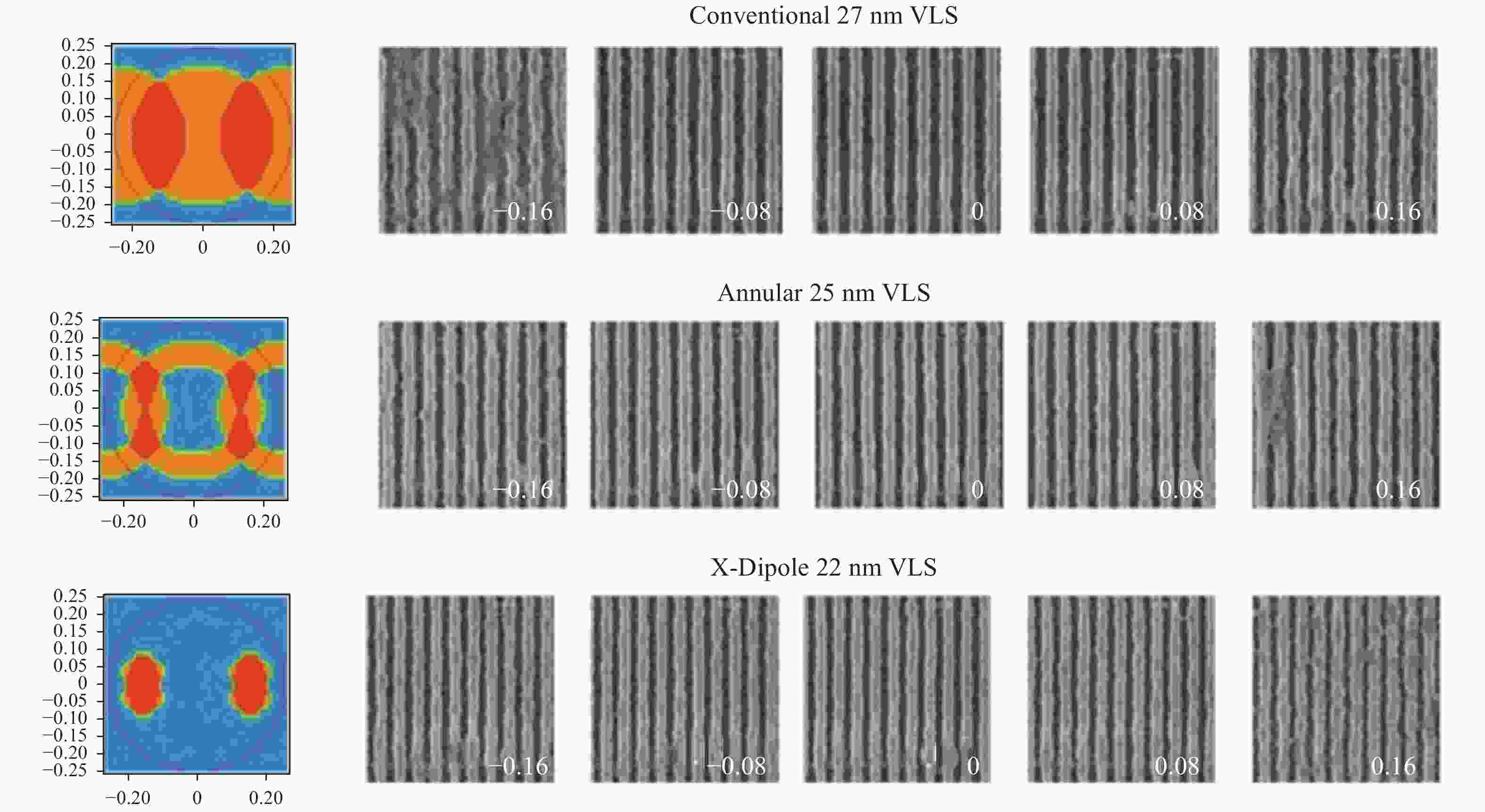
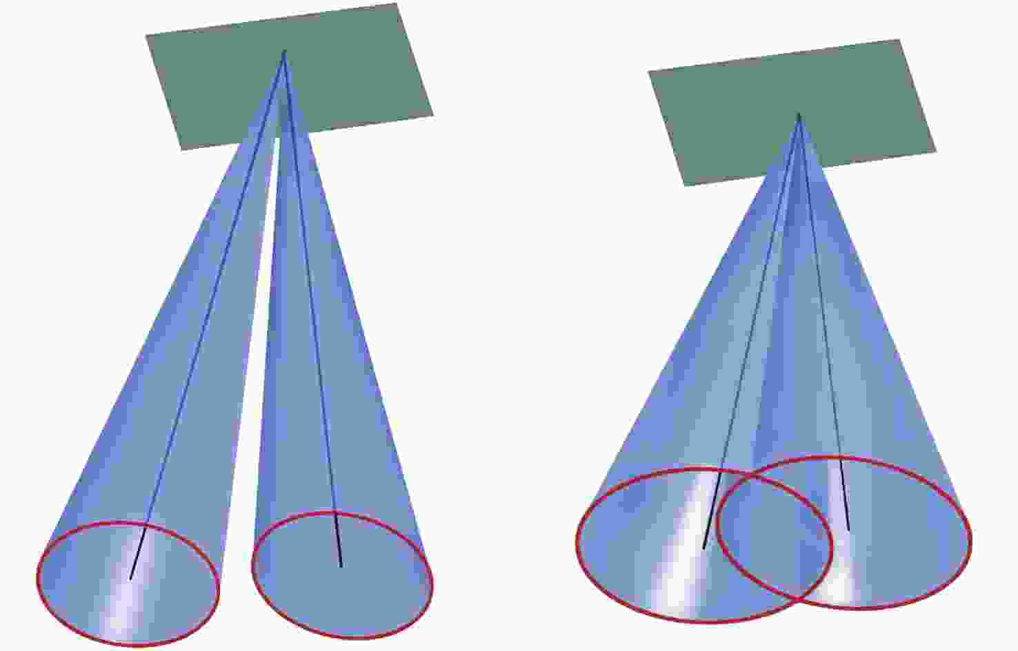
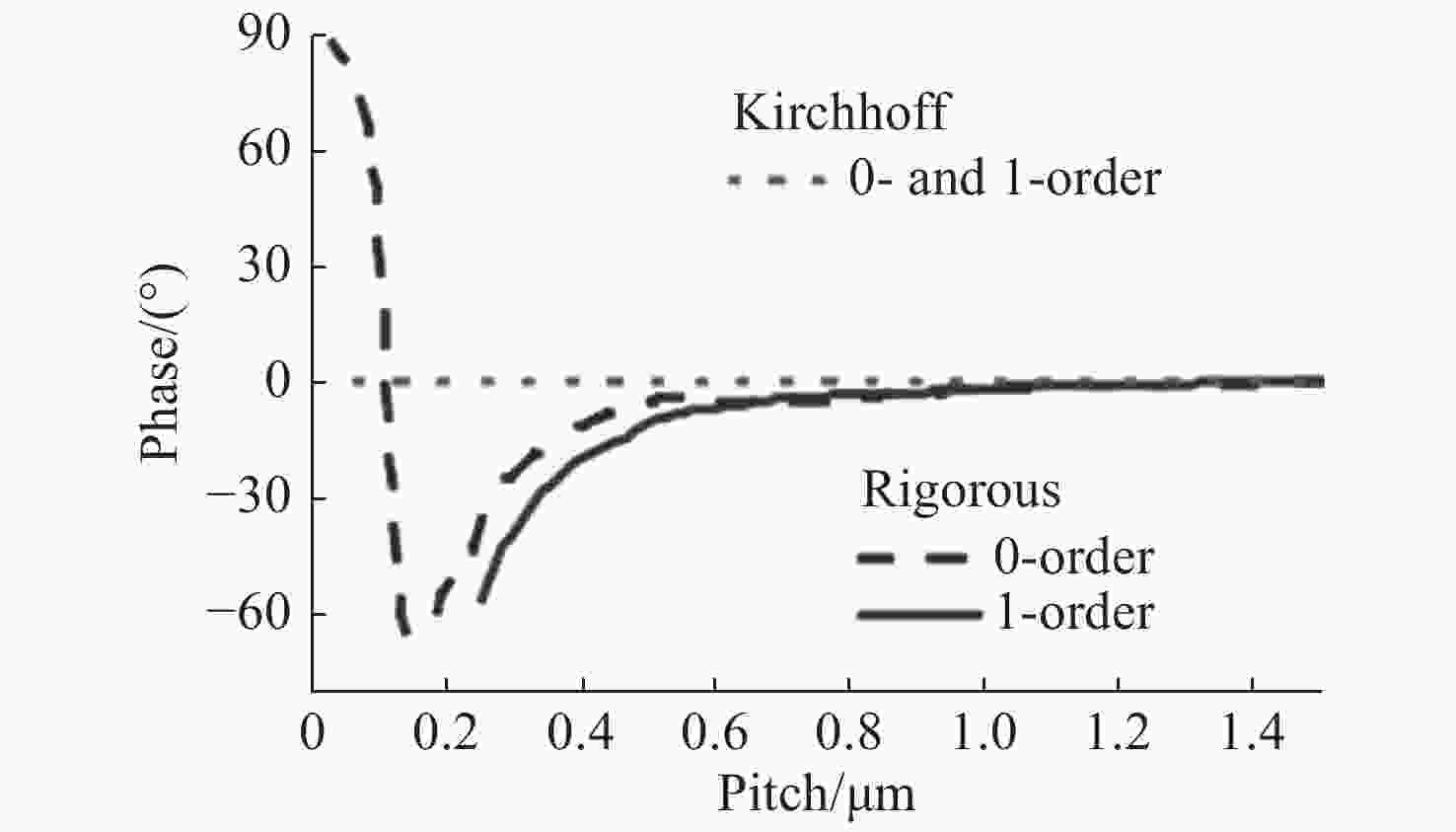
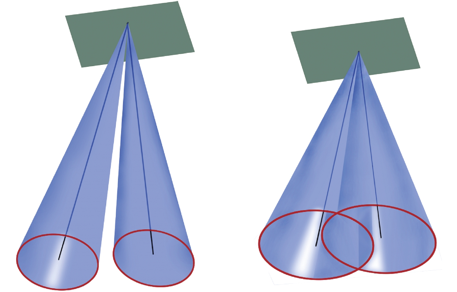
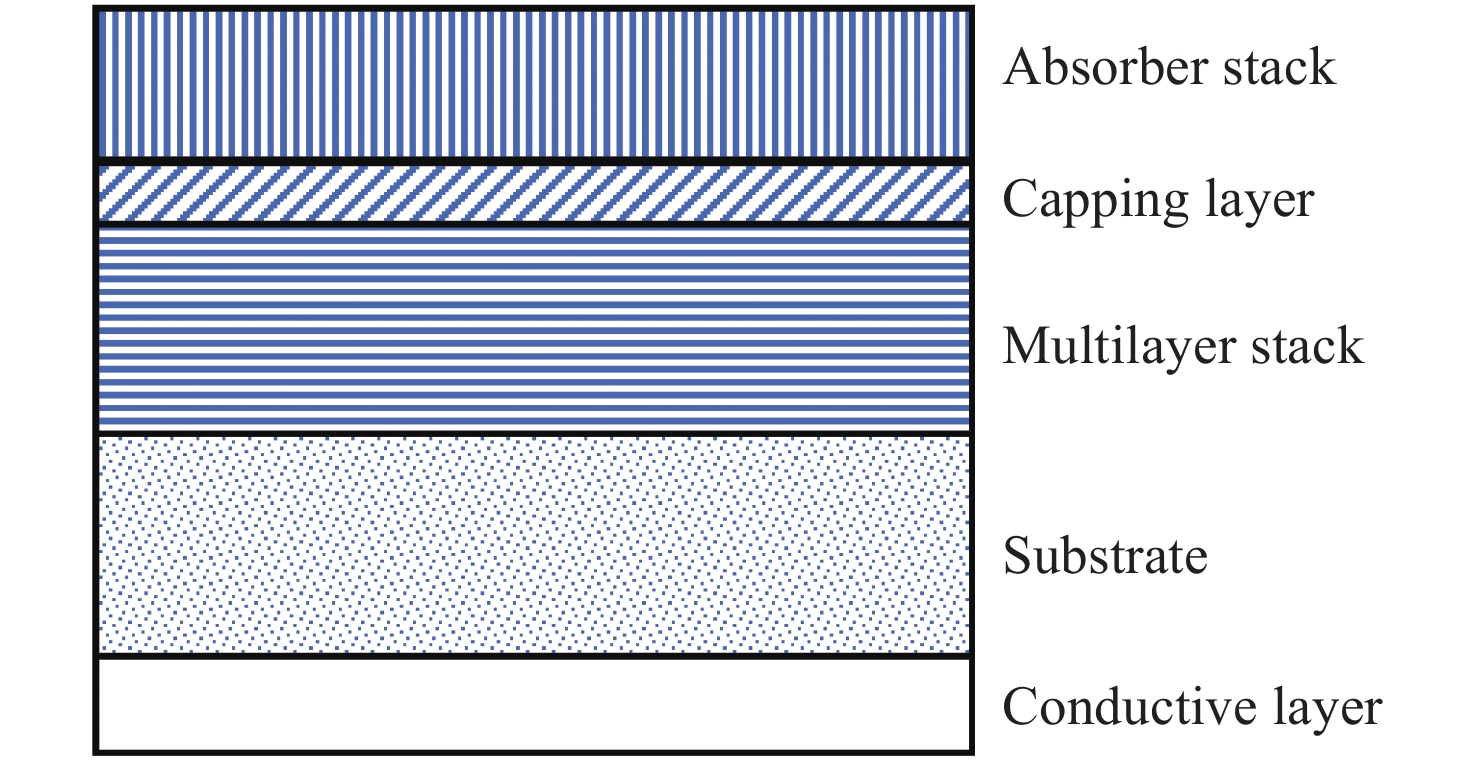
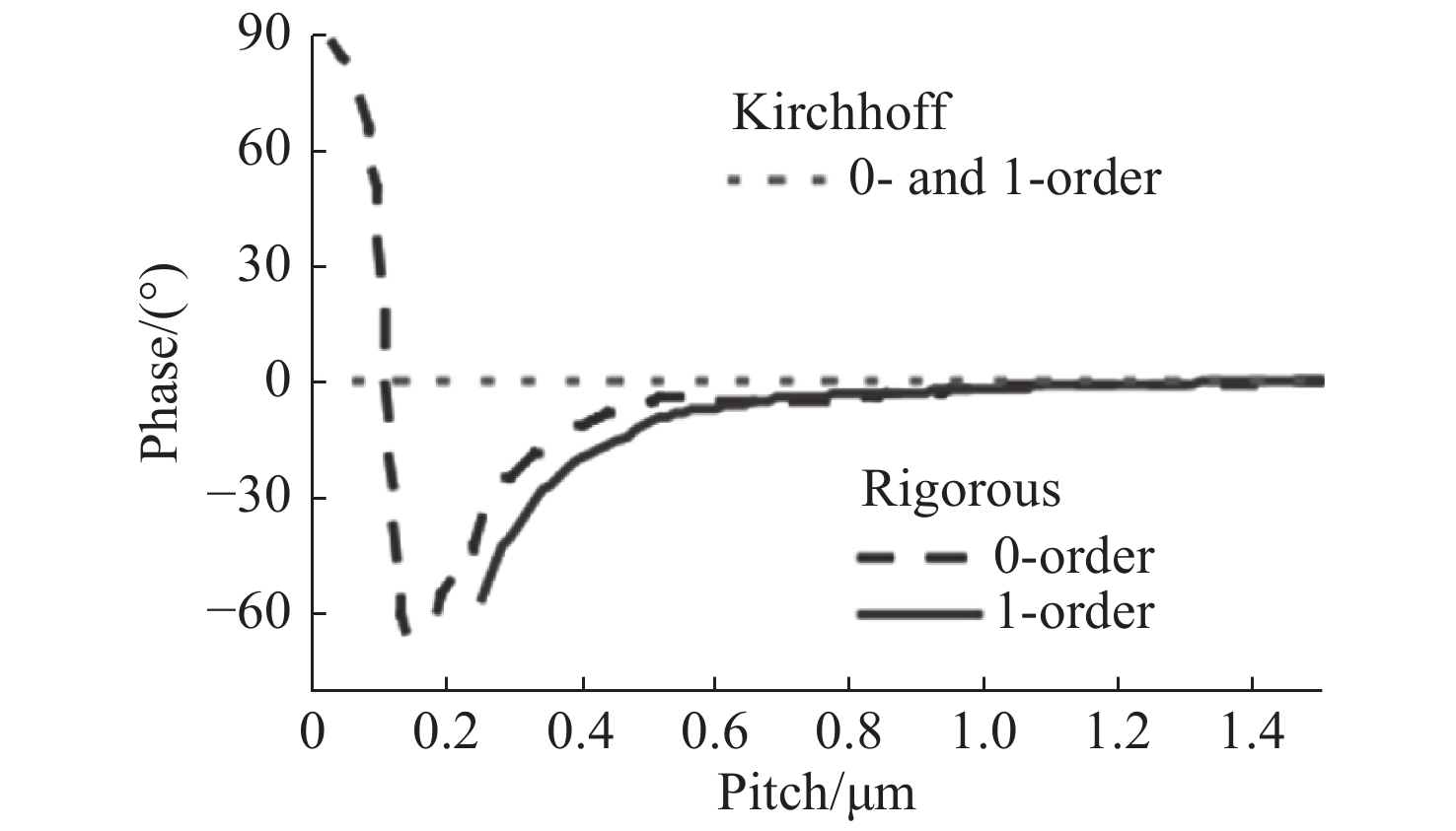
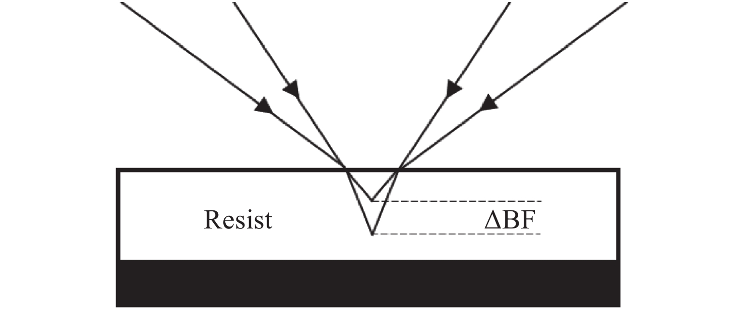
图 3 EUV入射光锥与出射光锥的重叠与不重叠状态
Figure 3. The overlapping and non-overlapping states of the exiting light cone and the incident light cone in EUV
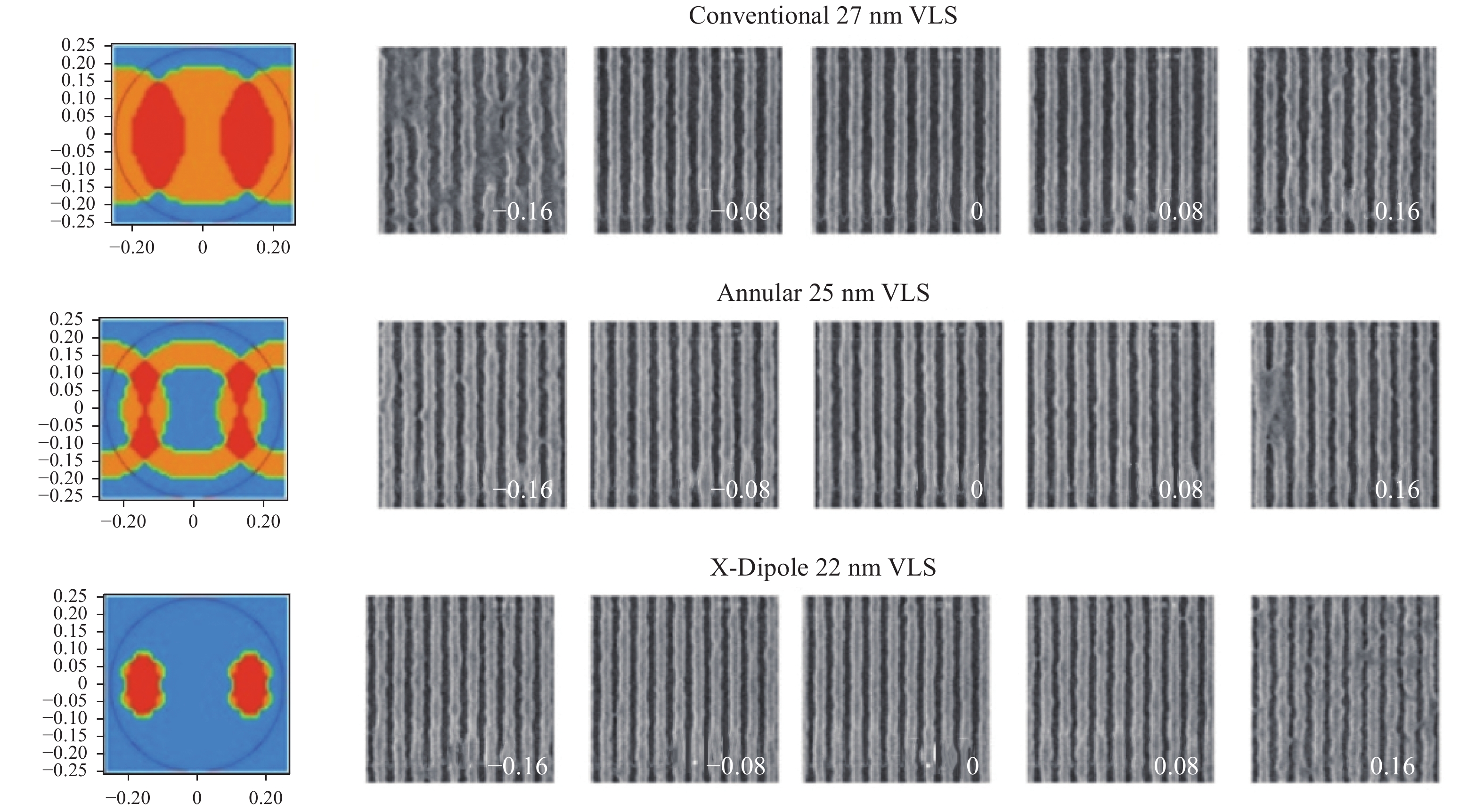
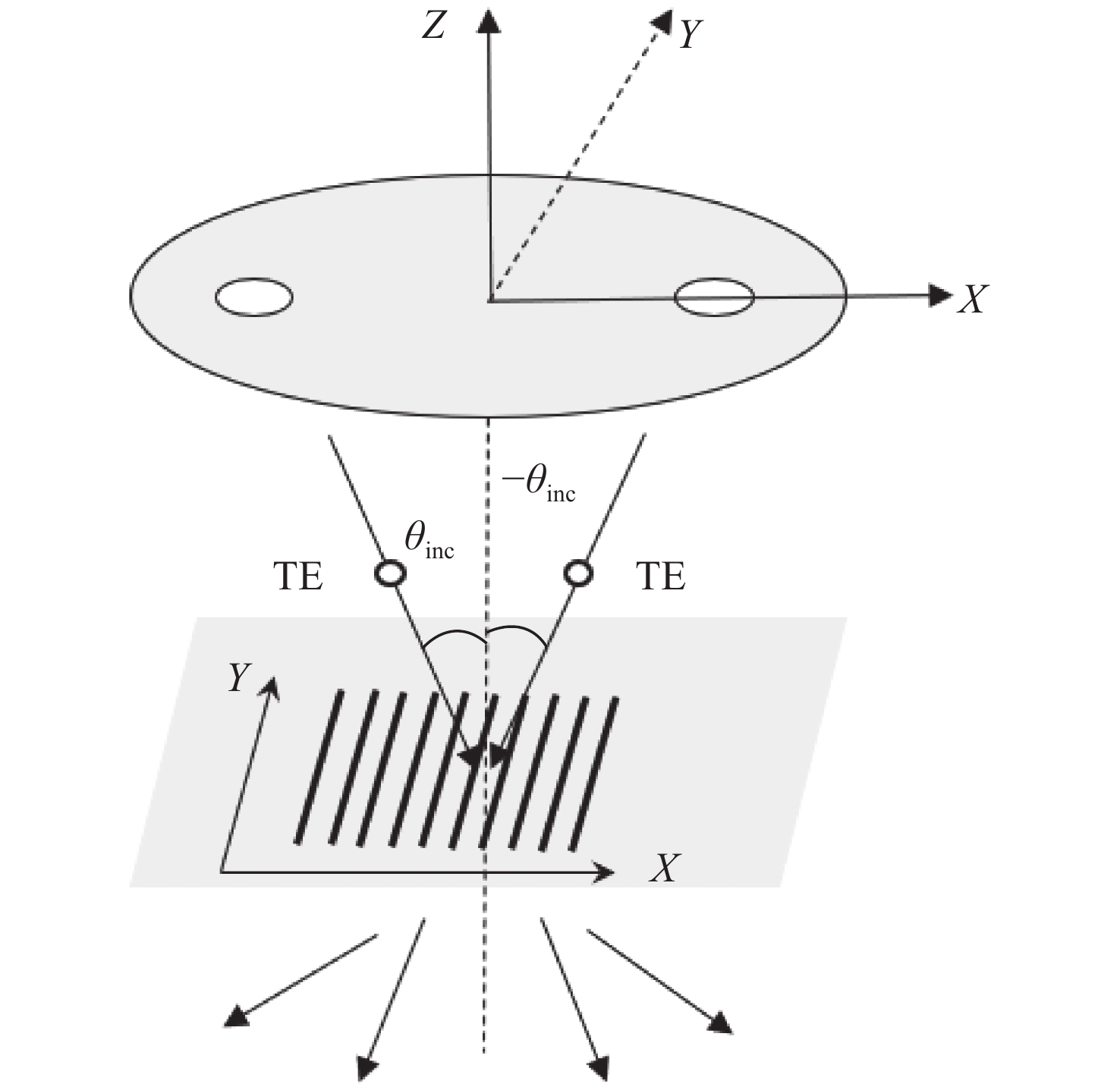
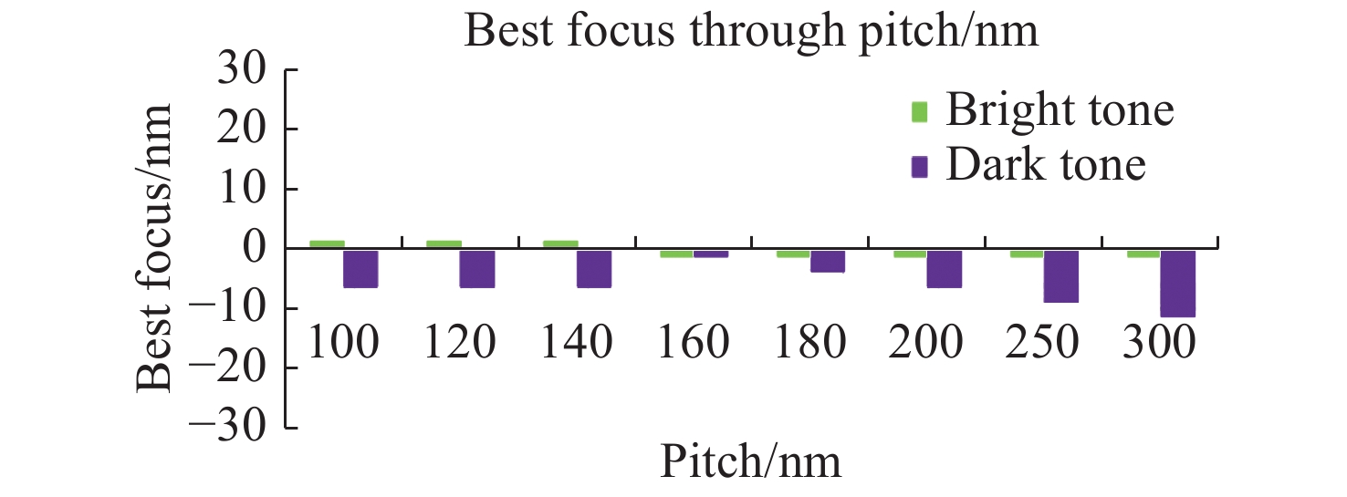
图 5 在双极TE照明下的一维图形(光栅)成像
Figure 5. One-dimensional graphic (grating) imaging under dipole TE illumination

-
[1] China Taiwan Semiconductor Manufacturing Company. TSMC’S 5 nm (FinFET) technology[EB/OL]. [2021-04-17] https://www.tsmc.com/english/dedicatedFoundry/technology/logic/l_5nm. [2] DAN HUTCHESON G. Moore’s law, lithography, and how optics drive the semiconductor industry[J]. Proceedings of SPIE, 2018, 10583: 1058303. [3] 郭杰, 李世光, 赵焱, 等. 电子束硅片图形检测系统中的纳米级对焦控制技术[J]. 中国光学,2019,12(2):242-255. doi: 10.3788/co.20191202.0242GUO J, LI SH G, ZHAO Y, et al. Nano-scale focus control technology in electron beam wafer pattern inspection system[J]. Chinese Optics, 2019, 12(2): 242-255. (in Chinese) doi: 10.3788/co.20191202.0242 [4] 孙裕文, 李世光, 叶甜春, 等. 纳米光刻中调焦调平测量系统的工艺相关性[J]. 光学学报,2016,36(8):0812001. doi: 10.3788/AOS201636.0812001SUN Y W, LI SH G, YE T CH, et al. Process dependency of focusing and leveling measurement system in nanoscale lithography[J]. Acta Optica Sinica, 2016, 36(8): 0812001. (in Chinese) doi: 10.3788/AOS201636.0812001 [5] SHUMWAY J, NEAL N, MEYERS S, et al. Reduction and control of intrafield focus variation on 7nm technology[J]. Proceedings of SPIE, 2018, 10147: 101470B. [6] JANG J H, PARK T, PARK K D, et al. Focus control budget analysis for critical layers of flash devices[J]. Proceedings of SPIE, 2014, 9050: 90502F. [7] 段晨, 宗明成, 范伟, 等. 浸没式光刻机对焦控制技术研究[J]. 光学学报,2018,38(9):0912002. doi: 10.3788/AOS201838.0912002DUAN CH, ZONG M CH, FAN W, et al. Focus control technology in immersion lithography[J]. Acta Optica Sinica, 2018, 38(9): 0912002. (in Chinese) doi: 10.3788/AOS201838.0912002 [8] 姚长呈, 巩岩. 深紫外光刻投影物镜温度特性研究[J]. 中国激光,2016,43(5):0516001. doi: 10.3788/CJL201643.0516001YAO CH CH, GONG Y. Research on temperature distribution of deep ultraviolet lithographic projection objective[J]. Chinese Journal of Lasers, 2016, 43(5): 0516001. (in Chinese) doi: 10.3788/CJL201643.0516001 [9] VAN HAREN R, STEINERT S, MOURAILLE O, et al. The mask contribution as part of the intra-field on-product overlay performance[J]. Proceedings of SPIE, 2018, 11518: 1151813. [10] MASTENBROEK M. EUV industrialization high volume manufacturing with NXE3400B[J]. Proceedings of SPIE, 2018, 10809: 1080904. [11] WAGNER C, HARNED N. Lithography gets extreme[J]. Nature Photonics, 2010, 4(1): 24-26. doi: 10.1038/nphoton.2009.251 [12] 甘雨, 张方, 朱思羽, 等. 光刻机照明系统光瞳特性参数的评估算法[J]. 中国激光,2019,46(3):0304007. doi: 10.3788/CJL201946.0304007GAN Y, ZHANG F, ZHU S Y, et al. Evaluation algorithm of pupil characteristic parameters in lithography illumination system[J]. Chinese Journal of Lasers, 2019, 46(3): 0304007. (in Chinese) doi: 10.3788/CJL201946.0304007 [13] LOWISCH M, KUERZ P, CONRADI Q, et al.. Optics for ASML’s NXE: 3300B platform[C]. Proceedings of SPIE, 2013, 8679: 86791H. [14] HENDRICKX E, GRONHEID R, HERMANS J, et al. Readiness of EUV lithography for insertion into manufacturing: the IMEC EUV program[J]. Journal of Photopolymer Science and Technology, 2013, 26(5): 587-593. doi: 10.2494/photopolymer.26.587 [15] LEE S H, ZHANG ZH Y. Process window study with various illuminations for EUV lithography applications[J]. Proceedings of SPIE, 2007, 6517: 65172P. doi: 10.1117/12.713447 [16] MACK C, CHICHESTER W. Fundamental Principles of Optical Lithography: the Science of Microfabrication[M]. Chichester: Wiley, 2008: 60. [17] ZHAI A P, CAO Y P, CHEN B, et al. A novel method of partial coherence measuring for the illumination system and its defocus performance analysis[J]. Optik, 2013, 124(23): 6313-6317. doi: 10.1016/j.ijleo.2013.06.009 [18] DE SIMONE D, KLJUCAR L, DAS P, et al. 28 nm pitch single exposure patterning readiness by metal oxide resist on 0.33 NA EUV lithography[J]. Proceedings of SPIE, 2021, 11609: 116090Q. [19] KNEER B, MIGURA S, KAISER W, et al. EUV lithography optics for sub-9 nm resolution[J]. Proceedings of SPIE, 2015, 9422: 94221G. doi: 10.1117/12.2175488 [20] CONLEY W, ALAGNA P, SHIEH J, et al. The impact of lower light source bandwidth on sub-10 nm process node features[J]. Proceedings of SPIE, 2017, 10147: 1014707. [21] RUOFF V D M J, NEUMANN J T, SCHMITT-WEAVER E, et al. Polarization-induced astigmatism caused by topographic masks[J]. Proceedings of SPIE, 2007, 6730: 67301T. [22] TANABE H, SATO S, TAKAHASHI A. Fast 3D lithography simulation by convolutional neural network[J]. Proceedings of SPIE, 2020, 11518: 115180L. [23] HAO Y Y, LI Y Q, LI T, et al. The calculation and representation of polarization aberration induced by 3D mask in lithography simulation[J]. Proceedings of SPIE, 2017, 10460: 104601J. [24] 韦亚一. 超大规模集成电路先进光刻理论与应用[M]. 北京: 科学出版社, 2016: 103-105.WEI Y Y. Advanced Lithography Theory and Application for VLSI[M]. Beijing: Science Press, 2016: 103-105. (in Chinese) [25] AZPIROZ J T, ROSENBLUTH A E. Impact of sub-wavelength electromagnetic diffraction in optical lithography for semiconductor chip manufacturing[C]. Proceedings of the 2013 SBMO/IEEE MTT-S International Microwave & Optoelectronics Conference, IEEE, 2013: 1-5. [26] SAIED M, FOUSSADIER F, BELLEDENT J, et al. Three-dimensional mask effects and source polarization impact on OPC model accuracy and process window[J]. Proceedings of SPIE, 2007, 6520: 65204Q. doi: 10.1117/12.715120 [27] YAN P Y. Understanding Bossung curve asymmetry and focus shift effect in EUV lithography[J]. Proceedings of SPIE, 2002, 4562: 279-287. doi: 10.1117/12.458302 [28] ERDMANN A. Topography effects and wave aberrations in advanced PSM technology[J]. Proceedings of SPIE, 2001, 4346: 345. doi: 10.1117/12.435734 [29] BURKHARDT M, RAGHUNATHAN A. Best focus shift mechanism for thick masks[J]. Proceedings of SPIE, 2015, 9422: 94220X. [30] NAKAJIMA Y, SATO T, INANAMI R, et al. Aberration budget in extreme ultraviolet lithography[J]. Proceedings of SPIE, 2008, 6921: 69211A. [31] ERDMANN A, EVANSCHITZKY P, FÜHNER T. Mask diffraction analysis and optimization for EUV masks[J]. Proceedings of SPIE, 2009, 7271: 72711E. [32] ERDMANN A, EVANSCHITZKY P, NEUMANN J T, et al. Mask-induced best-focus shifts in deep ultraviolet and extreme ultraviolet lithography[J]. Journal of Micro/Nanolithography, 2016, 15(2): 021205. doi: 10.1117/1.JMM.15.2.021205 [33] HAQUE R R, LEVINSON Z, SMITH B W. 3D mask effects of absorber geometry in EUV lithography systems[J]. Proceedings of SPIE, 2016, 9776: 97760F. [34] MOCHI I, PHILIPSEN V, GALLAGHER E, et al. Assist features: placement, impact, and relevance for EUV imaging[J]. Proceedings of SPIE, 2016, 9776: 97761S. doi: 10.1117/12.2220025 [35] BOUMA A, MIYAZAKI J, VAN VEEN M, et al. Impact of mask absorber and quartz over-etch on mask 3D induced best focus shifts[J]. Proceedings of SPIE, 2014, 9231: 92310S. doi: 10.1117/12.2068155 [36] SZUCS A, PLANCHOT J, FARYS V, et al. Best focus shift mitigation for extending the depth of focus[J]. Proceedings of SPIE, 2013, 8683: 868313. doi: 10.1117/12.2011114 [37] INOUE S, ITOH M, ASANO M, et al. Desirable reticle flatness from focus deviation standpoint in optical lithography[J]. Journal of Micro/Nanolithography,MEMS,and MOEMS, 2002, 1(3): 307. doi: 10.1117/1.1503806 [38] LIU P, XIE X B, LIU W, et al. Fast 3D thick mask model for full-chip EUVL simulations[J]. Proceedings of SPIE, 2013, 8679: 86790W. doi: 10.1117/12.2010818 [39] SEARS M K, SMITH B W. Modeling the effects of pupil-manipulated spherical aberration in optical nanolithography[J]. Journal of Micro/Nanolithography,MEMS,and MOEMS, 2013, 12(1): 013008. doi: 10.1117/1.JMM.12.1.013008 [40] BRUNNER T A. Impact of lens aberrations on optical lithography[J]. IBM Journal of Research and Development, 1997, 41(1-2): 57-67. [41] BEKAERT J, VAN LOOK L, VANDENBERGHE G, et al. Characterization and control of dynamic lens heating effects under high volume manufacturing conditions[J]. Proceedings of SPIE, 2011, 7973: 79730V. doi: 10.1117/12.881609 [42] LEVINSON H J. Principles of Lithography[M]. 3rd ed. Bellingham, WA: SPIE Press, 2011: 40-41. [43] 李艳秋, 刘岩, 刘丽辉. 16 nm极紫外光刻物镜热变形对成像性能影响的研究[J]. 光学学报,2019,39(1):0122001. doi: 10.3788/AOS201939.0122001LI Y Q, LIU Y, LIU L H. Effect of thermal deformation on imaging performance for 16 nm extreme ultraviolet lithography objective[J]. Acta Optica Sinica, 2019, 39(1): 0122001. (in Chinese) doi: 10.3788/AOS201939.0122001 [44] SEARS M K, BEKAERT J, SMITH B W. Lens wavefront compensation for 3D photomask effects in subwavelength optical lithography[J]. Applied Optics, 2013, 52(3): 314-322. doi: 10.1364/AO.52.000314 [45] HO G H, CHENG A, CHEN CH J, et al. Lens-heating-induced focus drift of I-line step and scan: correction and control in a manufacturing environment[J]. Proceedings of SPIE, 2001, 4344: 289-296. doi: 10.1117/12.436722 [46] 王帆, 王向朝, 马明英, 等. 光刻机投影物镜像差的现场测量技术[J]. 激光与光电子学进展,2004,41(6):33-37.WANG F, WANG X ZH, MA M Y, et al. In-situ measurement methods of lens aberration[J]. Laser &Optoelectronics Progress, 2004, 41(6): 33-37. (in Chinese) [47] CUI Y T. Fine-tune lens-heating-induced focus drift with different process and illumination settings[J]. Proceedings of SPIE, 2001, 4346: 1369-1378. doi: 10.1117/12.435675 [48] CHANG Y S, WU M J, HUNG M Y, et al. Polygate within wafer CD uniformity improvement by the minimization of lens heating effect[J]. Proceedings of SPIE, 2001, 4404: 26-32. doi: 10.1117/12.425219 [49] CHENG B J, LIU H CH, CUI Y T, et al. Improving image control by correcting the lens-heating focus drift[J]. Proceedings of SPIE, 2000, 4000: 818-826. doi: 10.1117/12.389075 [50] LEE S H, SHROFF Y, CHANDHOK M. Flare and lens aberration requirements for EUV lithographic tools[J]. Proceedings of SPIE, 2005, 5751: 707-714. doi: 10.1117/12.604870 [51] MONTCALM C, BAJT S, MIRKARIMI P B, et al. Multilayer reflective coatings for extreme-ultraviolet lithography[J]. Proceedings of SPIE, 1998, 3331: 42-51. doi: 10.1117/12.309600 [52] FINDERS J. The impact of Mask 3D and Resist 3D effects in optical lithography[J]. Proceedings of SPIE, 2014, 9052: 905205. [53] PENG A, HSU S D, HOWELL R C, et al. Lithography-defect-driven source-mask optimization solution for full-chip optical proximity correction[J]. Applied Optics, 2021, 60(3): 616-620. doi: 10.1364/AO.408405 [54] LIU X F, HOWELL R, HSU S, et al. EUV source-mask optimization for 7nm node and beyond[J]. Proceedings of SPIE, 2014, 9048: 90480Q. doi: 10.1117/12.2047584 [55] WU Q. Key points in 14 nm photolithographic process development, challenges and process window capability[C]. Proceedings of 2017 China Semiconductor Technology International Conference, IEEE, 2017: 1-6. [56] JIA N N, YANG S H, KIM S, et al. Study of lens heating behavior and thick mask effects with a computational method[J]. Proceedings of SPIE, 2014, 9052: 905209. [57] 王丽萍. 长春光机所承担的国家科技重大专项项目“极紫外光刻关键技术研究”通过验收[J]. 分析仪器,2017(4):96.WANG L P. The project of “study of key technology for extreme-ultraviolet lithography” passed the acceptance inspection[J]. Analytical Instrumentation, 2017(4): 96. (in Chinese) [58] DENG X J, CHAO A, FEIKES J, et al. Experimental demonstration of the mechanism of steady-state microbunching[J]. Nature, 2021, 590(7847): 576-579. doi: 10.1038/s41586-021-03203-0 -

 下载:
下载:


图(18)
计量
- 文章访问数: 5540
- HTML全文浏览量: 2965
- PDF下载量: 576
- 被引次数: 0
