


-
摘要: 传统光学透镜及光学系统基于光传播效应实现电磁波调控功能,其体积较大、不易集成。而超表面是由人工亚波长尺度单元构成的二维平面结构,由于其相对于传统透镜具有超薄的优势,并且可以实现对光场的任意调控,近年来在光学成像领域得到广泛研究和应用。本文阐述了超表面透镜的工作原理,分析了超表面成像透镜的单色像差和色像差成因以及对应的像质评价方法,之后综述了超表面成像透镜的研究现状及应用,最后总结了超表面在成像领域尚且存在的问题及其未来发展方向。超表面透镜便于集成、设计自由度高,有望在诸多应用领域取代传统成像器件,基于超表面的高效率、大视场、宽带、可重构可调谐成像器件将成为其未来重要发展方向。Abstract: Traditional optical lenses and optical systems implement electromagnetic wave control based on the light propagation effect. So they usually suffer from the bulky size. Recently, metasurfaces comprised of artificial subwavelength structures have been widely studied, since they take great advantages of their subwavelength thickness and provide arbitrary control of electromagnetic waves. Here, the electromagnetic wave control mechanism is introduced. Then, we analyze the monochromatic aberrations and chromatic aberrations of the metalens and the corresponding image quality evaluation methods. Also, we discuss the research progress and applications of metalens for imaging. The exist problems and future goals are pointed out at the end of the review. Based on the advantages of portability and a high degree of design freedom, metalens are expected to replace the traditional imaging devices in many applications. High efficiency, large field of view, broadband, reconfigurable and tunable imaging devices based on metasurfaces will help in important future development directions.
-
Key words:
- metasurface /
- imaging /
- electromagnetic wave manipulation /
- aberration /
- image evaluation
-
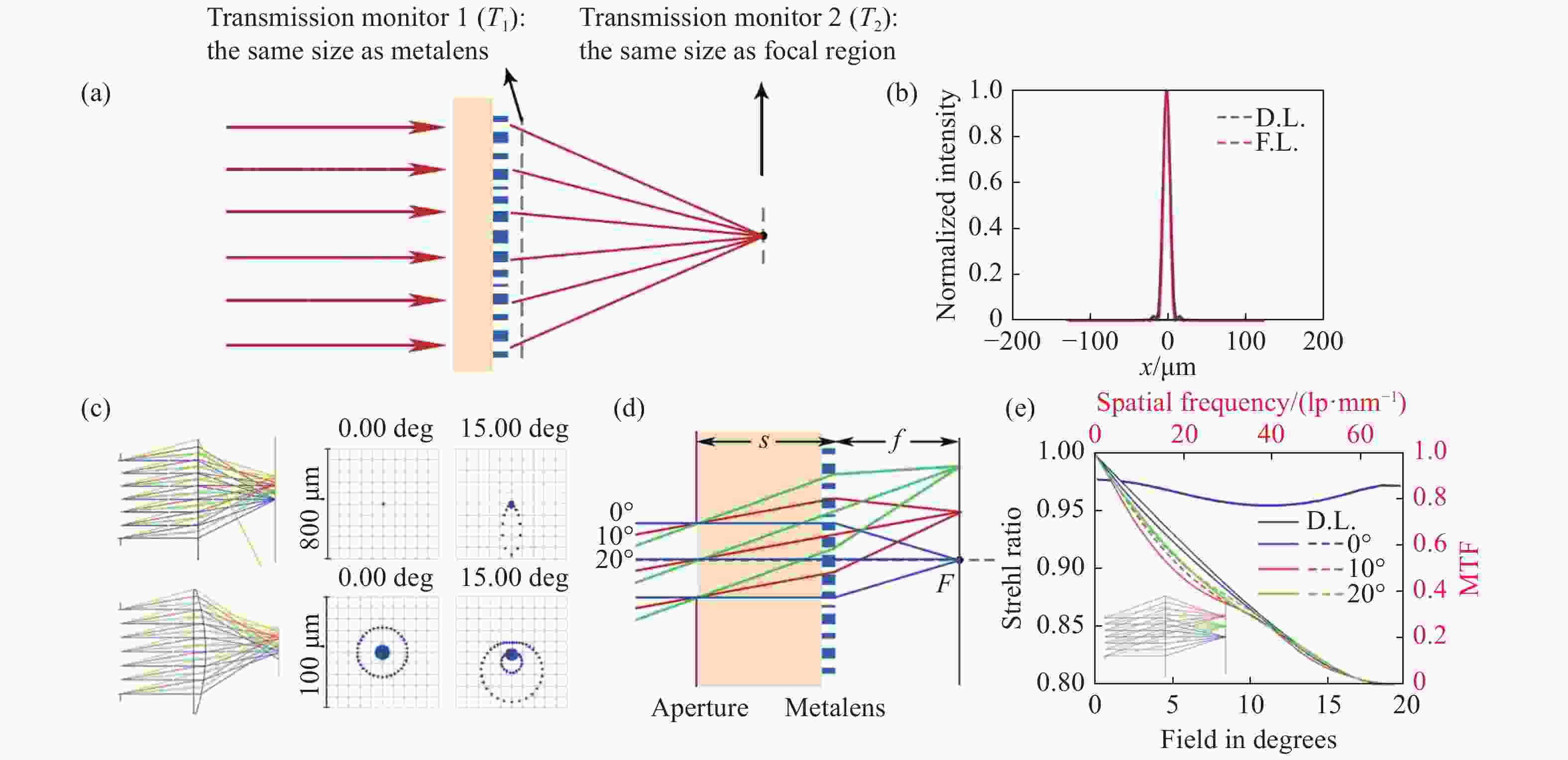
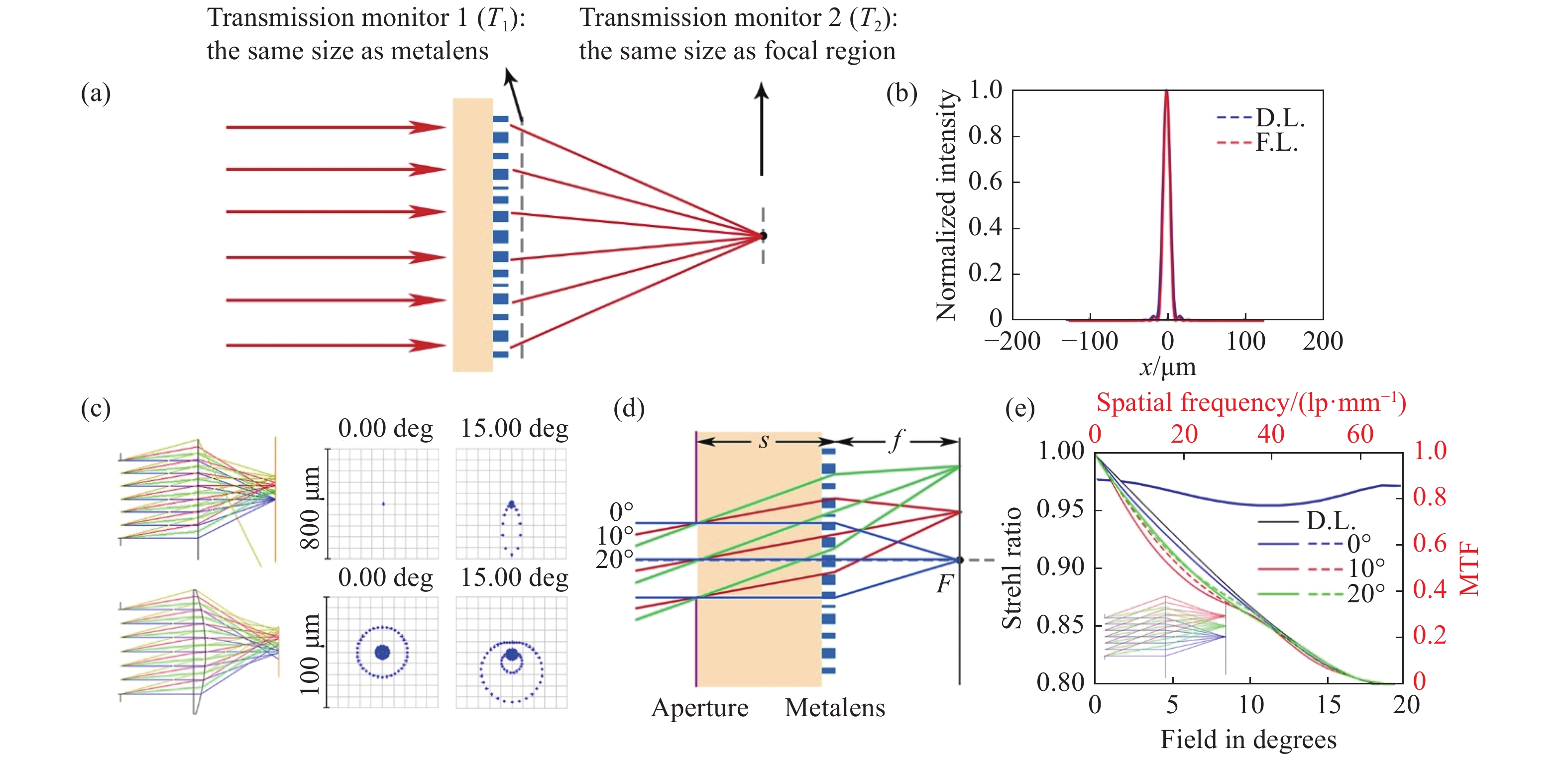
图 1 超表面透镜像差分析。(a)聚焦效率计算示意图。(b)超表面透镜焦平面电场分布图,其中蓝色、红色曲线分别代表衍射极限下的焦平面电场分布和超表面会聚透镜焦平面电场分布。(c)双曲相位分布衍射平面(上)和传统球面单透镜(下)的光学系统示意图及其对应的点列图。(d)消轴外像差超表面透镜结构。(e)衍射光学元件的斯特列尔比分布及不同入射角下的调制传递函数(MTF)。
Figure 1. The aberration analysis of metalens. (a) The schematic of focusing efficiency calculation. (b) The vertical cut of the focal spot of the metalens. The blue line and the red line represent the diffraction-limited intensity profile and the intensity profile of focusing metalens, respectively. (c) The schematics optical system and spot diagrams of metalens with hyperbolic phase profile (top) and traditional spherical lens (bottom). (d) The schematic of metalens designed for off-axis aberration correction. (e) The Strehl ratio and the Modulation Transfer Function (MTF) of the diffractive optical elements at different incidence angles.
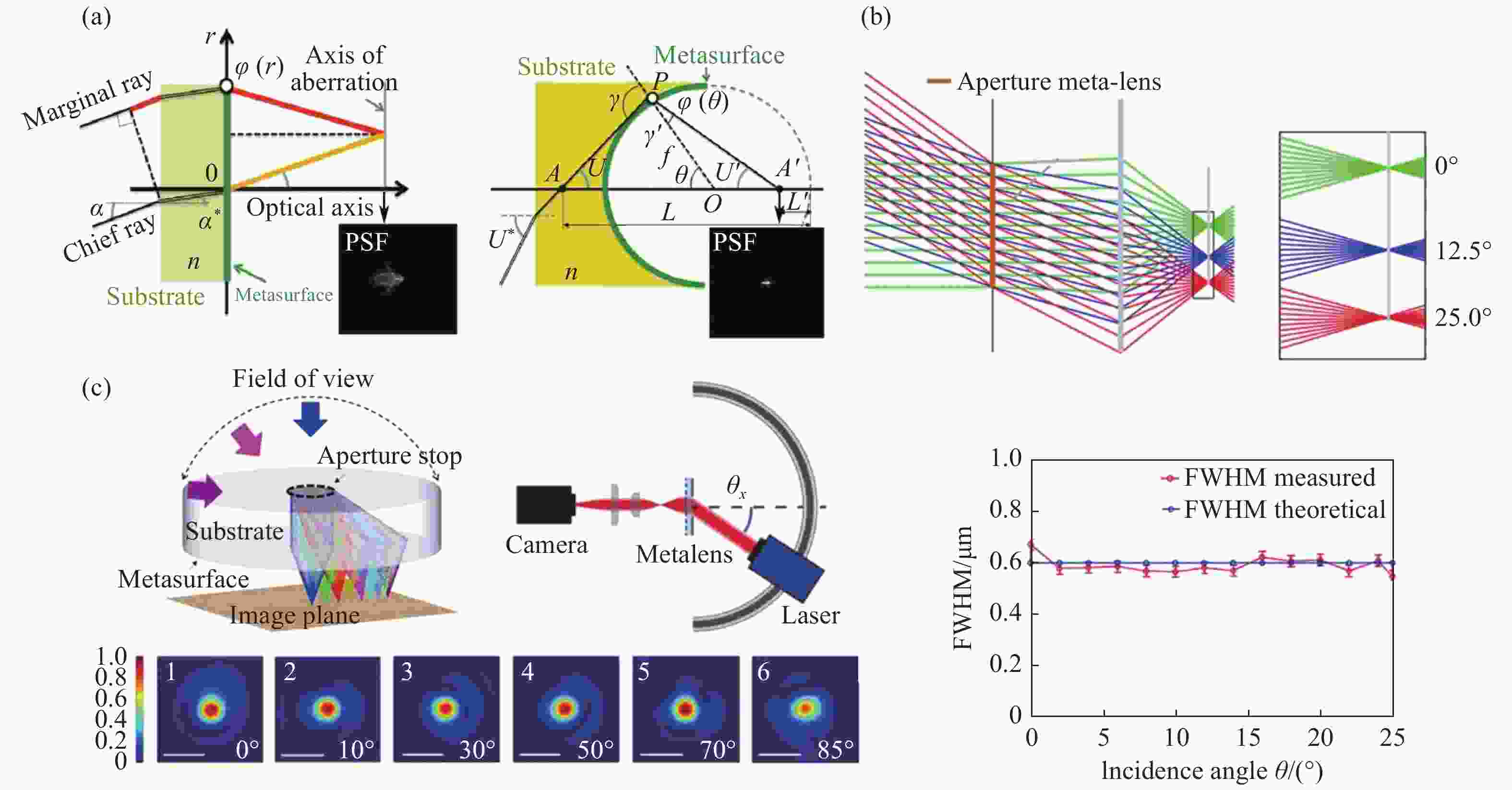
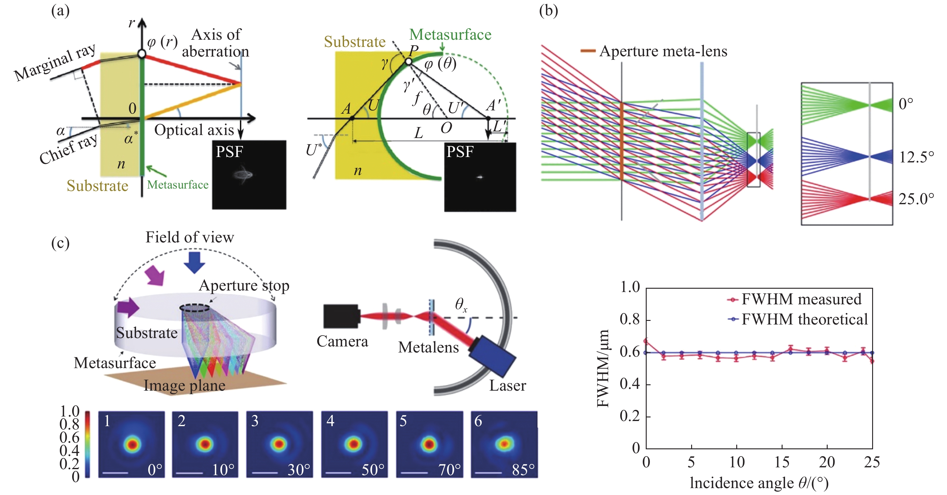
图 2 消轴外像差超表面透镜设计。(a)平面超表面透镜(左)和弯曲基板超表面透镜(右)示意图及二者在中心波长1.55 μm、入射角10°条件下的点列图(PSF)[46]。(b)级联透镜校正剩余球差原理示意图(上)及不同角度入射光下级联透镜聚焦光斑的FWHM测量值(下)[58]。(c)超大视场角单层平面超表面透镜示意图(左上)、用于测量不同入射角下聚焦光斑的实验装置示意图(右上)和不同角度入射光下的聚焦光斑测量结果(下)[59]。
Figure 2. Metalens designs for monochromatic aberration correction. (a) Schematics and Point Spread Function (PSF) of a flat lens (left) and an aplanatic metasurface (right) illuminated with parallel monochromatic light at λ=1.55 μm and incident at an angle α=10°[46]. [Reprinted/Adapted] with permission from [ref. 46] © The Optical Society. (b) The operation of the metalens doublet in terms of the correction of spherical aberration (top) and measured FWHM of focal spot intensity profiles at different incident angle θ (bottom)[58]. Reprinted (adapted) with permission from (GROEVER B, CHEN W T, CAPASSO F. Meta-Lens Doublet in the Visible Region[J]. Nano Letters, 2017, 17(8):4902-4907.). Copyright (2017) American Chemical Society. (c) Schematic of a single-layer planar metalens with an ultra-wide FOV (top-left), schematic of experimental setup for imaging a focal spot produced by metasurface at various incident angles (top-right) and measured focusing spots at all incident angles (bottom)[59]. Reprinted (adapted) with permission from (SHALAGINOV M Y, AN S, YANG F, et al.. Single-Element Diffraction-Limited Fisheye Metalens[J]. Nano Letters, 2020, 20(10):7429-7437.). Copyright (2020) American Chemical Society.
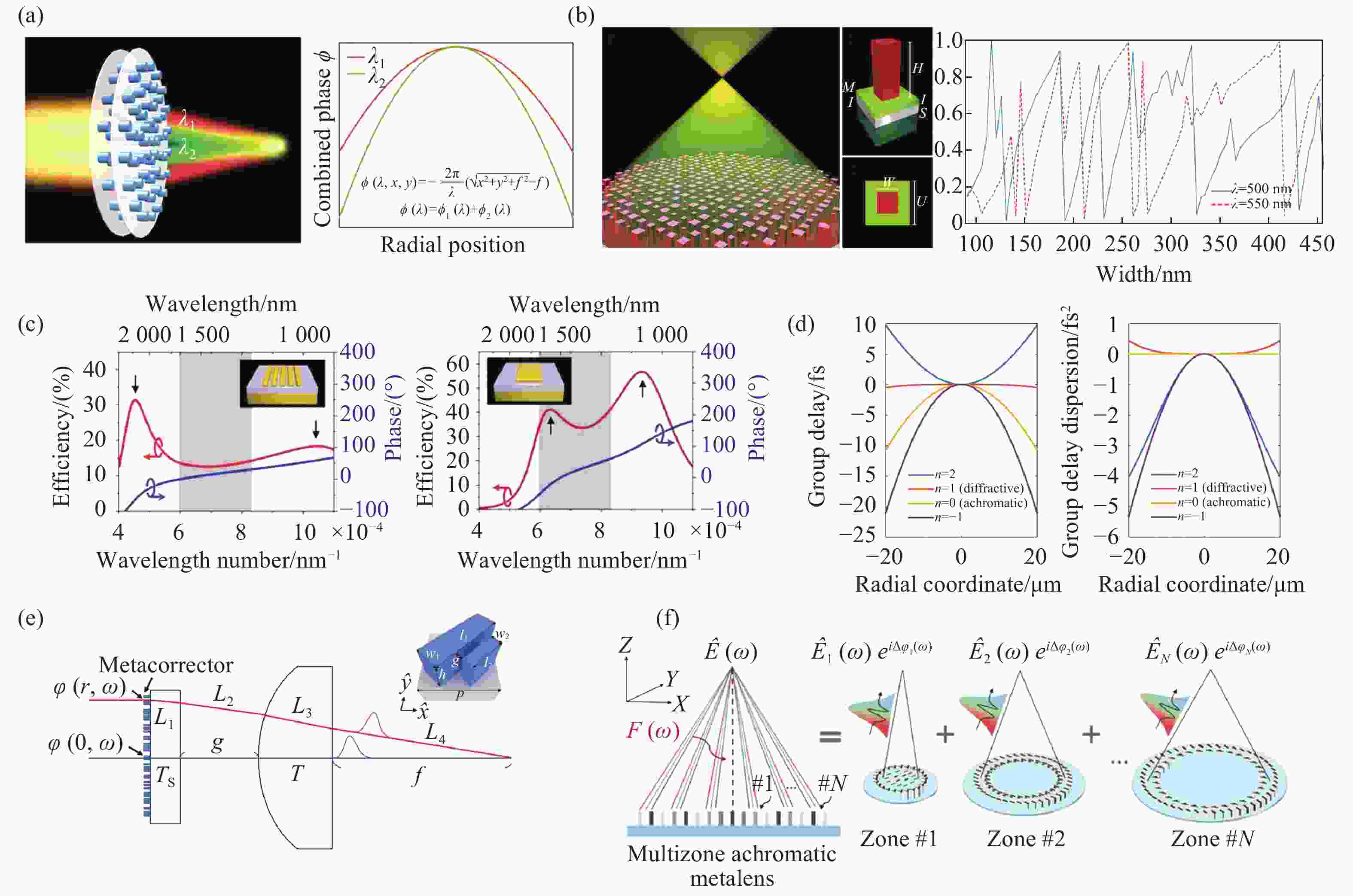
图 3 消色差超表面透镜设计。(a)将两个不同波长的光聚焦在同一位置的超表面级联透镜示意图。每层超表面的相位共同提供了两个不同波长下所需的双曲线相位分布[62]。(b)反射式消色差超表面透镜示意图(左)以及工作波长500 nm和550 nm下反射光附加相位与纳米柱宽度的关系(右)[64]。(c)两种集成谐振单元的偏振转换效率(红色)和相位分布(蓝色)图[42]。(d)不同色散特性超表面透镜所需的相对群延迟和相对群延迟色散分布。(e)由超表面校正透镜和传统球面镜构成的光学系统示意图[67]。(f)分区消色差超表面透镜示意图[69]。
Figure 3. Metalens designs for chromatic aberration correction. (a) Schematic diagram of a metasurface cascade lens that focuses two different wavelengths of light at the same position. The phases at each layer together to provide the required hyperbolic phase profiles at the two different wavelengths[62]. Reprinted (adapted) with permission from (ZHOU Y, KRAVCHENKO I I, WANG H, et al.. Multilayer Noninteracting Dielectric Metasurfaces for Multiwavelength Metaoptics[J]. Nano Letters, 2018, 18(12):7529-7537.). Copyright (2018) American Chemical Society. (b) Schematic of an achromatic metalens working in reflection mode (left). Computed reflection phase shift as a function of the nanopillar width at two different wavelength of 500 and 550 nm (right)[64]. Reprinted (adapted) with permission from (KHORASANINEJAD M, SHI Z, ZHU A Y, et al.. Achromatic Metalens over 60 nm Bandwidth in the Visible and Metalens with Reverse Chromatic Dispersion[J]. Nano Letters, 2017, 17(3):1819-1824.). Copyright (2017) American Chemical Society. (c) Polarization conversion efficiency (red curves) and phase profile (blue curves) for integrated-resonant unit elements (IRUEs)[42]. Reprinted (adapted) with permission from (WANG S, WU P C, SU V-C, et al.. A broadband achromatic metalens in the visible[J]. Nature Nanotechnology, 2018, 13(3):227-232.). Copyright (2017) Shuming Wang et al. (d) Required relative group delays (left) and relative group delay dispersion (right) as a function of metalens coordinate. (e) Schematic of a hybrid lens consisting of a metacorrector and a spherical lens[67]. Reprinted (adapted) with permission from (CHEN W T, ZHU A Y, SISLER J, et al.. Broadband Achromatic Metasurface-Refractive Optics[J]. Nano Letters, 2018, 18(12):7801-7808.). Copyright (2018) American Chemical Society. (f) Schematic drawing of a multizone RGB-achromatic metalens showing achromatic focusing of RGB light coming from different lens locations[69]. From [LI Z, LIN P, HUANG Y-W, et al.. Meta-optics achieves RGB-achromatic focusing for virtual reality[J]. Science Advances, 2021, 7(5):eabe4458.]. Reprinted with permission from AAAS.
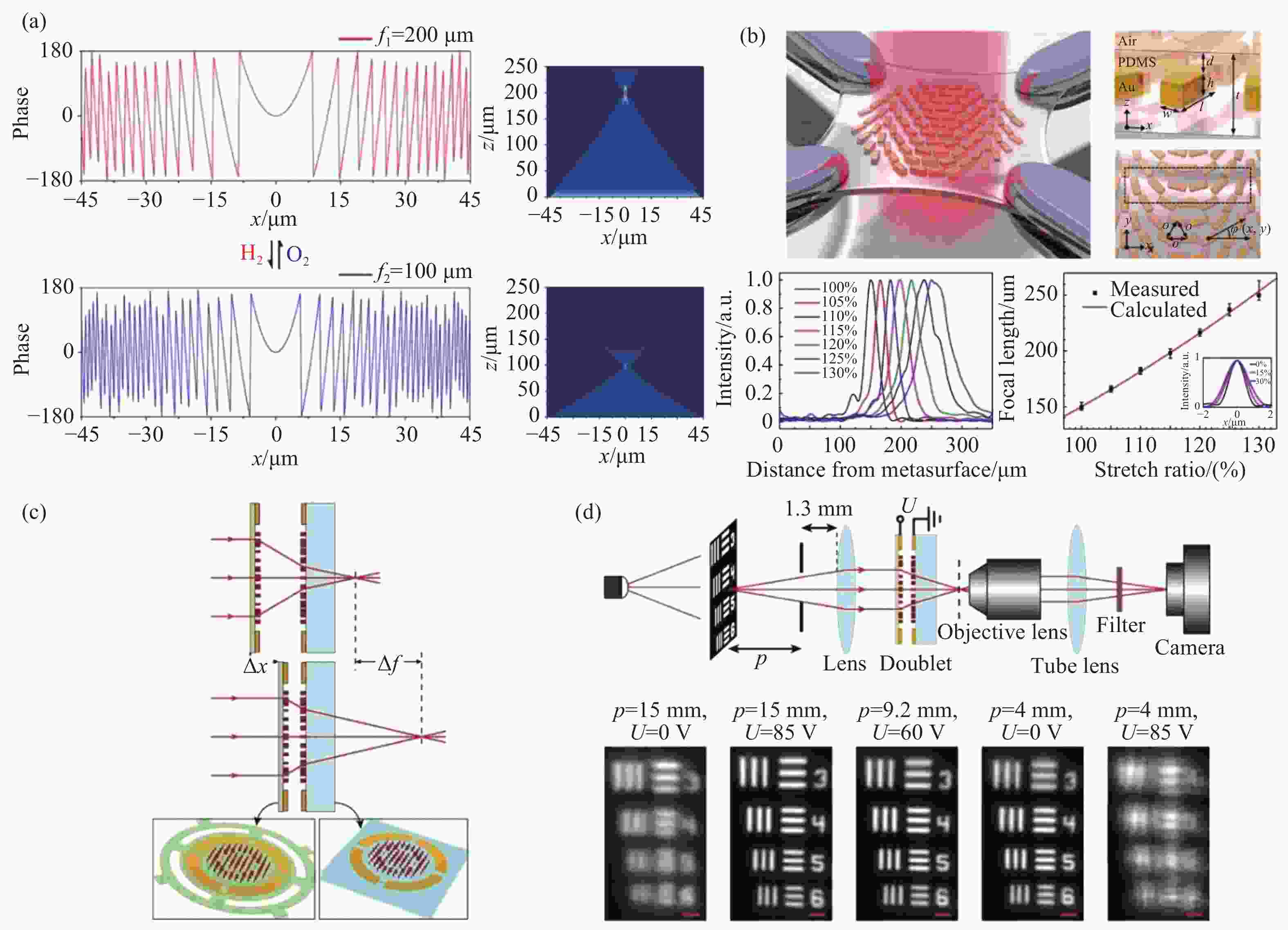
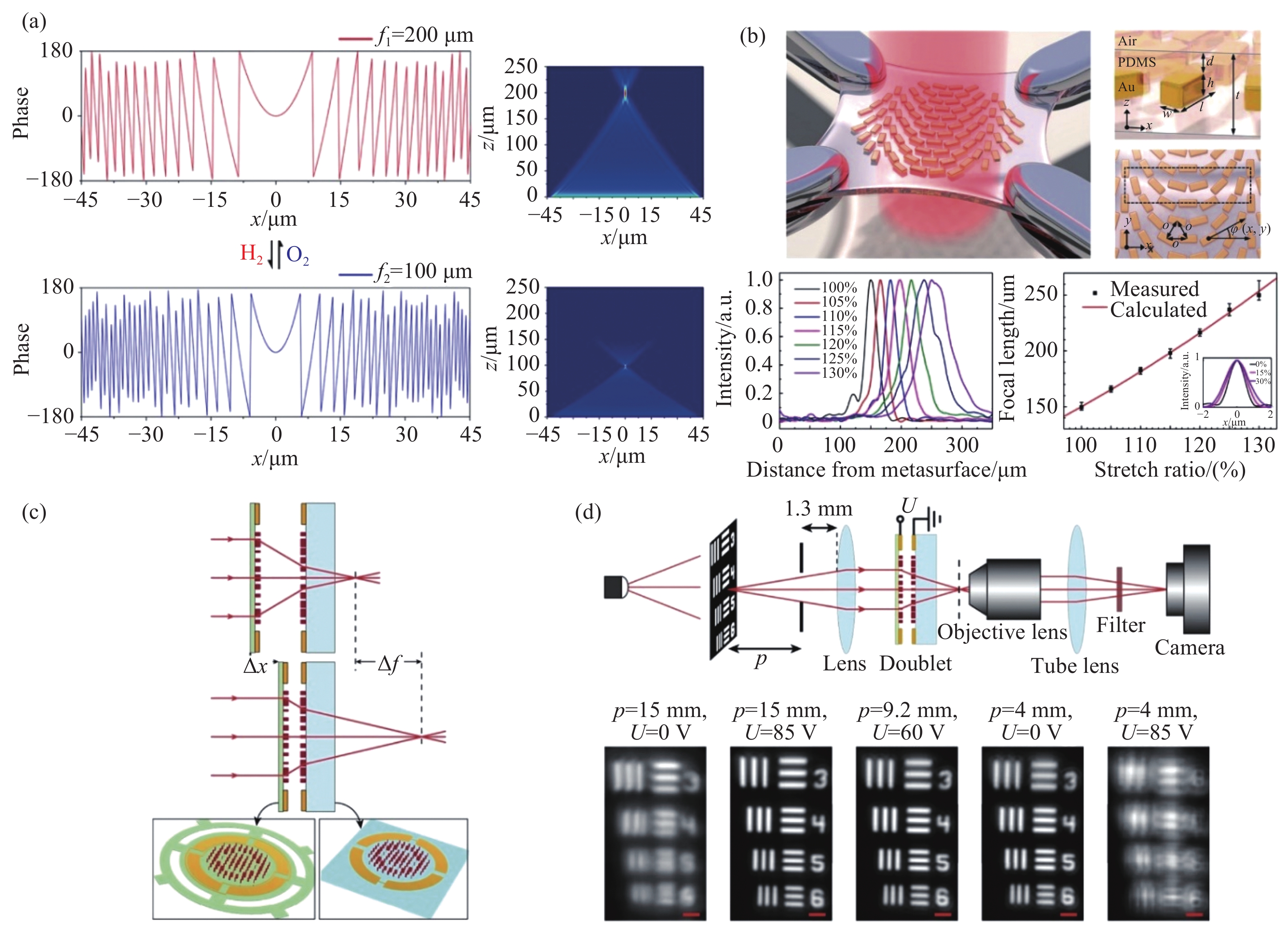
图 4 可调及可重构超表面透镜设计。(a)氢化反应前后超表面透镜的相位分布以及对应的电场强度分布[89]。(b)可拉伸PDMS衬底超表面示意图(上),纳米棒的长、宽、高以及埋入深度分别为l=240 nm, w=100 nm, h=70 nm, and d=200 nm。不同拉伸比s对应的透射圆偏振光沿光轴的强度分布(左下)以及焦距测量值和计算值(右下)[91]。(c)可调级联超表面透镜示意图。该超表面透镜由一片固定透镜和一片可移动透镜构成[93]。(d)超表面级联透镜成像装置示意图(上)及不同外加电压和成像距离p对应的成像效果(下)[93]
Figure 4. Tunable metalens and reconfigurable metalens. (a) The calculated phase discontinuity profiles and the corresponding full-field intensities of the metalens before and after hydrogenation, respectively[89]. Reprinted (adapted) with permission from (YU P, LI J, ZHANG S, et al.. Dynamic Janus Metasurfaces in the Visible Spectral Region[J]. Nano Letters, 2018, 18(7):4584-4589.). Copyright (2018) American Chemical Society. (b) Schematic illustrations of a metasurface on stretched PDMS (top). Length, width, height and embedded depth of each nanorod is l=240 nm, w=100 nm, h=70 nm, and d=200 nm, respectively. Intensity distributions of transmitted cross-polarized light with different s along the optical axis (left-bottom). Measured (black dots) and calculated (red line) focal length of the lens as a function of s (right-bottom). The error bars represent ranges where intensity is larger than 90% of peak intensity. Inset shows transverse intensity profiles of the focused beam with different s[91]. Reprinted (adapted) with permission from (EE H-S, AGARWAL R. Tunable Metasurface and Flat Optical Zoom Lens on a Stretchable Substrate[J]. Nano Letters, 2016, 16(4):2818-2823.). Copyright (2016) American Chemical Society. (c) Schematic illustration of the proposed tunable lens, comprised of a stationary lens on a substrate, and a moving lens on a membrane[93]. Reprinted (adapted) with permission from (ARBABI E, ARBABI A, KAMALI S M, et al.. MEMS-tunable dielectric metasurface lens[J]. Nature Communications, 2018, 9(1):812.). Copyright (2018) Ehsan Arbabi et al. (d) Schematic illustration of the imaging setup using a regular glass lens and the tunable doublet (top). Imaging results (bottom), showing the tuning of the imaging distance of the doublet and glass lens combination with applied voltage[93]. Reprinted (adapted) with permission from (ARBABI E, ARBABI A, KAMALI S M, et al.. MEMS-tunable dielectric metasurface lens[J]. Nature Communications, 2018, 9(1):812.). Copyright (2018) Ehsan Arbabi et al
表 1 传统透镜和超表面透镜热分析结果
Table 1. Thermal analysis results of conventional optical lens and metalens
工作温度 −40 ℃ 20 ℃ 80 ℃ Ge折射率 3.9797396 4.0047928 4.0297544 Ge热膨胀系数/(℃) 5.70×10⁻⁶ Si折射率 3.4083457 3.4179176 3.4274101 Si热膨胀系数/(℃) 2.62×10⁻⁶ 传统透镜焦距/μm 252.016 250.000 248.025 Si超表面透镜焦距/μm 251.682 251.742 251.762 Ge超表面透镜焦距/μm 248.612 248.753 248.913  下载: 导出CSV
-
[1] BORN M, WOLF E. Principles of Optics: Electromagnetic Theory of Propagation, Interference and Diffraction of Light[M]. 7th ed. Cambridge: Cambridge University Press, 1999. [2] ZHANG L, MEI SH T, HUANG K, et al. Advances in full control of electromagnetic waves with metasurfaces[J]. Advanced Optical Materials, 2016, 4(6): 818-833. doi: 10.1002/adom.201500690 [3] YU N F, GENEVET P, KATS M A, et al. Light propagation with phase discontinuities: generalized laws of reflection and refraction[J]. Science, 2011, 334(6054): 333-337. doi: 10.1126/science.1210713 [4] AIETA F, GENEVET P, KATS M A, et al. Aberration-free ultrathin flat lenses and axicons at telecom wavelengths based on plasmonic metasurfaces[J]. Nano Letters, 2012, 12(9): 4932-4936. doi: 10.1021/nl302516v [5] WAN X, JIANG W X, MA H F, et al. A broadband transformation-optics metasurface lens[J]. Applied Physics Letters, 2014, 104(15): 151601. doi: 10.1063/1.4870809 [6] KHORASANINEJAD M, CHEN W T, DEVLIN R C, et al. Metalenses at visible wavelengths: diffraction-limited focusing and subwavelength resolution imaging[J]. Science, 2016, 352(6290): 1190-1194. [7] ZHENG G X, MÜHLENBERND H, KENNEY M, et al. Metasurface holograms reaching 80% efficiency[J]. Nature Nanotechnology, 2015, 10(4): 308-312. doi: 10.1038/nnano.2015.2 [8] NI X J, KILDISHEV A V, SHALAEV V M. Metasurface holograms for visible light[J]. Nature Communications, 2013, 4(1): 2807. doi: 10.1038/ncomms3807 [9] HUANG L L, CHEN X ZH, MÜHLENBERND H, et al. Three-dimensional optical holography using a plasmonic metasurface[J]. Nature Communications, 2013, 4: 2808. doi: 10.1038/ncomms3808 [10] PU M B, LI X, MA X L, et al. Catenary optics for achromatic generation of perfect optical angular momentum[J]. Science Advances, 2015, 1(9): e1500396. doi: 10.1126/sciadv.1500396 [11] GUO Y H, PU M B, ZHAO Z Y, et al. Merging geometric phase and plasmon retardation phase in continuously shaped metasurfaces for arbitrary orbital angular momentum generation[J]. ACS Photonics, 2016, 3(11): 2022-2029. doi: 10.1021/acsphotonics.6b00564 [12] DING F, WANG ZH X, HE S L, et al. Broadband high-efficiency half-wave plate: a supercell-based plasmonic metasurface approach[J]. ACS Nano, 2015, 9(4): 4111-4119. doi: 10.1021/acsnano.5b00218 [13] PFEIFFER C, ZHANG CH, RAY V, et al. Polarization rotation with ultra-thin bianisotropic metasurfaces[J]. Optica, 2016, 3(4): 427-432. doi: 10.1364/OPTICA.3.000427 [14] LI Y Y, CAO L Y, WEN ZH Q, et al. Broadband quarter-wave birefringent meta-mirrors for generating sub-diffraction vector fields[J]. Optics Letters, 2019, 44(1): 110-113. doi: 10.1364/OL.44.000110 [15] WU ZH X, DONG F L, ZHANG SH, et al. Broadband dielectric metalens for polarization manipulating and superoscillation focusing of visible light[J]. ACS Photonics, 2020, 7(1): 180-189. doi: 10.1021/acsphotonics.9b01356 [16] KHORASANINEJAD M, CAPASSO F. Metalenses: versatile multifunctional photonic components[J]. Science, 2017, 358(6367): eaam8100. doi: 10.1126/science.aam8100 [17] KANG M, FENG T H, WANG H T, et al. Wave front engineering from an array of thin aperture antennas[J]. Optics Express, 2012, 20(14): 15882-15890. doi: 10.1364/OE.20.015882 [18] KANG M, CHEN J, WANG X L, et al. Twisted vector field from an inhomogeneous and anisotropic metamaterial[J]. Journal of the Optical Society of America B, 2012, 29(4): 572-576. doi: 10.1364/JOSAB.29.000572 [19] VERSLEGERS L, CATRYSSE P B, YU Z F, et al. Planar lenses based on nanoscale slit arrays in a metallic film[J]. Nano Letters, 2009, 9(1): 235-238. doi: 10.1021/nl802830y [20] CHEN X ZH, HUANG L L, MÜHLENBERND H, et al. Dual-polarity plasmonic metalens for visible light[J]. Nature Communications, 2012, 3: 1198. doi: 10.1038/ncomms2207 [21] NI X J, EMANI N K, KILDISHEV A V, et al. Broadband light bending with plasmonic nanoantennas[J]. Science, 2012, 335(6067): 427. doi: 10.1126/science.1214686 [22] PORS A, NIELSEN M G, ERIKSEN R L, et al. Broadband focusing flat mirrors based on plasmonic gradient metasurfaces[J]. Nano Letters, 2013, 13(2): 829-834. doi: 10.1021/nl304761m [23] KATS M A, GENEVET P, AOUST G, et al. Giant birefringence in optical antenna arrays with widely tailorable optical anisotropy[J]. Proceedings of the National Academy of Sciences of the United States of America, 2012, 109(31): 12364-12368. doi: 10.1073/pnas.1210686109 [24] ZHANG X Q, TIAN ZH, YUE W SH, et al. Broadband terahertz wave deflection based on C-shape complex metamaterials with phase discontinuities[J]. Advanced Materials, 2013, 25(33): 4567-4572. doi: 10.1002/adma.201204850 [25] NI X J, ISHII S, KILDISHEV A V, et al. Ultra-thin, planar, Babinet-inverted plasmonic metalenses[J]. Light:Science &Applications, 2013, 2(4): e72. [26] GAO H W, HYUN J K, LEE M H, et al. Broadband plasmonic microlenses based on patches of nanoholes[J]. Nano Letters, 2010, 10(10): 4111-4116. doi: 10.1021/nl1022892 [27] LIN L, GOH X M, MCGUINNESS L P, et al. Plasmonic lenses formed by two-dimensional nanometric cross-shaped aperture arrays for fresnel-region focusing[J]. Nano Letters, 2010, 10(5): 1936-1940. doi: 10.1021/nl1009712 [28] LOVE A E H. The integration of the equations of propagation of electric waves[J]. Philosophical Transactions of the Royal Society A:Mathematical,Physical and Engineering Sciences, 1901, 197(287-299): 1-45. [29] SCHELKUNOFF S A. Some equivalence theorems of electromagnetics and their application to radiation problems[J]. The Bell System Technical Journal, 1936, 15(1): 92-112. doi: 10.1002/j.1538-7305.1936.tb00720.x [30] PFEIFFER C, GRBIC A. Metamaterial huygens’ surfaces: tailoring wave fronts with reflectionless sheets[J]. Physical Review Letters, 2013, 110(19): 197401. doi: 10.1103/PhysRevLett.110.197401 [31] ZHANG L, DING J, ZHENG H Y, et al. Ultra-thin high-efficiency mid-infrared transmissive Huygens meta-optics[J]. Nature Communications, 2018, 9(1): 1481. doi: 10.1038/s41467-018-03831-7 [32] KHORASANINEJAD M, ZHU A Y, ROQUES-CARMES C, et al. Polarization-insensitive metalenses at visible wavelengths[J]. Nano Letters, 2016, 16(11): 7229-7234. doi: 10.1021/acs.nanolett.6b03626 [33] ARBABI A, HORIE Y, BALL A J, et al. Subwavelength-thick lenses with high numerical apertures and large efficiency based on high-contrast transmitarrays[J]. Nature Communications, 2015, 6: 7069. doi: 10.1038/ncomms8069 [34] PANCHARATNAM S. Generalized theory of interference and its applications: part II. partially coherent pencils[J]. Proceedings of the Indian Academy of Sciences - Section A, 1956, 44(6): 398-417. doi: 10.1007/BF03046095 [35] BERRY M V. Quantal phase factors accompanying adiabatic changes[J]. Proceedings of the Royal Society A:Mathematical,Physical and Engineering Sciences, 1984, 392(1802): 45-57. [36] WANG A, CHEN ZH M, DAN Y P. Planar metalenses in the mid-infrared[J]. AIP Advances, 2019, 9(8): 085327. doi: 10.1063/1.5124074 [37] WANG SH M, SUN X H, CHEN D L, et al. The investigation of height-dependent meta-lens and focusing properties[J]. Optics Communications, 2019, 460: 125129. [38] TANG F, YE X, LI Q ZH, et al. Dielectric metalenses at long-wave infrared wavelengths: multiplexing and spectroscope[J]. Results in Physics, 2020, 18: 103215. doi: 10.1016/j.rinp.2020.103215 [39] LIANG Y Y, LIU H ZH, WANG F Q, et al. High-efficiency, near-diffraction limited, dielectric metasurface lenses based on crystalline titanium dioxide at visible wavelengths[J]. Nanomaterials, 2018, 8(5): 288. doi: 10.3390/nano8050288 [40] CHEN W T, ZHU A Y, KHORASANINEJAD M, et al. Immersion meta-lenses at visible wavelengths for nanoscale imaging[J]. Nano Letters, 2017, 17(5): 3188-3194. doi: 10.1021/acs.nanolett.7b00717 [41] CHEN B H, WU P C, SU V C, et al. GaN metalens for pixel-level full-color routing at visible light[J]. Nano Letters, 2017, 17(10): 6345-6352. doi: 10.1021/acs.nanolett.7b03135 [42] WANG SH M, WU P C, SU V C, et al. A broadband achromatic metalens in the visible[J]. Nature Nanotechnology, 2018, 13(3): 227-232. doi: 10.1038/s41565-017-0052-4 [43] ZHANG CH, DIVITT S, FAN Q B, et al. Low-loss metasurface optics down to the deep ultraviolet region[J]. Light:Science &Applications, 2020, 9(1): 55. [44] GUO L H, HU Z L, WAN R Q, et al. Design of aluminum nitride metalens for broadband ultraviolet incidence routing[J]. Nanophotonics, 2018, 8(1): 171-180. doi: 10.1515/nanoph-2018-0151 [45] GENEVET P, CAPASSO F, AIETA F, et al. Recent advances in planar optics: from plasmonic to dielectric metasurfaces[J]. Optica, 2017, 4(1): 139-152. doi: 10.1364/OPTICA.4.000139 [46] AIETA F, GENEVET P, KATS M, et al. Aberrations of flat lenses and aplanatic metasurfaces[J]. Optics Express, 2013, 21(25): 31530-31539. doi: 10.1364/OE.21.031530 [47] LI W ZH, QI J R, SIHVOLA A. Meta-imaging: from non-computational to computational[J]. Advanced Optical Materials, 2020, 8(23): 2001000. doi: 10.1002/adom.202001000 [48] CHEN W T, ZHU A Y, SANJEEV V, et al. A broadband achromatic metalens for focusing and imaging in the visible[J]. Nature Nanotechnology, 2018, 13(3): 220-226. doi: 10.1038/s41565-017-0034-6 [49] BURALLI D A, MORRIS G M. Design of a wide field diffractive landscape lens[J]. Applied Optics, 1989, 28(18): 3950-3959. doi: 10.1364/AO.28.003950 [50] KLEINHANS W A. Aberrations of curved zone plates and Fresnel lenses[J]. Applied Optics, 1977, 16(6): 1701-1704. doi: 10.1364/AO.16.001701 [51] PRESUTTI F, MONTICONE F. Focusing on bandwidth: achromatic metalens limits[J]. Optica, 2020, 7(6): 624-631. doi: 10.1364/OPTICA.389404 [52] FAN ZH B, SHAO Z K, XIE M Y, et al. Silicon nitride metalenses for close-to-one numerical aperture and wide-angle visible imaging[J]. Physical Review Applied, 2018, 10(1): 014005. doi: 10.1103/PhysRevApplied.10.014005 [53] SHE A L, ZHANG SH Y, SHIAN S, et al. Large area metalenses: design, characterization, and mass manufacturing[J]. Optics Express, 2018, 26(2): 1573-1585. doi: 10.1364/OE.26.001573 [54] PANIAGUA-DOMÍNGUEZ R, YU Y F, KHAIDAROV E, et al. A metalens with a near-unity numerical aperture[J]. Nano Letters, 2018, 18(3): 2124-2132. doi: 10.1021/acs.nanolett.8b00368 [55] CHEN X ZH, HUANG L L, MÜHLENBERND H, et al. Reversible three-dimensional focusing of visible light with ultrathin plasmonic flat lens[J]. Advanced Optical Materials, 2013, 1(7): 517-521. doi: 10.1002/adom.201300102 [56] LIANG H W, LIN Q L, XIE X SH, et al. Ultrahigh numerical aperture metalens at visible wavelengths[J]. Nano Letters, 2018, 18(7): 4460-4466. doi: 10.1021/acs.nanolett.8b01570 [57] ARBABI A, ARBABI E, KAMALI S M, et al. Miniature optical planar camera based on a wide-angle metasurface doublet corrected for monochromatic aberrations[J]. Nature Communications, 2016, 7: 13682. doi: 10.1038/ncomms13682 [58] GROEVER B, CHEN W T, CAPASSO F. Meta-lens doublet in the visible region[J]. Nano Letters, 2017, 17(8): 4902-4907. doi: 10.1021/acs.nanolett.7b01888 [59] SHALAGINOV M Y, AN S S, YANG F, et al. Single-element diffraction-limited fisheye metalens[J]. Nano Letters, 2020, 20(10): 7429-7437. doi: 10.1021/acs.nanolett.0c02783 [60] CHU H J, QI J R, WANG R, et al. Generalized rayleigh-sommerfeld diffraction theory for metasurface-modulating paraxial and non-paraxial near-field pattern estimation[J]. IEEE Access, 2019, 7: 57642-57650. doi: 10.1109/ACCESS.2019.2913956 [61] AIETA F, KATS M A, GENEVET P, et al. Multiwavelength achromatic metasurfaces by dispersive phase compensation[J]. Science, 2015, 347(6228): 1342-1345. doi: 10.1126/science.aaa2494 [62] ZHOU Y, KRAVCHENKO I I, WANG H, et al. Multilayer noninteracting dielectric metasurfaces for multiwavelength metaoptics[J]. Nano Letters, 2018, 18(12): 7529-7537. doi: 10.1021/acs.nanolett.8b03017 [63] ARBABI E, ARBABI A, KAMALI S M, et al. Controlling the sign of chromatic dispersion in diffractive optics with dielectric metasurfaces[J]. Optica, 2017, 4(6): 625-632. doi: 10.1364/OPTICA.4.000625 [64] KHORASANINEJAD M, SHI Z, ZHU A Y, et al. Achromatic metalens over 60 nm bandwidth in the visible and metalens with reverse chromatic dispersion[J]. Nano Letters, 2017, 17(3): 1819-1824. doi: 10.1021/acs.nanolett.6b05137 [65] WANG SH M, WU P C, SU V C, et al. Broadband achromatic optical metasurface devices[J]. Nature Communications, 2017, 8(1): 187. doi: 10.1038/s41467-017-00166-7 [66] CHEN W T, ZHU A Y, SISLER J, et al. A broadband achromatic polarization-insensitive metalens consisting of anisotropic nanostructures[J]. Nature Communications, 2019, 10(1): 355. doi: 10.1038/s41467-019-08305-y [67] CHEN W T, ZHU A Y, SISLER J, et al. Broadband achromatic metasurface-refractive optics[J]. Nano Letters, 2018, 18(12): 7801-7808. doi: 10.1021/acs.nanolett.8b03567 [68] LI M M, LI SH SH, CHIN L K, et al. Dual-layer achromatic metalens design with an effective Abbe number[J]. Optics Express, 2020, 28(18): 26041-26055. doi: 10.1364/OE.402478 [69] LI ZH Y, LIN P, HUANG Y W, et al. Meta-optics achieves RGB-achromatic focusing for virtual reality[J]. Science Advances, 2021, 7(5): eabe4458. doi: 10.1126/sciadv.abe4458 [70] 郁道银, 谈恒英. 工程光学[M]. 北京: 机械工业出版社, 2016.YU D Y, TAN H Y. Engineering Optics[M]. Beijing: China Machine Press, 2016. (in Chinese) [71] YUE F Y, WEN D D, XIN J T, et al. Vector vortex beam generation with a single plasmonic metasurface[J]. ACS Photonics, 2016, 3(9): 1558-1563. doi: 10.1021/acsphotonics.6b00392 [72] YANG Y M, WANG W Y, MOITRA P, et al. Dielectric meta-reflectarray for broadband linear polarization conversion and optical vortex generation[J]. Nano Letters, 2014, 14(3): 1394-1399. doi: 10.1021/nl4044482 [73] GAO H, PU M B, LI X, et al. Super-resolution imaging with a Bessel lens realized by a geometric metasurface[J]. Optics Express, 2017, 25(12): 13933-13943. doi: 10.1364/OE.25.013933 [74] MEI SH T, MEHMOOD M Q, HUSSAIN S, et al. Flat helical nanosieves[J]. Advanced Functional Materials, 2016, 26(29): 5255-5262. doi: 10.1002/adfm.201601345 [75] CHEN W T, KHORASANINEJAD M, ZHU A Y, et al. Generation of wavelength-independent subwavelength Bessel beams using metasurfaces[J]. Light:Science &Applications, 2017, 6(5): e16259. [76] ZHU Y ZH, WEI D ZH, KUANG Z Y, et al. Broadband variable meta-axicons based on nano-aperture arrays in a metallic film[J]. Scientific Reports, 2018, 8(1): 11591. doi: 10.1038/s41598-018-29265-1 [77] LI T. New opportunities for metalenses in imaging applications[J]. Science China Physics,Mechanics &Astronomy, 2020, 63(8): 284231. [78] PAHLEVANINEZHAD H, KHORASANINEJAD M, HUANG Y W, et al. Nano-optic endoscope for high-resolution optical coherence tomography in vivo[J]. Nature Photonics, 2018, 12(9): 540-547. doi: 10.1038/s41566-018-0224-2 [79] ZHOU Y, ZHENG H Y, KRAVCHENKO I I, et al. Flat optics for image differentiation[J]. Nature Photonics, 2020, 14(5): 316-323. doi: 10.1038/s41566-020-0591-3 [80] XU B B, LI H M, GAO SH L, et al. Metalens-integrated compact imaging devices for wide-field microscopy[J]. Advanced Photonics, 2020, 2(6): 066004. [81] LIN R J, SU V C, WANG SH M, et al. Achromatic metalens array for full-colour light-field imaging[J]. Nature Nanotechnology, 2019, 14(3): 227-231. doi: 10.1038/s41565-018-0347-0 [82] GHOLIPOUR B, ZHANG J F, MACDONALD K F, et al. An all-optical, non-volatile, bidirectional, phase-change meta-switch[J]. Advanced Materials, 2013, 25(22): 3050-3054. doi: 10.1002/adma.201300588 [83] MICHEL A K U, CHIGRIN D N, Maß T W W, et al. Using low-loss phase-change materials for mid-infrared antenna resonance tuning[J]. Nano Letters, 2013, 13(8): 3470-3475. doi: 10.1021/nl4006194 [84] QU Y R, LI Q, CAI L, et al. Thermal camouflage based on the phase-changing material GST[J]. Light:Science &Applications, 2018, 7: 26. [85] BAI W, YANG P, HUANG J, et al. Near-infrared tunable metalens based on phase change material Ge2Sb2Te5[J]. Scientific Reports, 2019, 9(1): 5368. doi: 10.1038/s41598-019-41859-x [86] CHU CH H, TSENG M L, CHEN J, et al. Active dielectric metasurface based on phase-change medium[J]. Laser &Photonics Reviews, 2016, 10(6): 986-994. [87] KIM Y, WU P C, SOKHOYAN R, et al. Phase modulation with electrically tunable vanadium dioxide phase-change metasurfaces[J]. Nano Letters, 2019, 19(6): 3961-3968. doi: 10.1021/acs.nanolett.9b01246 [88] SHALAGINOV M Y, AN S S, ZHANG Y F, et al. Reconfigurable all-dielectric metalens with diffraction-limited performance[J]. Nature Communications, 2021, 12(1): 1225. doi: 10.1038/s41467-021-21440-9 [89] YU P, LI J X, ZHANG SH, et al. Dynamic janus metasurfaces in the visible spectral region[J]. Nano Letters, 2018, 18(7): 4584-4589. doi: 10.1021/acs.nanolett.8b01848 [90] SHE A L, ZHANG SH Y, SHIAN S, et al. Adaptive metalenses with simultaneous electrical control of focal length, astigmatism, and shift[J]. Science Advances, 2018, 4(2): eaap9957. doi: 10.1126/sciadv.aap9957 [91] EE H S, AGARWAL R. Tunable metasurface and flat optical zoom lens on a stretchable substrate[J]. Nano Letters, 2016, 16(4): 2818-2823. doi: 10.1021/acs.nanolett.6b00618 [92] PAPAIOANNOU M, PLUM E, ROGERS E T F, et al. All-optical dynamic focusing of light via coherent absorption in a plasmonic metasurface[J]. Light:Science &Applications, 2018, 7(3): 17157. [93] ARBABI E, ARBABI A, KAMALI S M, et al. MEMS-tunable dielectric metasurface lens[J]. Nature Communications, 2018, 9: 812. doi: 10.1038/s41467-018-03155-6 [94] CHEN CH, SONG W G, CHEN J W, et al. Spectral tomographic imaging with aplanatic metalens[J]. Light:Science &Applications, 2019, 8: 99. [95] LININGER A, ZHU A Y, PARK J S, et al. Optical properties of metasurfaces infiltrated with liquid crystals[J]. Proceedings of the National Academy of Sciences of the United Stated of America, 2020, 117(34): 20390-20396. doi: 10.1073/pnas.2006336117 [96] LIU W W, CHENG H, TIAN J G, et al. Diffractive metalens: from fundamentals, practical applications to current trends[J]. Advances in Physics:X, 2020, 5(1): 1742584. doi: 10.1080/23746149.2020.1742584 [97] BANERJI S, MEEM M, MAJUMDER A, et al. Imaging with flat optics: metalenses or diffractive lenses?[J]. Optica, 2019, 6(6): 805-810. doi: 10.1364/OPTICA.6.000805 [98] ENGELBERG J, LEVY U. The advantages of metalenses over diffractive lenses[J]. Nature Communications, 2020, 11(1): 1991. doi: 10.1038/s41467-020-15972-9 -

 下载:
下载:


计量
- 文章访问数: 6518
- HTML全文浏览量: 2280
- PDF下载量: 1361
- 被引次数: 0
