


Fabrication and characterization of an LED based on a GaN-on-silicon platform with an ultra-thin freestanding membrane in the blue range
-
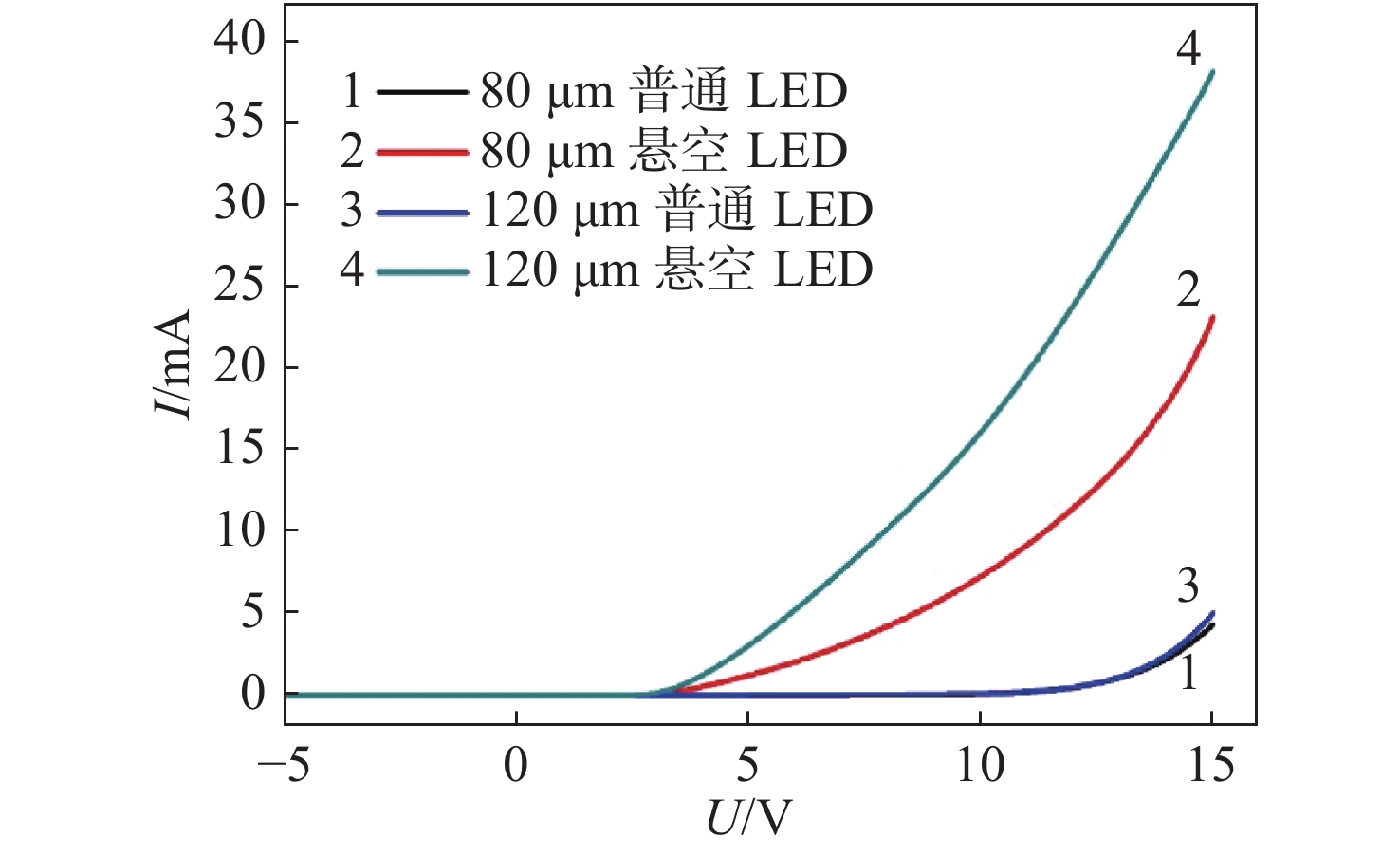
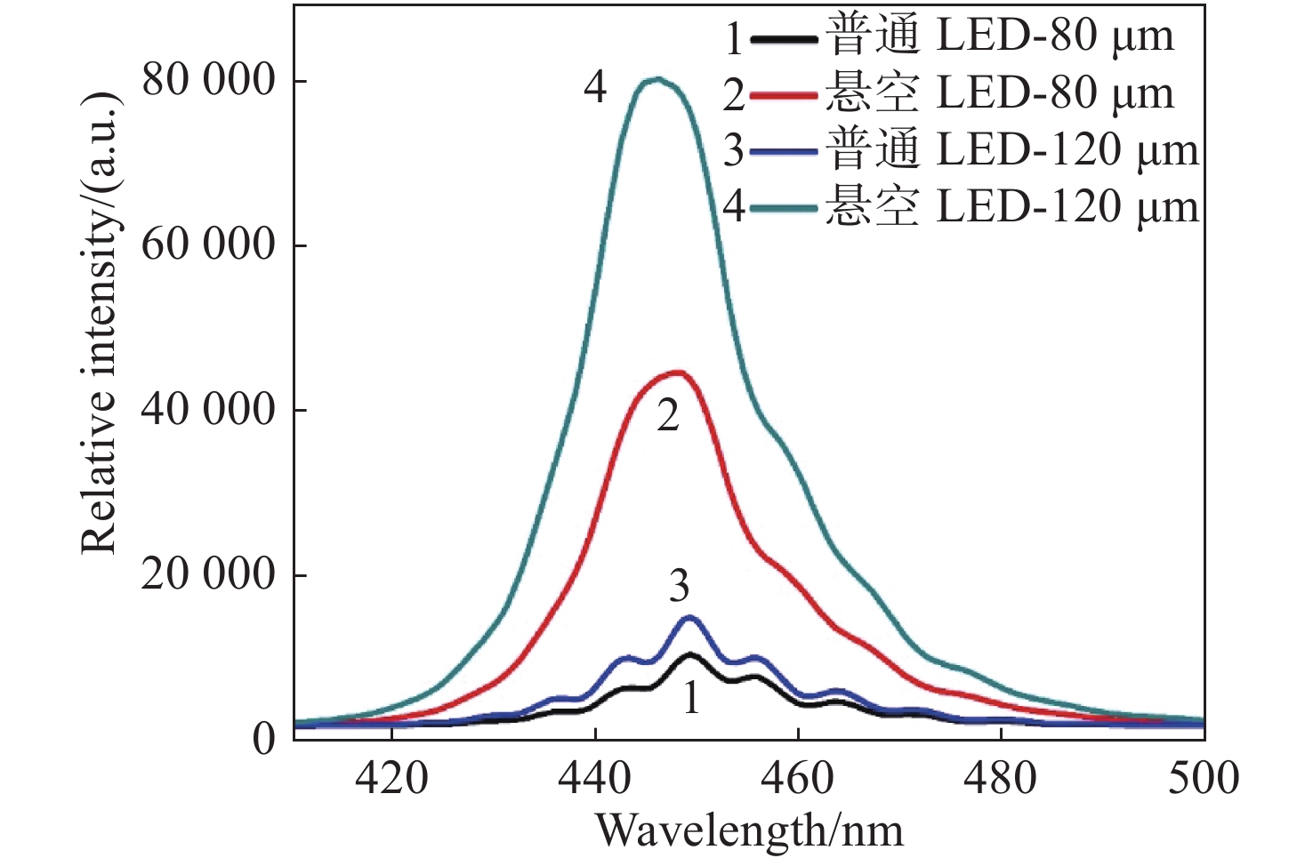
摘要: 为提升硅衬底氮化镓基LED(发光二极管)器件的光电性能和出光效率,本文提出了一种利用背后工艺实现的悬空薄膜蓝光LED器件。结合光刻工艺、深反应离子刻蚀和电感耦合等离子体反应离子刻蚀的背后工艺,制备了发光区域和大部分正负电极区域的硅衬底完全掏空,并减薄大部分氮化镓外延层的悬空薄膜LED器件。对悬空薄膜LED器件进行三维形貌表征,发现LED悬空薄膜表面平坦,变形程度小,证明背后工艺很好地解决了氮化镓外延层和硅衬底之间由于应力释放造成的薄膜变形问题。表征了LED器件的电流电压曲线和电致发光光谱等光电特性,对不同结构、不同发光区域尺寸的LED器件进行对比,发现悬空薄膜LED器件的光电性能和出光效率比普通LED器件更优越,且发光区尺寸变化对LED器件性能的影响更明显。在15 V驱动电压下,与普通LED器件相比,发光区直径为80 μm的悬空LED器件的电流从4.3 mA提升至23.9 mA。在3 mA电流的驱动下,峰值光强提升了约5倍,而发光区直径为120 μm的悬空器件与发光区直径为80 μm的悬空器件相比,出光效率提升更为明显。本研究为发展高性能悬空氮化物薄膜LED器件提供了更多可能性。Abstract: In order to improve the opto-electronic performance and light extraction efficiency of LEDs based on a GaN-on-silicon platform, we proposed an LED device based on GaN-on-silicon with an ultra-thin freestanding membrane. By combining photolithography, deep reactive ion etching and inductively-coupled plasma reactive ion etching, we prepared an LED based on a GaN-on-silicon platform with an ultra-thin freestanding membrane, removing the silicon substrate of light-emitting area and most area of the electrodes, and thinning most of the GaN epitaxial layer. We performed three-dimensional morphology characterization for the LED device and found that the surface of the LED’s membrane is flat and that the membrane’s deformation is minimal. It is proved that the back process can solve the problem of membrane deformation caused by stress release between the GaN epitaxial layer and the silicon substrate. By characterizing the current-voltage and electroluminescence spectrum of the LED and comparing the LEDs with different structures and different light-emitting area sizes, we found that the opto-electronic performance and light output efficiency of the LED with an ultra-thin freestanding membrane are better than that of the common LED, and the change in size of the light-emitting area has a significant effect on the performance of the LED. Compared with the current of common LED, the current of the LED which has an ultra-thin freestanding membrane with 80-μm diameter light-emitting area increased from 4.3 mA to 23.9 mA under 15 V driving voltage. Under 3-mA current, the peak light intensity increased by about 5 times. The light-emitting efficiency of the LED with a 120-μm diameter light-emitting area is improved more perceptibly compared with that of LED with a 80-μm diameter light-emitting area. This research provides more possibilities for the development of high-performance LED devices with an ultra-thin freestanding membrane.
-
Key words:
- gallium nitride /
- LED /
- freestanding membrane /
- back process /
- electroluminescence
-
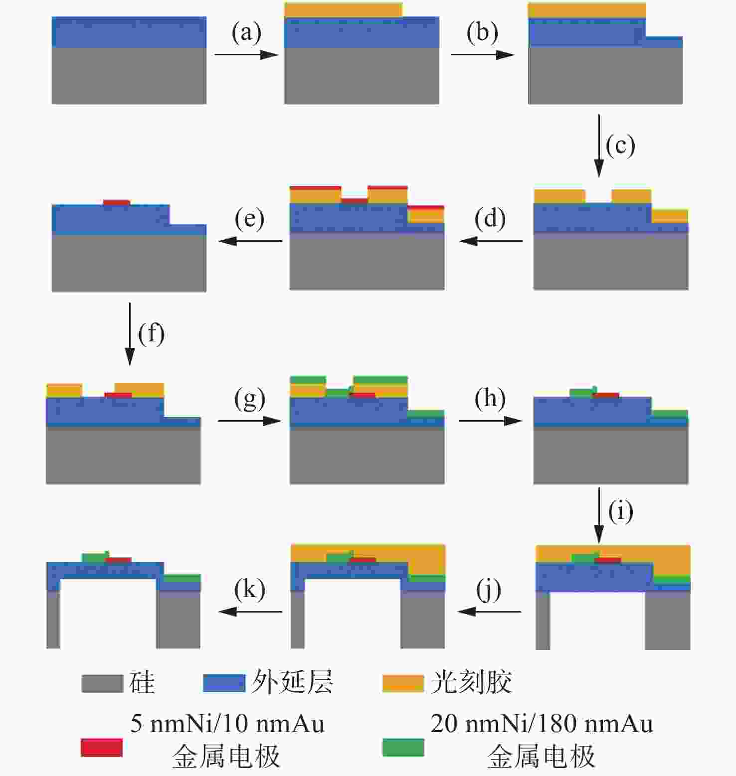
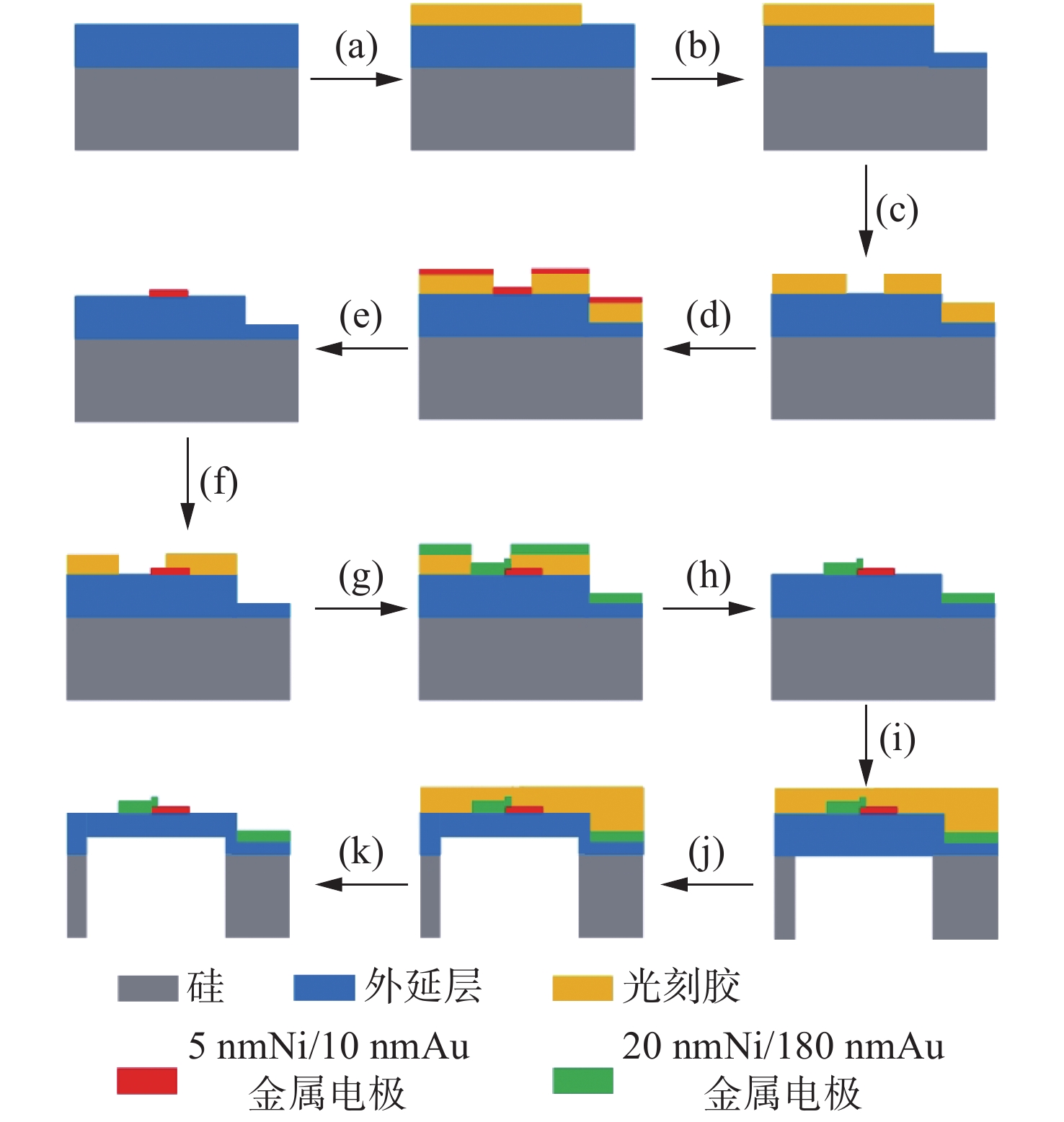
图 1 硅衬底氮化镓基悬空薄膜LED器件工艺流程图
Figure 1. Fabrication process of the GaN-based LED with an ultra-thin freestanding membrane
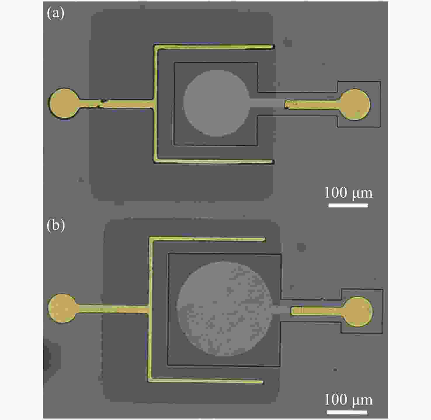
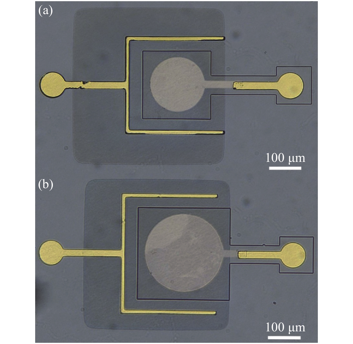
图 2 不同尺寸完全掏空硅衬底的悬空薄膜LED器件的二维形貌正视图。 (a) 发光区直径为80 μm; (b) 发光区直径为120 μm
Figure 2. Two-dimensional images of GaN-based LED device with a freestanding membrane when light emitting area’s diameter is (a) 80 μm and (b) 120 μm
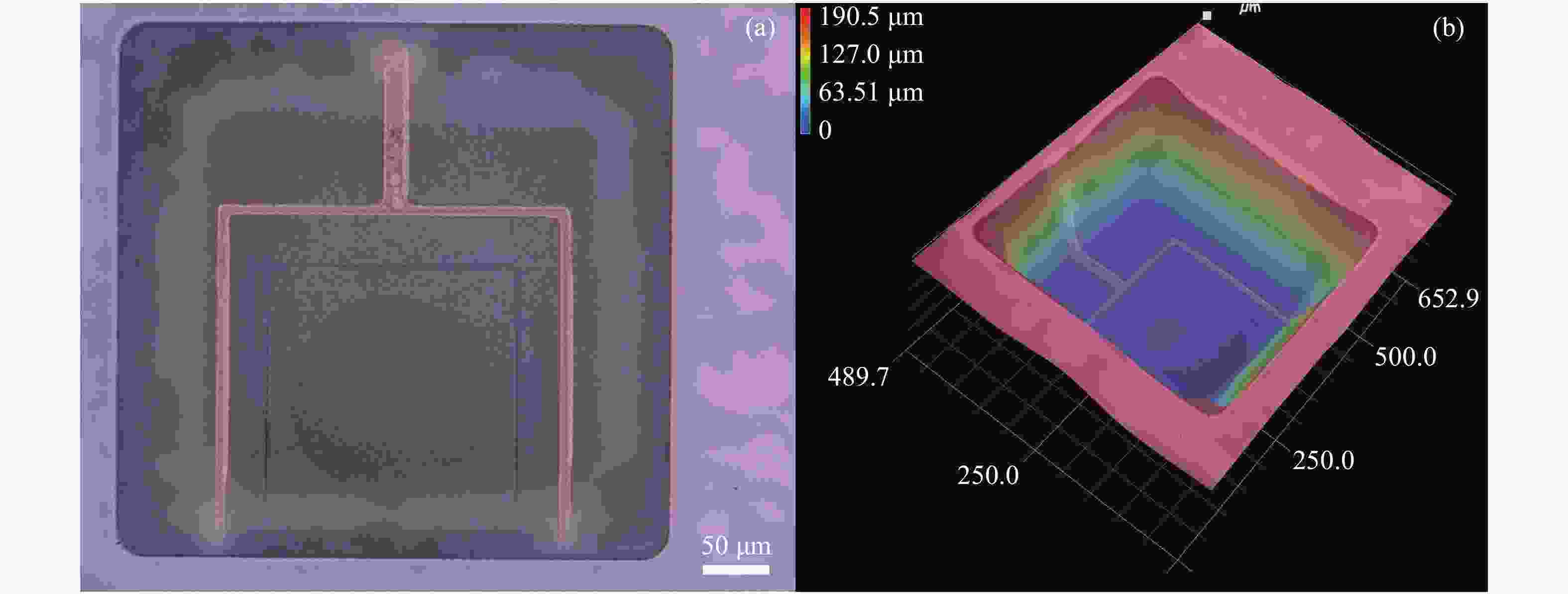
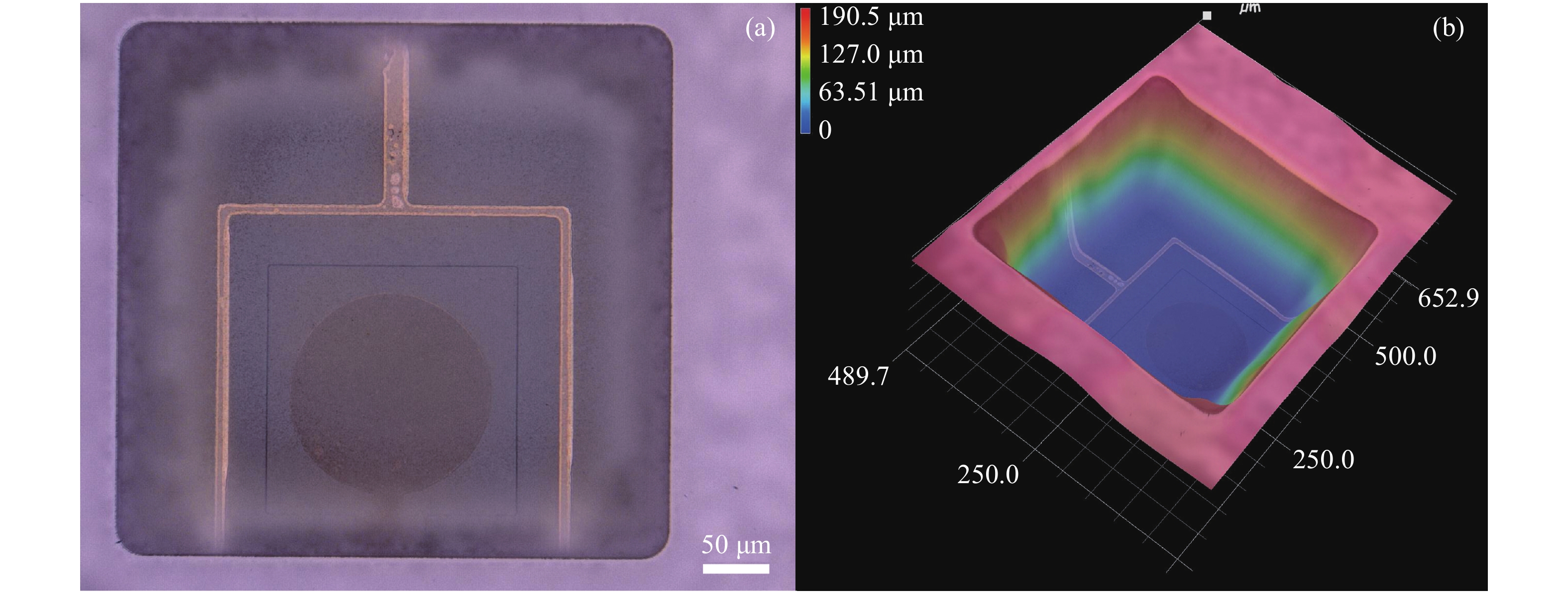
图 3 从背面观察的发光区直径为80 μm的完全掏空硅衬底的悬空薄膜LED器件的三维形貌图
Figure 3. Three-dimensional images of an LED device with a freestanding membrane with a light emitting area of 80 μm in diameter (back view)
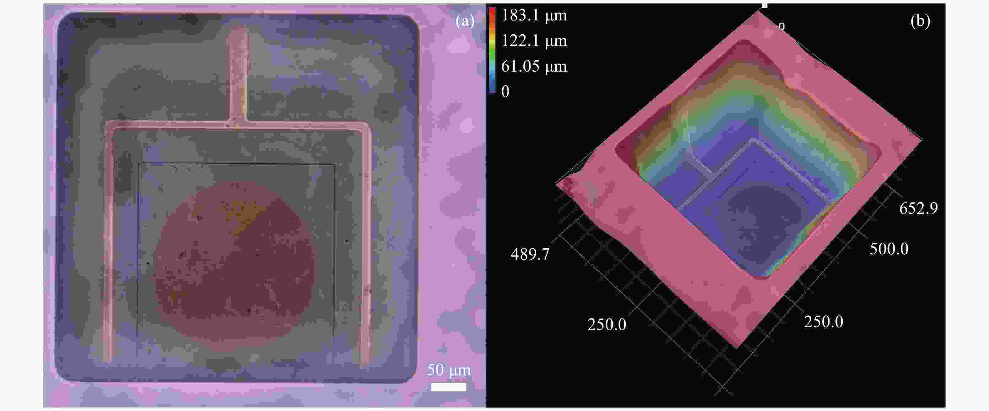
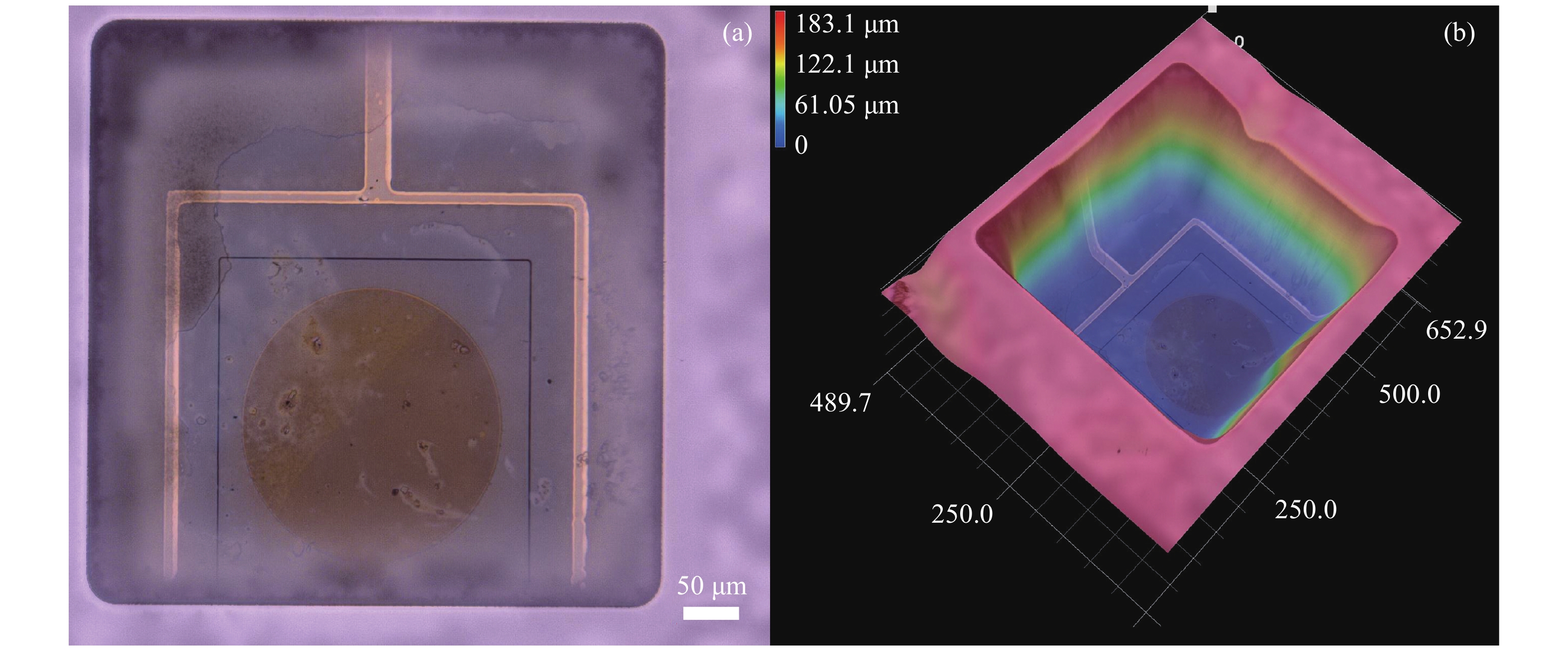
图 4 从背面观察的发光区直径为120 μm的完全掏空硅衬底的悬空薄膜LED器件的三维形貌图
Figure 4. Three-dimensional images of an LED with a freestanding membrane device with a light emitting area of 120 μm in diameter (back view)
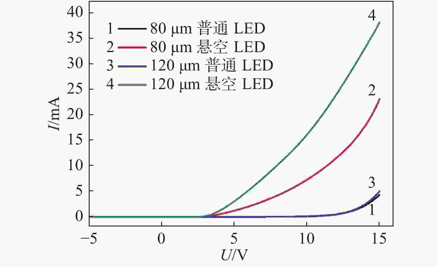
图 5 不同结构、不同尺寸LED器件的I-V(电流-电压)曲线
Figure 5. I-V (current-voltage) curves of LEDs with different structures and sizes
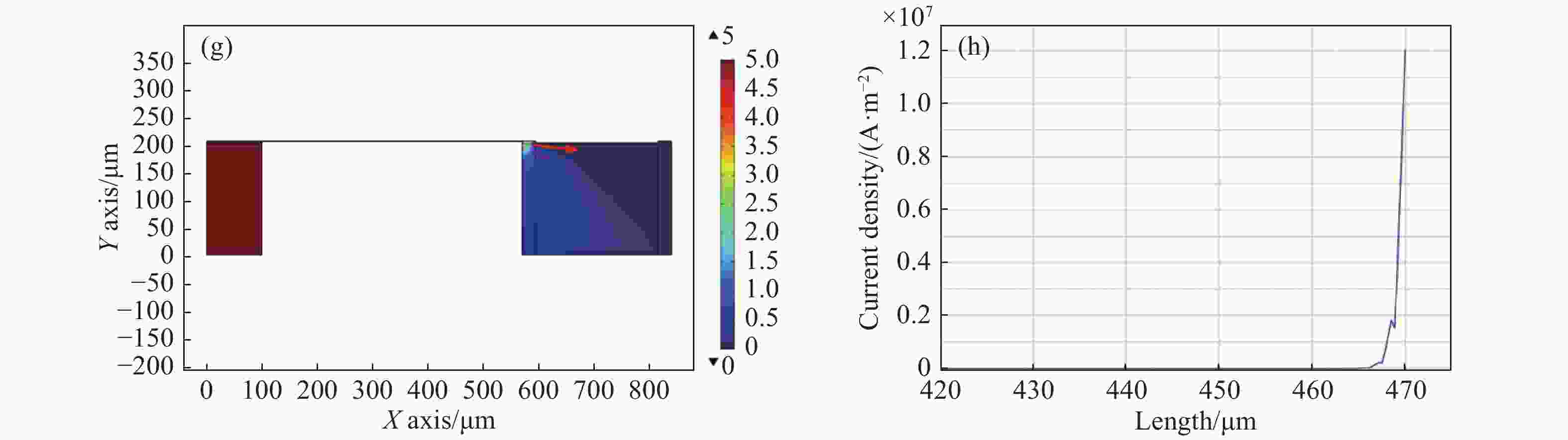
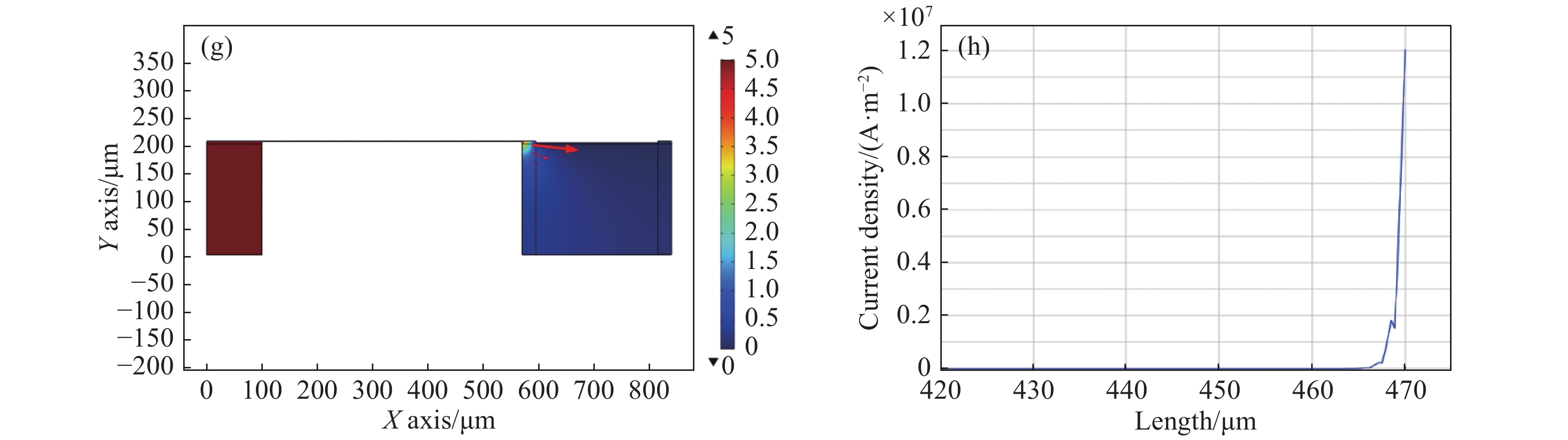
图 6 (a)普通LED器件的电势和电流密度分布及(b)普通LED器件p电极的电流密度曲线图;(c)掏空硅衬底的悬空LED器件的电势和电流密度分布;(d)掏空硅衬底的悬空LED器件p电极的电流密度曲线图;(e)掏空硅衬底并将外延层减薄至3 μm的悬空LED器件的电势和电流密度分布;(f)掏空硅衬底并将外延层减薄至3 μm的悬空LED器件p电极的电流密度曲线图;(g)掏空硅衬底并将外延层减薄至1 μm的悬空LED器件的电势和电流密度分布;(h)掏空硅衬底并将外延层减薄至1 μm的悬空LED器件p电极的电流密度曲线图。
Figure 6. (a) Distribution of the potential and current density and (b) p electrode current density curve of the common LED; (c) distribution of the potential and current density and (d) p electrode current density curve of the LED with a membrane but without a silicon substrate; (e) distribution of potential and current density and (f) p electrode current density curve of the LED with a membrane and a GaN epitaxial layer thinned to 3 μm; (g) distribution of potential and current density and (h) p electrode current density curve of the LED with a membrane and a GaN epitaxial layer thinned to 1 μm
图 7 发光区直径均为120 μm,结构不同的LED器件在刚好到达开启电压的情况下的发光情况。 (a) 普通LED; (b) 悬空薄膜LED
Figure 7. The light-emitting images of the LED with different structures and with light-emitting area’s diameter of 120 μm when its voltage is turned on. (a) Common LED; (b) LED with a freestanding membrane
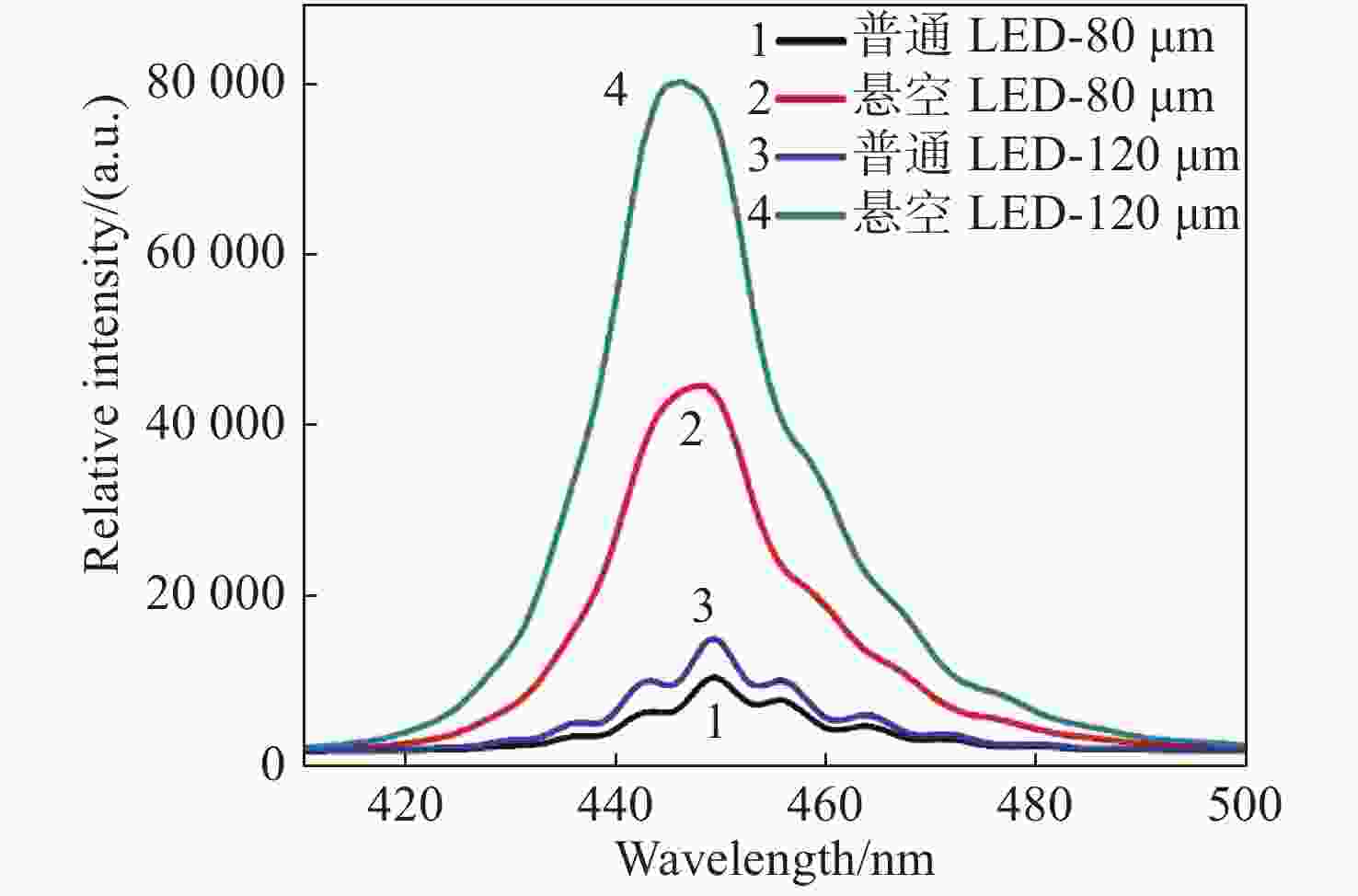
图 8 不同尺寸和不同结构的LED器件的电致发光光谱
Figure 8. Electroluminescence spectra of the LEDs with different sizes and structures
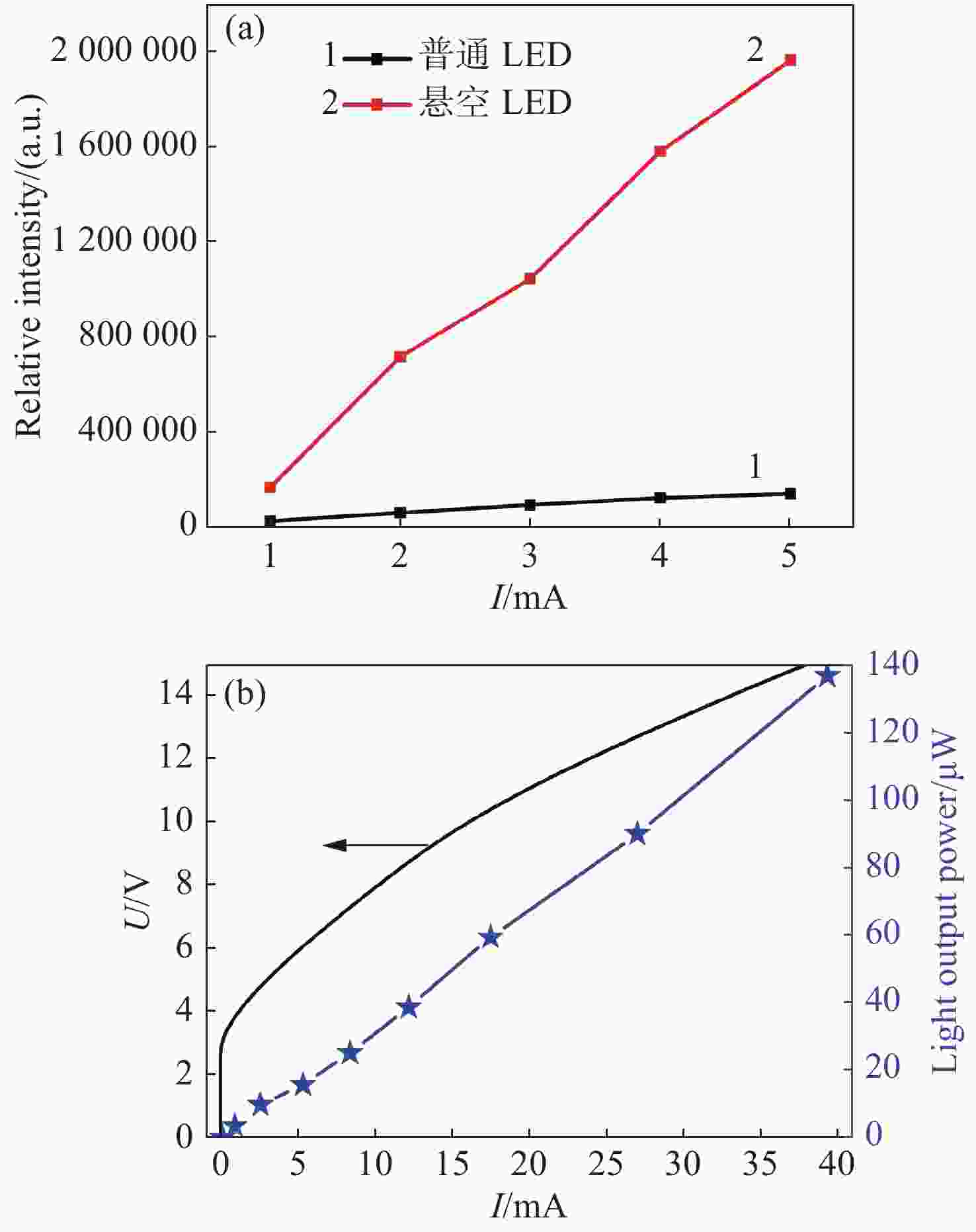
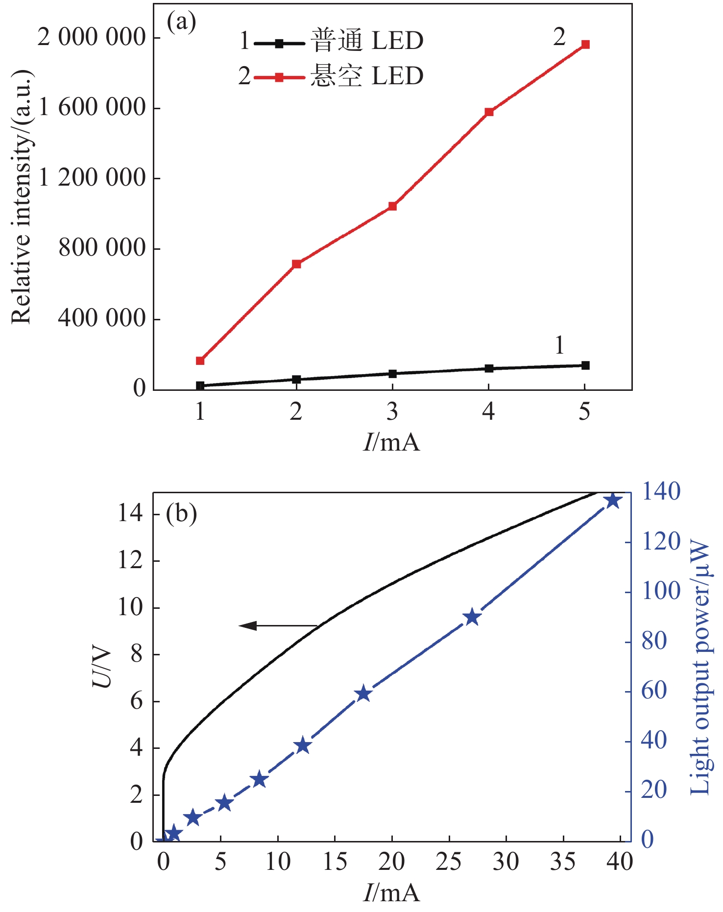
图 9 (a) 发光区直径为120 μm的结构不同的LED器件电致发光情况下总光强对比; (b) 发光区直径为120 μm的悬空薄膜LED器件的光功率-电压-电流曲线
Figure 9. (a) Comparison of the electroluminescence total light intensities of the LED with different structures when light emitting area’s diameter is 120 μm; (b) L-V-I (light output power-voltage-current) curves of the LED with a 120 μm-diameter light emitting area and with a freestanding membrane
-
[1] 张雨茜, 陆志成, 张伟, 等. 硅基纳米柱GaN-LED的制备与光谱特性分析[J]. 光谱学与光谱分析,2019,39(8):2450-2453.ZHANG Y X, LU ZH CH, ZHANG W, et al. Study of the fabrication and spectral analysis of silicon-based nanocolumn GaN-LED[J]. Spectroscopy and Spectral Analysis, 2019, 39(8): 2450-2453. (in Chinese) [2] 江孝伟, 赵建伟, 武华. 高光提取效率倒装发光二极管的设计与优化[J]. 激光与光电子学进展,2018,55(9):092302.JIANG X W, ZHAO J W, WU H. Design and optimization of flip-chip light-emitting diode with high light extraction efficiency[J]. Laser &Optoelectronics Progress, 2018, 55(9): 092302. (in Chinese) [3] 洪国彬, 杨钧杰, 卢廷昌. 蓝紫光氮化镓光子晶体面射型激光器[J]. 中国光学,2014,7(4):559-571.HONG G B, YANG J J, LU T CH. Blue-violet GaN-based photonic crystal surface emitting lasers[J]. Chinese Optics, 2014, 7(4): 559-571. (in Chinese) [4] ALHASSAN A I, YOUNG E C, ALYAMANI A Y, et al. Reduced-droop green III–nitride light-emitting diodes utilizing GaN tunnel junction[J]. Applied Physics Express, 2018, 11(4): 042101. doi: 10.7567/APEX.11.042101 [5] WONG M S, NAKAMURA S, DENBAARS S P. Review-progress in high performance III-Nitride micro-light-emitting diodes[J]. ECS Journal of Solid State Science and Technology, 2020, 9(1): 015012. doi: 10.1149/2.0302001JSS [6] WU T ZH, SHER C W, LIN Y, et al. Mini-LED and micro-LED: promising candidates for the next generation display technology[J]. Applied Sciences, 2018, 8(9): 1557. doi: 10.3390/app8091557 [7] ZHANG X, LI P A, ZOU X B, et al. Active matrix monolithic LED micro-display using GaN-on-Si epilayers[J]. IEEE Photonics Technology Letters, 2019, 31(11): 865-868. doi: 10.1109/LPT.2019.2910729 [8] KOESTER R, SAGER D, QUITSCH W A, et al. High-speed GaN/GaInN nanowire array light-emitting diode on silicon(111)[J]. Nano Letters, 2015, 15(4): 2318-2323. doi: 10.1021/nl504447j [9] HORNG R H, WU B R, TIEN C H, et al. Performance of GaN-based light-emitting diodes fabricated using GaN epilayers grown on silicon substrates[J]. Optics Express, 2014, 22(S1): A179-A187. doi: 10.1364/OE.22.00A179 [10] MONAVARIAN M, RASHIDI A, ARAGON A A, et al. Impact of crystal orientation on the modulation bandwidth of InGaN/GaN light-emitting diodes[J]. Applied Physics Letters, 2018, 112(4): 041104. doi: 10.1063/1.5019730 [11] YANG J, ZHAO D G, JIANG D S, et al. Emission efficiency enhanced by introduction of the homogeneous localization states in InGaN/GaN multiple quantum well LEDs[J]. Journal of Alloys and Compounds, 2016, 681: 522-526. doi: 10.1016/j.jallcom.2016.04.259 [12] ISHIKAWA H, ASANO K, ZHANG B, et al. Improved characteristics of GaN-based light-emitting diodes by distributed Bragg reflector grown on Si[J]. Physica Status Solidi (A) , 2004, 201(12): 2653-2657. [13] ISHIKAWA H, JIMBO T, EGAWA T. GaInN light emitting diodes with AlInN/GaN distributed Bragg reflector on Si[J]. Physica Status Solidi C, 2008, 5(6): 2086-2088. doi: 10.1002/pssc.200778441 [14] ZHANG B J, EGAWA T, ISHIKAWA H, et al. Thin-film InGaN multiple-quantum-well light-emitting diodes transferred from Si (111) substrate onto copper carrier by selective lift-off[J]. Applied Physics Letters, 2005, 86(7): 071113. doi: 10.1063/1.1863412 [15] DENG D M, YU N S, WANG Y, et al. InGaN-based light-emitting diodes grown and fabricated on nanopatterned Si substrates[J]. Applied Physics Letters, 2010, 96(20): 201106. doi: 10.1063/1.3427438 [16] CHIU C H, LIN C C, DENG D M, et al. Optical and electrical properties of GaN-Based light emitting diodes grown on micro- and nano-scale patterned Si substrate[J]. IEEE Journal of Quantum Electronics, 2011, 47(7): 899-906. doi: 10.1109/JQE.2011.2114640 [17] WAKUI M, SAMESHIMA H, HU F R, et al. Fabrication of GaN light emitting diode membrane on Si substrate for MEMS applications[J]. Microsystem Technologies, 2011, 17(1): 109-114. doi: 10.1007/s00542-010-1151-4 [18] NAKAZATO H, KAWAGUCHI H, IWABUCHI A, et al. Micro fluorescent analysis system integrating GaN-light-emitting-diode on a silicon platform[J]. Lab on a Chip, 2012, 12(18): 3419-3425. doi: 10.1039/c2lc40178a [19] LI X, SHI ZH, ZHU G Y, et al. High efficiency membrane light emitting diode fabricated by back wafer thinning technique[J]. Applied Physics Letters, 2014, 105(3): 031109. doi: 10.1063/1.4890859 [20] 李欣, 沙源清, 蒋成伟, 等. 超薄氮化镓基LED悬空薄膜的制备及表征[J]. 中国光学,2020,13(4):873-883. doi: 10.37188/CO.2019-0192LI X, SHA Y Q, JIANG CH W, et al. Fabrication and characterization of ultra-thin GaN-based LED freestanding membrane[J]. Chinese Optics, 2020, 13(4): 873-883. (in Chinese) doi: 10.37188/CO.2019-0192 [21] KANG B S, KIM S, KIM J, et al. Effect of external strain on the conductivity of AlGaN/GaN high-electron-mobility transistors[J]. Applied Physics Letters, 2003, 83(23): 4845-4847. doi: 10.1063/1.1631054 -

 下载:
下载:


计量
- 文章访问数: 3165
- HTML全文浏览量: 777
- PDF下载量: 196
- 被引次数: 0
