


Progress on defect and related carrier dynamics in two-dimensional transition metal chalcogenides
-
摘要: 原子级厚度的单层或者少层二维过渡金属硫族化合物因其独特的物理特性而被寄希望成为下一代光电子器件的重要组成部分。然而,二维材料的缺陷在很大程度上影响着材料的性质。一方面,缺陷的存在降低了材料的荧光量子效率、载流子迁移率等重要参数,影响了器件的性能。另一方面,合理地调控和利用缺陷催生了单光子源等新的应用,因此,表征、理解、处理和调控二维材料中的缺陷至关重要。本文综述了二维过渡金属硫族化合物中的缺陷以及缺陷相关的载流子动力学研究进展,旨在梳理二维材料中的缺陷及其超快动力学与材料性能之间的关系,为二维过渡金属硫族化合物材料特性和高性能光电子器件的相关研究提供支持。Abstract: Because of their unique physical properties, the monolayer and few-layer two-dimensional transition metal chalcogenides with atomic-level thickness are expected to play an important role in the next generation of optoelectronic devices. However, defects in two-dimensional materials affect their properties to a great extent. On one hand, defects reduce the fluorescence quantum efficiency, carrier mobility and other important device parameters. On the other hand, the control and utilization of defects have given birth to new techniques such as using single-photon sources. Therefore, it is very important to characterize, understand, handle and control the defects in two-dimensional materials. In this review, the research progress on defects and its related carrier dynamics in two-dimensional transition metal chalcogenides is summarized. This paper aims to sort out the great influence of defects and their related ultrafast dynamics on material performance in two-dimensional transition metal chalcogenides, and to support studies on fundamental physical properties and high-performance optoelectronic devices.
-
Key words:
- two-dimensional materials /
- transition metal chalcogenides /
- defects /
- carrier dynamics
-
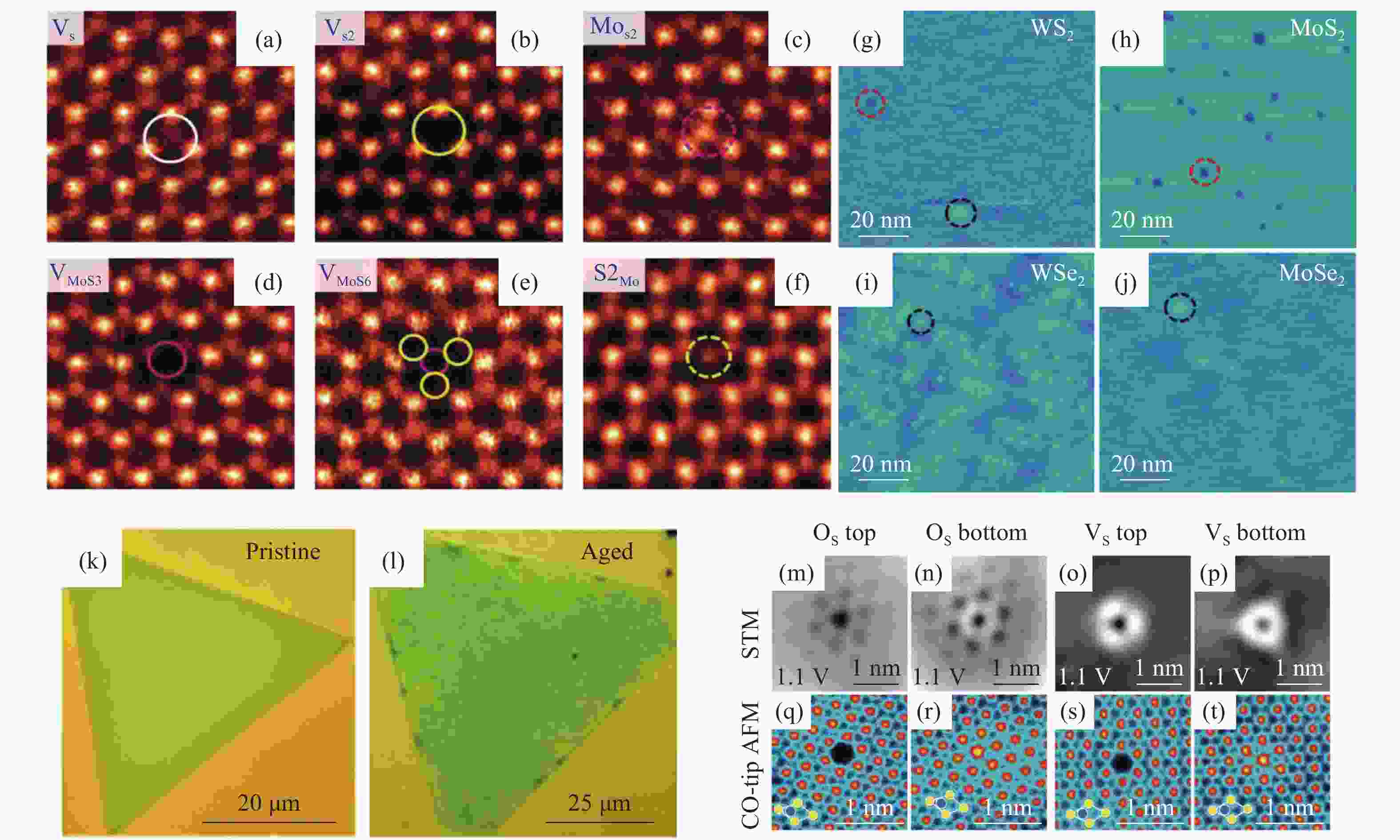
图 1 二维TMDCs中点缺陷的高分辨表征。 (a−f) STEM-ADF对MoS2中6种点缺陷的表征[85];(g−j)4种常见的TMDCs材料中缺陷的STM表征,深蓝色的点代表原子缺失或存在受体杂质,亮黄色的点代表存在给体杂质[86];(k)新制备的MoS2与(l)在大气中放置8个月后的光学显微镜照片的对比[90];(m−t)超高分辨STM和非接触式AFM对WS2中点缺陷的表征[88]
Figure 1. High resolution characterization of point defects in 2D TMDCs. (a−f) STEM-ADF characterization of six kinds of point defect in MoS2[85]; (g−j) STM characterization of defects in four common TMDCs materials, where dark blue points represent atom defects or receptor impurities, bright yellow points represent donor impurities[86]; comparison of optical microscope pictures between (k) fresh MoS2 and (l) fresh MoS2 after 8 months of atmospheric exposure[90]; (m−t) ultra-high resolution STM and non-contact AFM characterization of point defects in WS2[88]
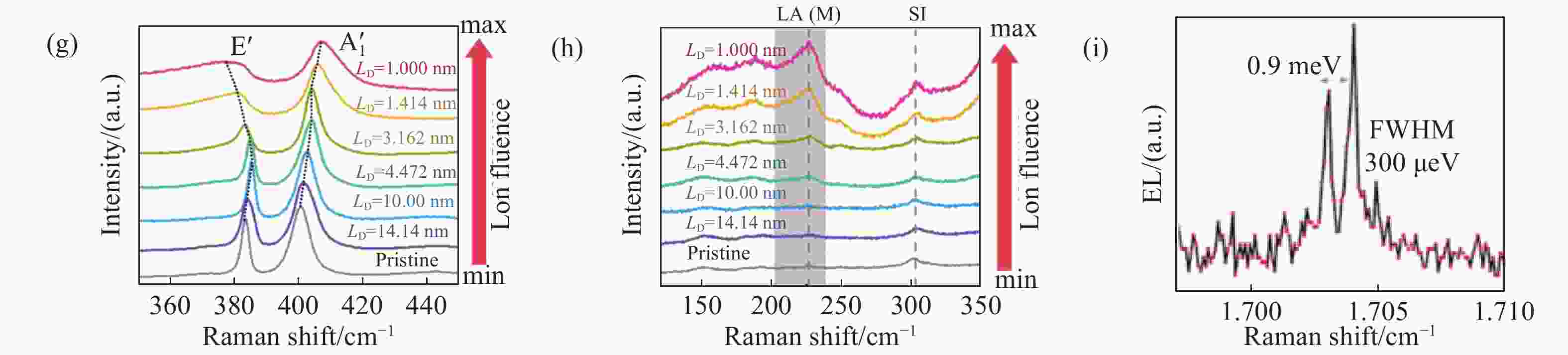
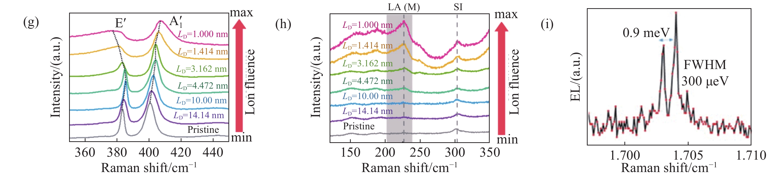
图 2 缺陷的稳态光谱学研究。 (a)电子束、等离子体、紫外光可以在TMDCs中产生缺陷;(b)单层WSe2随氩等离子体处理时间变化的荧光光谱[103];(c)使用氩等离子和电子束处理单层WSe2后的荧光光谱[103];(d)单层MoS2随电压(上图)、泵浦功率(中图)、温度(下图)改变的荧光光谱[110];(e)缺陷捕获激子的模型(上图),束缚态激子/激子发光占比(左侧坐标轴)与带电激子/激子发光占比(右侧坐标轴)随栅压的变化(下图)[110];(f)DFT计算得到的存在缺陷的WS2的能带结构(左图)和跃迁偶极矩(右图)[115];(g)(h)随着离子束处理强度增加,单层MoS2拉曼光谱的变化[120];(i)单层WSe2中缺陷的EL光谱[130]
Figure 2. Steady state spectroscopic studies of defects. (a) The defects can be produced in TMDCs by electron beam, plasma and ultraviolet irradiation; (b) fluorescence spectrum of monolayer WSe2 as it changes with varying argon plasma treatment[103]; (c) fluorescence spectrum of monolayer WSe2 after argon plasma and electron beam treatment[103]; (d) fluorescence spectrum of monolayer MoS2 as it changes with voltage (above), pump power (center) and temperature (below)[110]; (e) defect capture exciton model (above), the bound exciton/exciton PL intensity ratio (left axis) and the trion/exciton PL intensity ratio (right axis) vary with the gate voltage (below)[110]; (f) band structure (left) and the transition dipole moment (right) of defected monolayer WS2 calculated by DFT[115]; (g)(h) Raman spectrum of monolayer MoS2 with respect to ion beam treatment intensity[120]; (i) electroluminescence spectra of defects in monolayer WSe2[130]
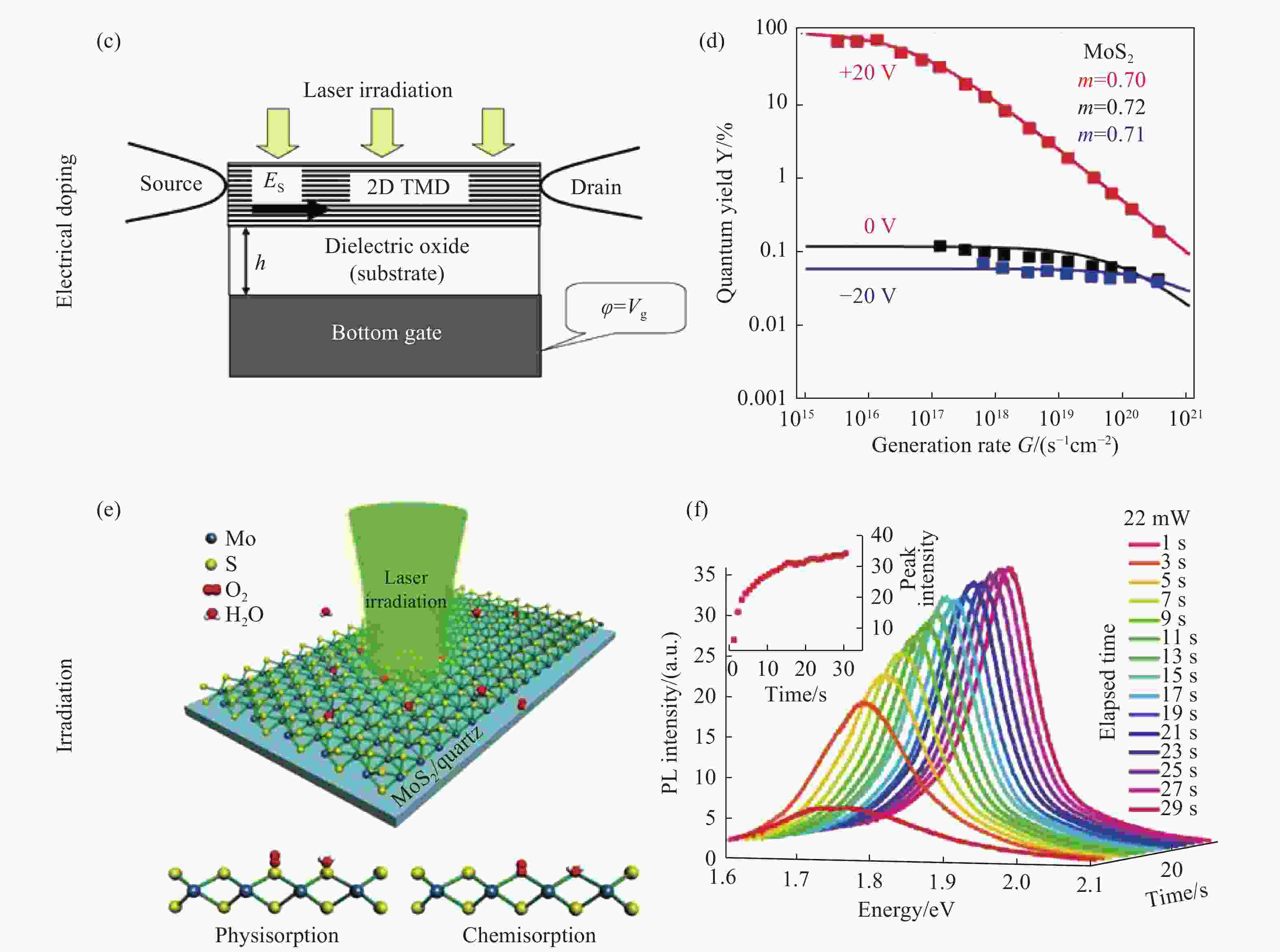
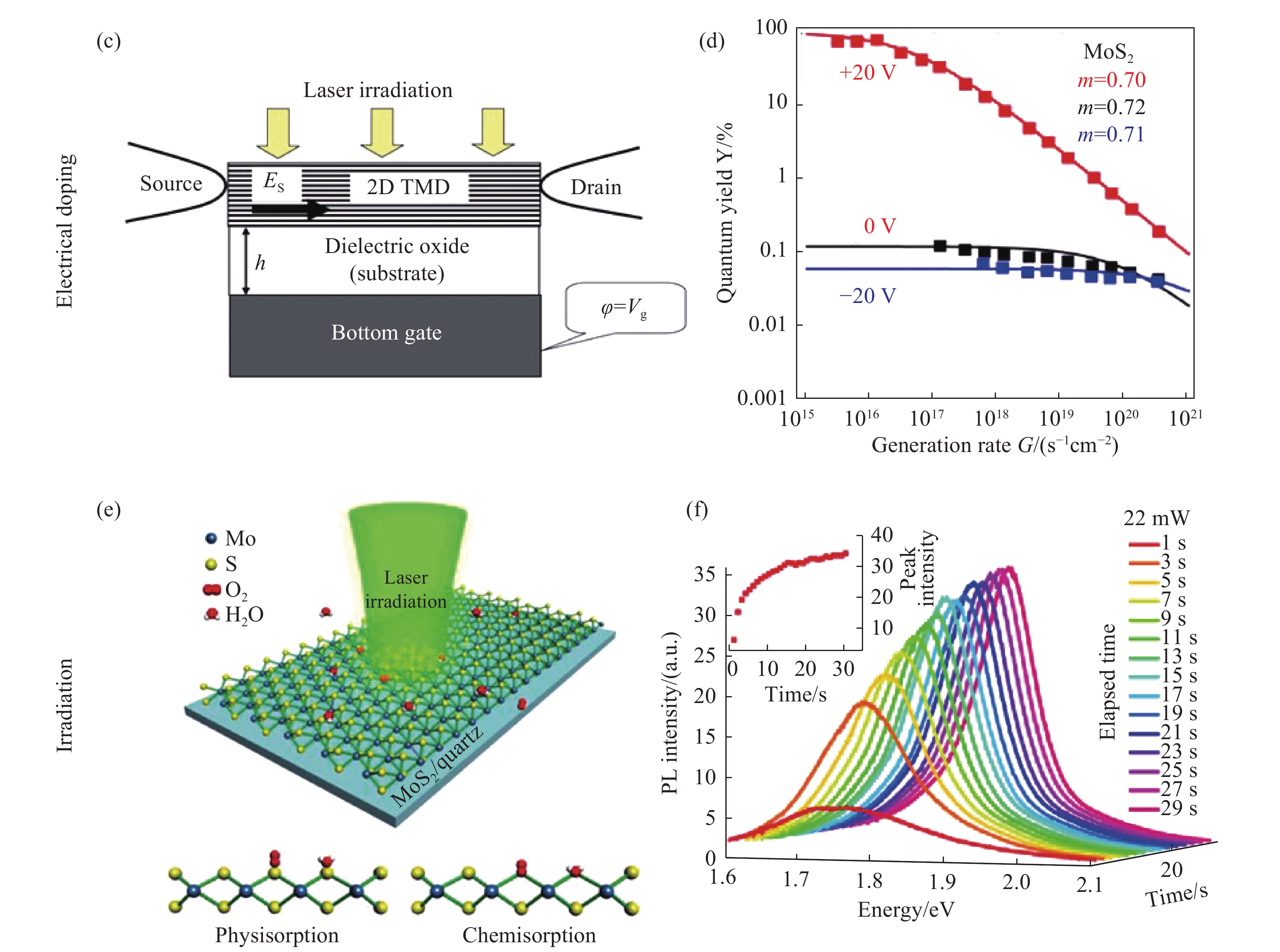
图 3 缺陷态发光的抑制。 (a)使用“超级酸”处理单层MoS2并使用含氟聚合物进行封装[134];(b) 使用“超级酸”处理单层MoS2前后的荧光光谱[134];(c)使用静电掺杂调节单层MoS2的PLQY的器件结构和原理图[142];(d)改变栅压和泵浦功率时MoS2的PLQY的变化[142];(e)使用激光照射处理MoS2的示意图(上图)和发生的氧气物理吸附与化学吸附(下图)[146];(f)对久置的MoS2进行激光照射时荧光光谱随照射时间的变化[147]
Figure 3. Suppression of defect state luminescence. (a) Treating the monolayer MoS2 with "super acid" and encapsulating it with CYTOP[134]; (b) fluorescence spectrum before and after treatment[134]; (c) device structure and schematic diagram of PLQY tuning of the monolayer MoS2 through electrostatic doping[142]; (d) PLQY of monolayer MoS2 changes with the gate voltage and pump power[142]; (e) schematic diagram of the MoS2 treated by laser irradiation (above) and occurred oxygen physisorption and chemisorption (below)[146]; (f) fluorescence spectrum of aged MoS2 changing with time irradiated by laser[147]
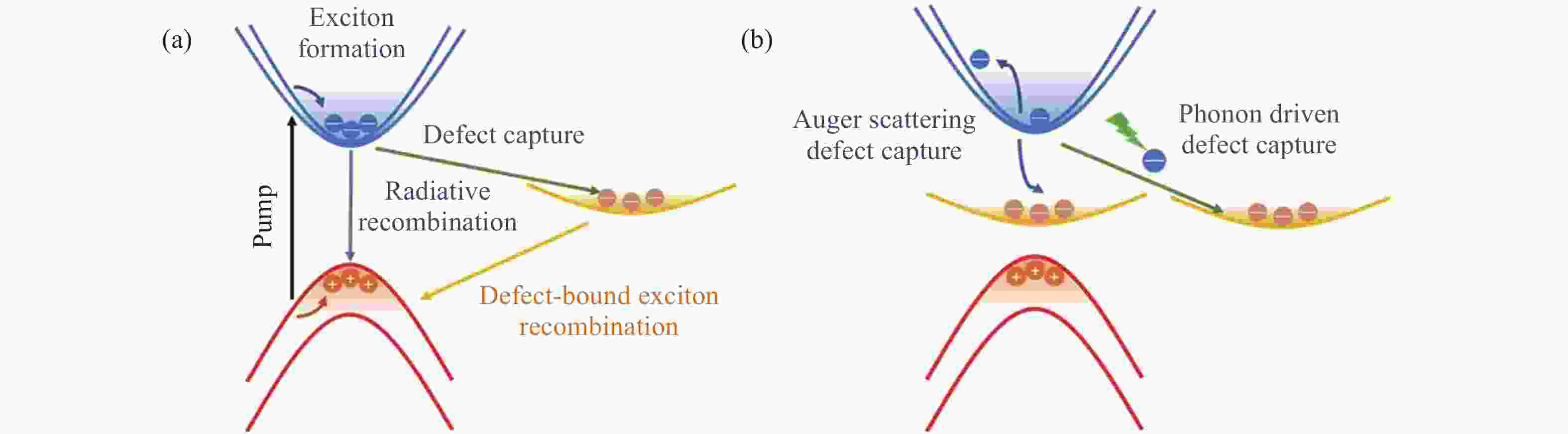
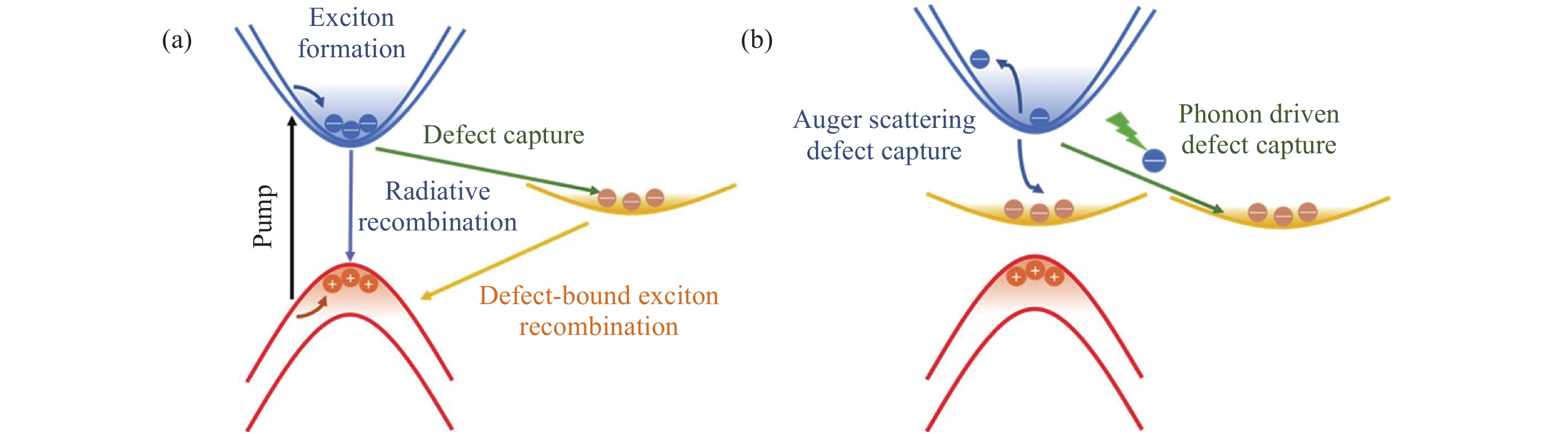
图 4 (a) TMDCs中的载流子动力学和(b)缺陷捕获过程
Figure 4. (a) Carrier dynamics and (b) defect capture process in TMDCs
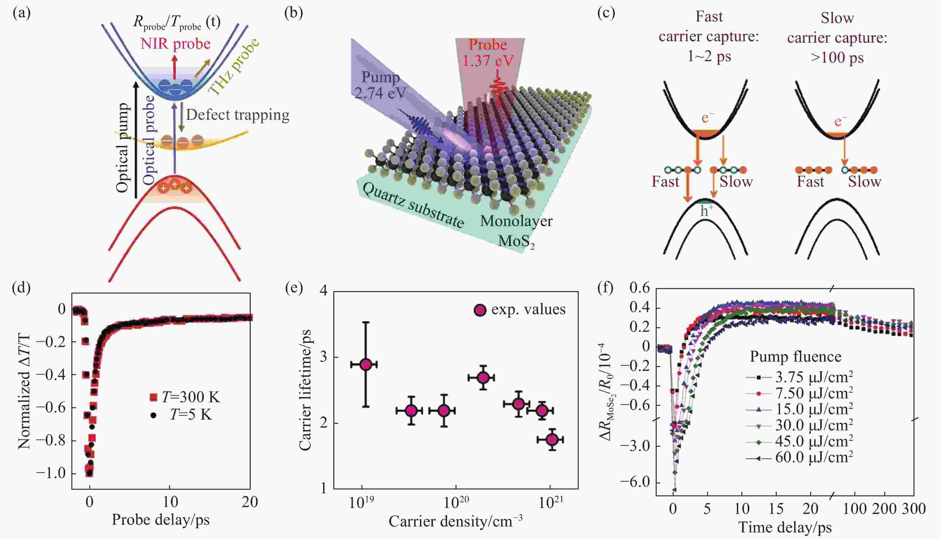
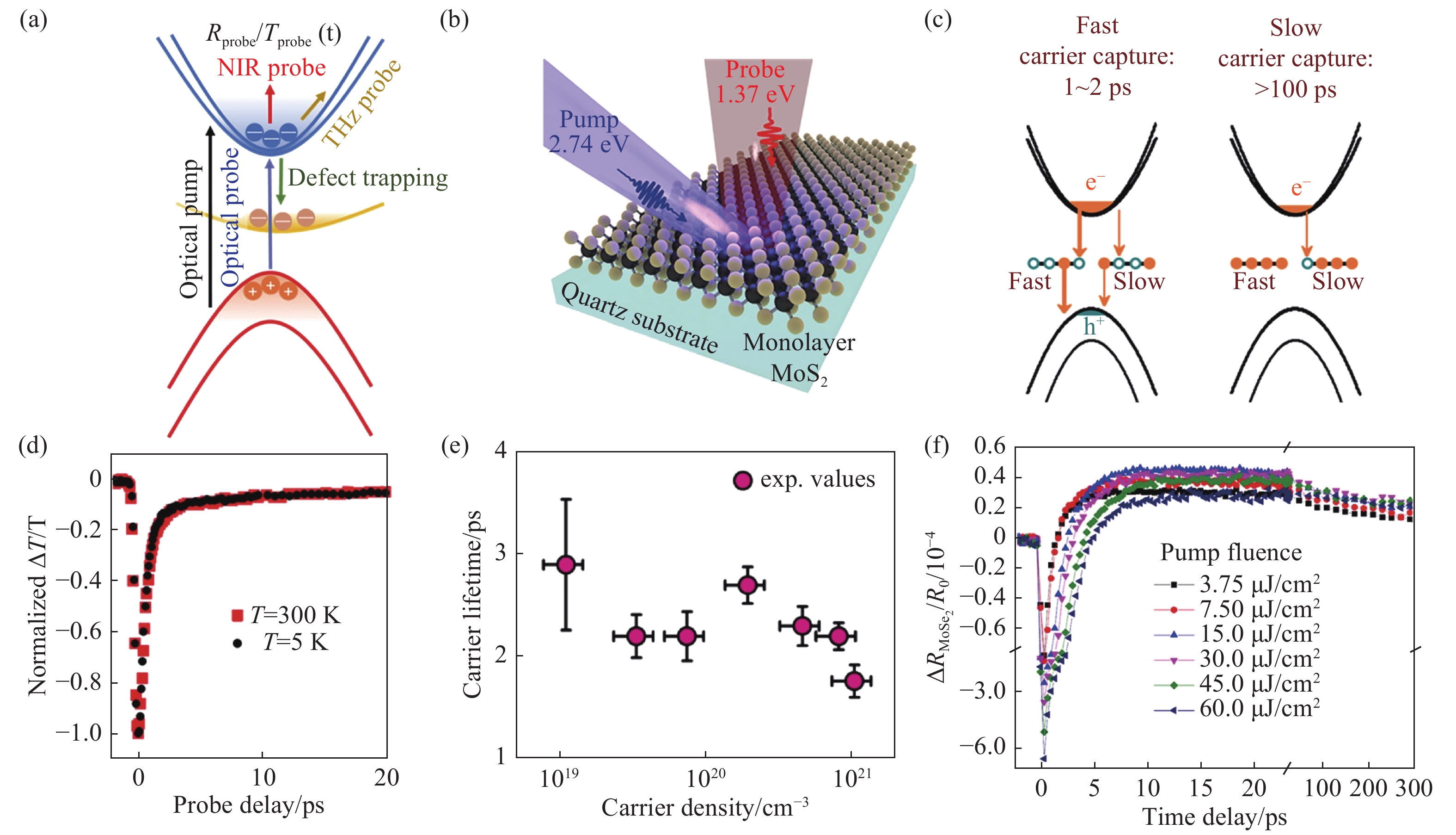
图 5 基于瞬态吸收光谱对TMDCs缺陷相关的载流子动力学的研究 。(a)使用泵浦-探测方法对缺陷态进行探测的示意图;(b)泵浦光和探测光打在样品的相同位置,两束光通过位移台改变到达的时间差[62];(c)缺陷捕获载流子的快通道(左图)和慢通道(右图)的示意图[62];(d)不同温度下单层MoS2对探测光的透射率随时间的变化[62];(e)不同功率下少层MoTe2载流子寿命的变化[63];(f)不同功率下单层MoSe2对探测光的反射率随时间的变化[159]
Figure 5. Studies on defect related carrier dynamics of TMDCs based on transient absorption spectroscopy. (a) Schematic diagram of detecting the defect state by using the pump-probe method; (b) pump light and the probe light illuminate the same position of the sample. The time difference of two light beams changing through optical path difference[62]; (c) schematic diagram of the fast channel (left) and the slow channel (right) of the defect trapping process[62]; (d) the transmittance of the monolayer MoS2 to the probe light varying with time under different temperatures[62]; (e) change of carrier lifetime of MoTe2 at different pump powers[63]; (f) change in reflectivity of the monolayer MoSe2 with respect to time at different pump powers[159]
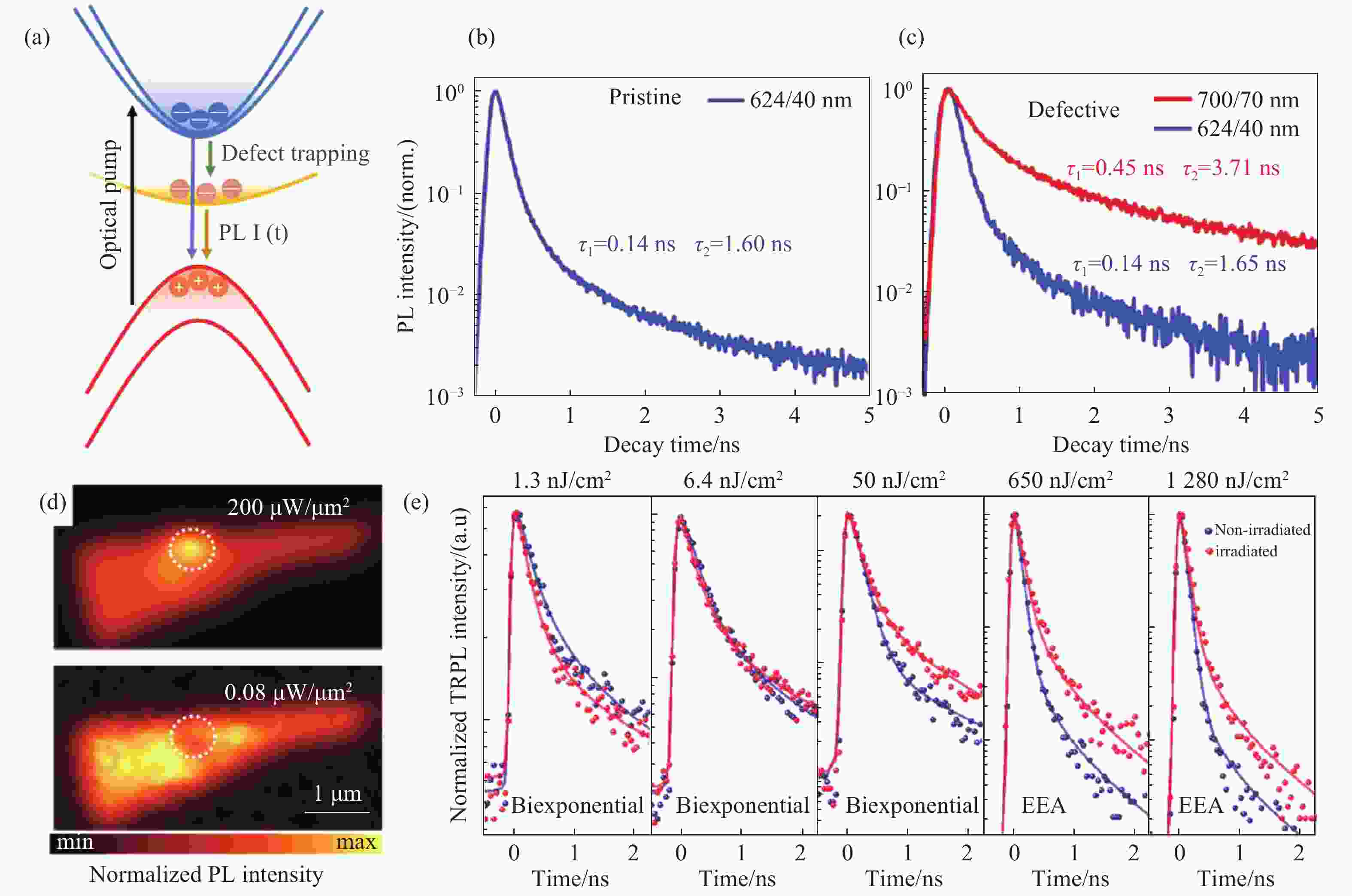
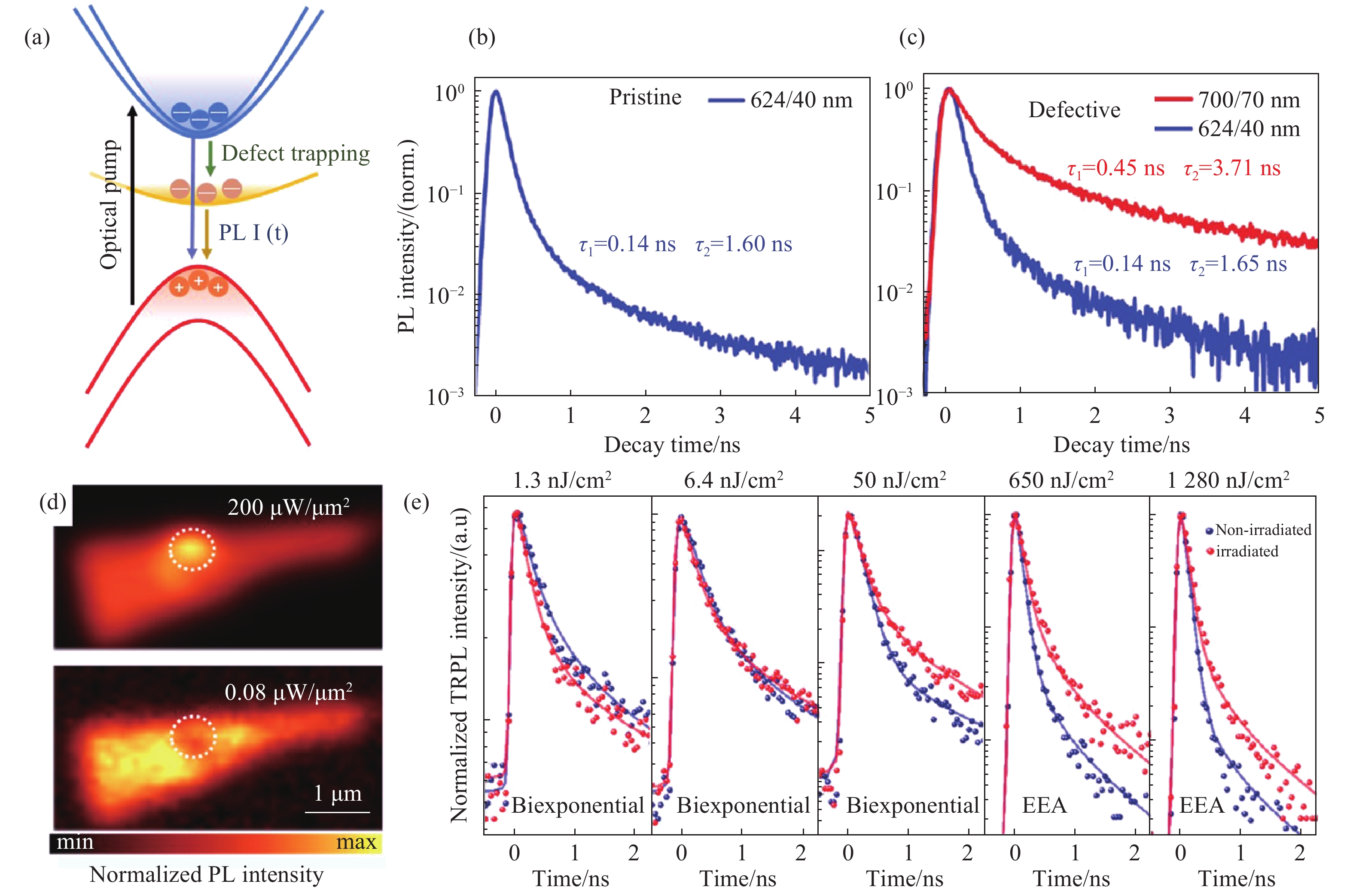
图 6 基于时间分辨荧光光谱对TMDCs缺陷相关的载流子动力学的研究。 (a)时间分辨荧光对缺陷态进行探测的原理图;(b)本征WS2自由激子的荧光衰减曲线[157];(c)使用氩离子束轰击产生缺陷后WS2的自由激子(蓝线)和束缚态激子(红线)的荧光衰减曲线[157];(d)使用激光对单层WS2进行预处理后(圆圈区域),高功率(上图)和低功率(下图)的荧光强度对比,两张图中的强度都用各图的最高强度进行了归一化[148];(e)单层WS2的荧光在不同激发功率下的荧光衰减曲线,蓝线为预先使用激光照射,红色为未提前处理[148]
Figure 6. Studies of defect-related carrier dynamics in TMDCs using TRPL spectroscopy. (a) Schematic diagram of TRPL to detect the defect state; (b) PL decay curve of free exciton energy in pristine monolayer WS2[157]; (c) PL decay curves of the free exciton (blue line) and the bound exciton (red line) energy in the defective monolayer WS2 after being irradiated by an argon ion beam[157]; (d) comparison of the PL intensities of the monolayer WS2 pretreated by laser (circle area) at a high pump power (above) and a low pump power (below)[148]; (e) PL decay curve of the monolayer WS2 under different excitation powers. The blue line represents the sample before being irradiated by laser, and the red line presents that not having been pretreated[148]

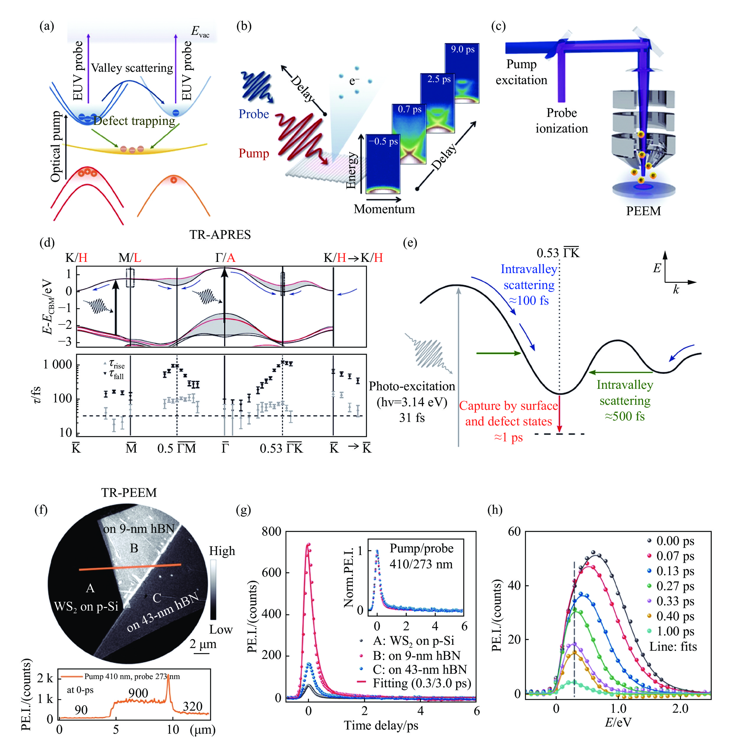
图 7 基于时间分辨ARPES和PEEM对TMDCs缺陷相关的载流子动力学的研究。 (a)时间分辨ARPES和PEEM对缺陷态进行探测的原理图;(b)时间分辨ARPES对动量空间进行探测的原理图[175];(c)时间分辨PEEM对样品表面光电子成像的原理图[64];(d)理论计算得到的MoS2的动量空间与探测的动量区域(灰色阴影)(上图),时间分辨APRES实验测得的动量空间不同位置光电子发射信号的上升和下降时间[161];(e)脉冲光激发后MoS2动量空间谷间散射和缺陷捕获的示意图[161];(f)泵浦探测零时刻PEEM对单层WS2的实空间成像(上图),三种覆盖单层WS2的不同区域的光电子发射信号强度(下图)[64];(g)三种区域光电子发射信号强度随时间的变化[64];(h)光电子发射信号强度的能量分布随泵浦探测时间差的变化[64]
Figure 7. Study of defect related carrier dynamics in TMDCs based on time-resolved ARPES and PEEM. (a) Schematic diagram of time-resolved ARPES and PEEM for detecting the defect state; (b) schematic diagram of time-resolved ARPES for detecting momentum space[175]; (c) schematic diagram of time-resolved PEEM for photoelectron imaging of the sample surface[64]; (d) momentum space of the MoS2 calculated by theoretcally. The detectable momentum area (gray shadow) (above). Characteristic photo emission intensity rise times and fall times as a function of momentum (below)[161]; (e) schematic diagram of intervalley scattering and defect trapping process of hot electrons in the momentum space of MoS2 after being excitated by optical pulse[161]; (f) PEEM image of the WS2 at a 0 ps time delay (above), photoelectron intensity along the yellow cross-cut line (below)[64]; (g) photoelectron emission intensities as a function of the time delay in the three regions[64]; (h) variation of energy distribution of photoelectron emission intensity at different pump-probe time delay[64]


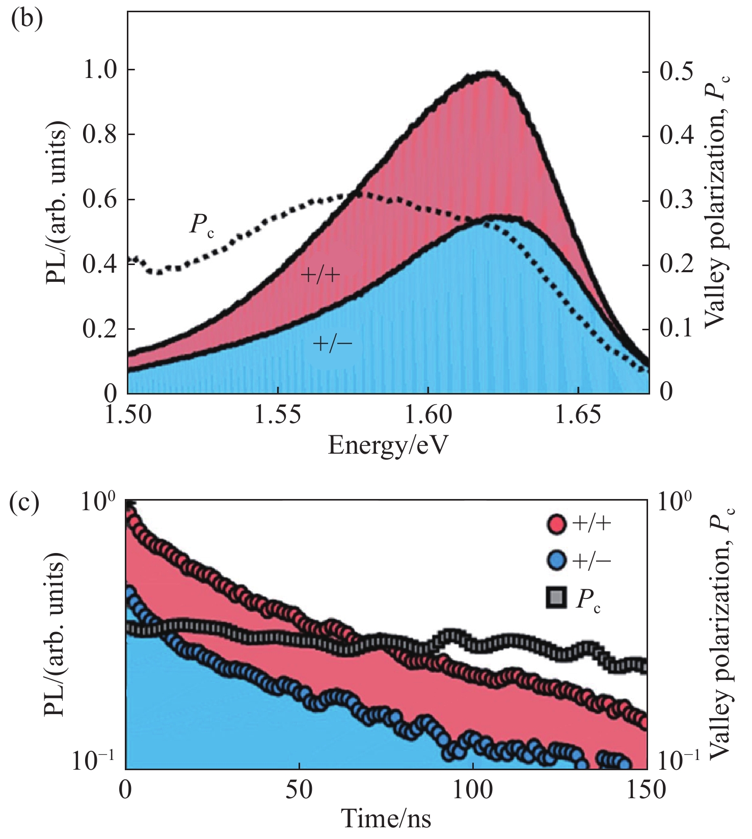
图 9 TMDCs缺陷对谷间散射的影响 。(a)理论计算得到的MoSe2的偏振荧光光谱,使用右旋光(蓝色)激发,得到左旋光和右旋光(红色)的荧光[79];(b) WSe2束缚态激子的积分荧光光谱和不同光子能量的谷偏振度[78];(c)WSe2束缚态激子瞬态荧光和谷偏振度随时间的变化[78]
Figure 9. The effect of defects on intervalley scattering in TMDCs. (a) Calculated PL spectrum of MoSe2 excited by right-handed light (blue line), observing PL from the left and the right (red line)[79]; (b) integrated PL spectrum of bound exciton in defective WSe2 and their degree of valley polarization[78]; (c) decay of PL and valley polarization degree of bound exciton in defective WSe2[78]
-
[1] NOVOSELOV K S, GEIM A K, MOROZOV S V, et al. Electric field effect in atomically thin carbon films[J]. Science, 2004, 306(5696): 666-669. doi: 10.1126/science.1102896 [2] HAN P, WANG X K, ZHANG Y. Time-resolved terahertz spectroscopy studies on 2D van der Waals materials[J]. Advanced Optical Materials, 2020, 8(3): 1900533. doi: 10.1002/adom.201900533 [3] MOUNET N, GIBERTINI M, SCHWALLER P, et al. Two-dimensional materials from high-throughput computational exfoliation of experimentally known compounds[J]. Nature Nanotechnology, 2018, 13(3): 246-252. doi: 10.1038/s41565-017-0035-5 [4] CASTELLANOS-GOMEZ A. Why all the fuss about 2D semiconductors?[J]. Nature Photonics, 2016, 10(4): 202-204. doi: 10.1038/nphoton.2016.53 [5] AJAYAN P, KIM P, BANERJEE K. Two-dimensional van der Waals materials[J]. Physics Today, 2016, 69(9): 38-44. doi: 10.1063/PT.3.3297 [6] BERKELBACH T C, REICHMAN D R. Optical and excitonic properties of atomically thin transition-metal dichalcogenides[J]. Annual Review of Condensed Matter Physics, 2018, 9(1): 379-396. doi: 10.1146/annurev-conmatphys-033117-054009 [7] GUO B, XIAO Q L, WANG SH H, et al. 2D layered materials: synthesis, nonlinear optical properties, and device applications[J]. Laser &Photonics Reviews, 2019, 13(12): 1800327. [8] KANG S, LEE D, KIM J, et al. 2D semiconducting materials for electronic and optoelectronic applications: potential and challenge[J]. 2D Materials, 2020, 7(2): 022003. doi: 10.1088/2053-1583/ab6267 [9] MUELLER T, MALIC E. Exciton physics and device application of two-dimensional transition metal dichalcogenide semiconductors[J]. npj 2D Materials and Applications, 2018, 2(1): 29. doi: 10.1038/s41699-018-0074-2 [10] TAN CH L, CAO X H, WU X J, et al. Recent advances in ultrathin two-dimensional nanomaterials[J]. Chemical Reviews, 2017, 117(9): 6225-6331. doi: 10.1021/acs.chemrev.6b00558 [11] XIA F N, WANG H, XIAO D, et al. Two-dimensional material nanophotonics[J]. Nature Photonics, 2014, 8(12): 899-907. doi: 10.1038/nphoton.2014.271 [12] MAK K F, LEE C, HONE J, et al. Atomically thin MoS2: A new direct-gap semiconductor[J]. Physical Review Letters, 2010, 105(13): 136805. doi: 10.1103/PhysRevLett.105.136805 [13] ROLDÁN R, SILVA-GUILLÉN J A, LÓPEZ-SANCHO M P, et al. Electronic properties of single-layer and multilayer transition metal dichalcogenides MX2 (M= Mo, W and X= S, Se)[J]. Annalen der Physik, 2014, 526(9-10): 347-357. doi: 10.1002/andp.201400128 [14] RUPPERT C, ASLAN O B, HEINZ T F. Optical properties and band gap of single- and few-layer MoTe2 crystals[J]. Nano Letters, 2014, 14(11): 6231-6236. doi: 10.1021/nl502557g [15] SPLENDIANI A, SUN L, ZHANG Y B, et al. Emerging photoluminescence in monolayer MoS2[J]. Nano Letters, 2010, 10(4): 1271-1275. doi: 10.1021/nl903868w [16] ZHAO W J, GHORANNEVIS Z, CHU L Q, et al. Evolution of electronic structure in atomically thin sheets of WS2 and WSe2[J]. ACS Nano, 2013, 7(1): 791-797. doi: 10.1021/nn305275h [17] CHERNIKOV A, BERKELBACH T C, HILL H M, et al. Exciton binding energy and nonhydrogenic rydberg series in monolayer WS2[J]. Physical Review Letters, 2014, 113(7): 076802. doi: 10.1103/PhysRevLett.113.076802 [18] MAK K F, HE K L, LEE C, et al. Tightly bound trions in monolayer MoS2[J]. Nature Materials, 2013, 12(3): 207-211. doi: 10.1038/nmat3505 [19] PLECHINGER G, NAGLER P, ARORA A, et al. Trion fine structure and coupled spin–valley dynamics in monolayer tungsten disulfide[J]. Nature Communications, 2016, 7(1): 12715. doi: 10.1038/ncomms12715 [20] ROSS J S, WU S F, YU H Y, et al. Electrical control of neutral and charged excitons in a monolayer semiconductor[J]. Nature Communications, 2013, 4(1): 1474. doi: 10.1038/ncomms2498 [21] STEINHOFF A, FLORIAN M, SINGH A, et al. Biexciton fine structure in monolayer transition metal dichalcogenides[J]. Nature Physics, 2018, 14(12): 1199-1204. doi: 10.1038/s41567-018-0282-x [22] YOU Y M, ZHANG X X, BERKELBACH T C, et al. Observation of biexcitons in monolayer WSe2[J]. Nature Physics, 2015, 11(6): 477-481. doi: 10.1038/nphys3324 [23] LI ZH P, WANG T M, LU ZH G, et al. Revealing the biexciton and trion-exciton complexes in BN encapsulated WSe2[J]. Nature Communications, 2018, 9(1): 3719. doi: 10.1038/s41467-018-05863-5 [24] KUMAR N, NAJMAEI S, CUI Q N, et al. Second harmonic microscopy of monolayer MoS2[J]. Physical Review B, 2013, 87(16): 161403. doi: 10.1103/PhysRevB.87.161403 [25] LI Y L, RAO Y, MAK K F, et al. Probing symmetry properties of few-layer MoS2 and h-BN by optical second-harmonic generation[J]. Nano Letters, 2013, 13(7): 3329-3333. doi: 10.1021/nl401561r [26] MALARD L M, ALENCAR T V, BARBOZA A P M, et al. Observation of intense second harmonic generation from MoS2 atomic crystals[J]. Physical Review B, 2013, 87(20): 201401. doi: 10.1103/PhysRevB.87.201401 [27] CAO T, WANG G, HAN W P, et al. Valley-selective circular dichroism of monolayer molybdenum disulphide[J]. Nature Communications, 2012, 3(1): 887. doi: 10.1038/ncomms1882 [28] MAK K F, HE K L, SHAN J, et al. Control of valley polarization in monolayer MoS2 by optical helicity[J]. Nature Nanotechnology, 2012, 7(8): 494-498. doi: 10.1038/nnano.2012.96 [29] ZENG H L, DAI J F, YAO W, et al. Valley polarization in MoS2 monolayers by optical pumping[J]. Nature Nanotechnology, 2012, 7(8): 490-493. doi: 10.1038/nnano.2012.95 [30] UBRIG N, PONOMAREV E, ZULTAK J, et al. Design of van der Waals interfaces for broad-spectrum optoelectronics[J]. Nature Materials, 2020, 19(3): 299-304. doi: 10.1038/s41563-019-0601-3 [31] RIVERA P, SCHAIBLEY J R, JONES A M, et al. Observation of long-lived interlayer excitons in monolayer MoSe2-WSe2 heterostructures[J]. Nature Communications, 2015, 6(1): 6242. doi: 10.1038/ncomms7242 [32] ALEXEEV E M, RUIZ-TIJERINA D A, DANOVICH M, et al. Resonantly hybridized excitons in Moire superlattices in van der Waals heterostructures[J]. Nature, 2019, 567(7746): 81-86. doi: 10.1038/s41586-019-0986-9 [33] JIN CH H, REGAN E C, YAN A M, et al. Observation of Moire excitons in WSe2/WS2 heterostructure superlattices[J]. Nature, 2019, 567(7746): 76-80. doi: 10.1038/s41586-019-0976-y [34] TRAN K, MOODY G, WU F CH, et al. Evidence for Moire excitons in van der Waals heterostructures[J]. Nature, 2019, 567(7746): 71-75. doi: 10.1038/s41586-019-0975-z [35] RADISAVLJEVIC B, RADENOVIC A, BRIVIO J, et al. Single-layer MoS2 transistors[J]. Nature Nanotechnology, 2011, 6(3): 147-150. doi: 10.1038/nnano.2010.279 [36] BAO W ZH, CAI X H, KIM D, et al. High mobility ambipolar MoS2 field-effect transistors: substrate and dielectric effects[J]. Applied Physics Letters, 2013, 102(4): 042104. doi: 10.1063/1.4789365 [37] BIE Y Q, GROSSO G, HEUCK M, et al. A MoTe2-based light-emitting diode and photodetector for silicon photonic integrated circuits[J]. Nature Nanotechnology, 2017, 12(12): 1124-1129. doi: 10.1038/nnano.2017.209 [38] XIE Y, ZHANG B, WANG SH X, et al. Ultrabroadband MoS2 photodetector with spectral response from 445 to 2717 nm[J]. Advanced Materials, 2017, 29(17): 1605972. doi: 10.1002/adma.201605972 [39] LIU CH H, CLARK G, FRYETT T, et al. Nanocavity integrated van der Waals heterostructure light-emitting tunneling diode[J]. Nano Letters, 2017, 17(1): 200-205. doi: 10.1021/acs.nanolett.6b03801 [40] PU J, TAKENOBU T. Monolayer transition metal dichalcogenides as light sources[J]. Advanced Materials, 2018, 30(33): 1707627. doi: 10.1002/adma.201707627 [41] GE X CH, MINKOV M, FAN SH H, et al. Laterally confined photonic crystal surface emitting laser incorporating monolayer tungsten disulfide[J]. npj 2D Materials and Applications, 2019, 3(1): 16. doi: 10.1038/s41699-019-0099-1 [42] LI Y ZH, ZHANG J X, HUANG D D, et al. Room-temperature continuous-wave lasing from monolayer molybdenum ditelluride integrated with a silicon nanobeam cavity[J]. Nature Nanotechnology, 2017, 12(10): 987-992. doi: 10.1038/nnano.2017.128 [43] PAIK E Y, ZHANG L, BURG G W, et al. Interlayer exciton laser of extended spatial coherence in atomically thin heterostructures[J]. Nature, 2019, 576(7785): 80-84. doi: 10.1038/s41586-019-1779-x [44] WU S F, BUCKLEY S, SCHAIBLEY J R, et al. Monolayer semiconductor nanocavity lasers with ultralow thresholds[J]. Nature, 2015, 520(7545): 69-72. doi: 10.1038/nature14290 [45] FAVRON A, GAUFRÈS E, FOSSARD F, et al. Photooxidation and quantum confinement effects in exfoliated black phosphorus[J]. Nature Materials, 2015, 14(8): 826-832. doi: 10.1038/nmat4299 [46] NACLERIO A E, ZAKHAROV D N, KUMAR J, et al. Visualizing oxidation mechanisms in few-layered black phosphorus via in situ transmission electron microscopy[J]. ACS Applied Materials &Interfaces, 2020, 12(13): 15844-15854. [47] NAN H Y, GUO S J, CAI SH, et al. Producing air-stable inse nanosheet through mild oxygen plasma treatment[J]. Semiconductor Science and Technology, 2018, 33(7): 074002. doi: 10.1088/1361-6641/aac3e6 [48] HUANG Y, SUTTER E, SHI N N, et al. Reliable exfoliation of large-area high-quality flakes of graphene and other two-dimensional materials[J]. ACS Nano, 2015, 9(11): 10612-10620. doi: 10.1021/acsnano.5b04258 [49] HUANG Y, PAN Y H, YANG R, et al. Universal mechanical exfoliation of large-area 2D crystals[J]. Nature Communications, 2020, 11(1): 2453. doi: 10.1038/s41467-020-16266-w [50] LIU F, WU W J, BAI Y S, et al. Disassembling 2D van der Waals crystals into macroscopic monolayers and reassembling into artificial lattices[J]. Science, 2020, 367(6480): 903-906. doi: 10.1126/science.aba1416 [51] SHIM J, BAE S H, KONG W, et al. Controlled crack propagation for atomic precision handling of wafer-scale two-dimensional materials[J]. Science, 2018, 362(6415): 665-670. doi: 10.1126/science.aat8126 [52] BERNAL M M, ÁLVAREZ L, GIOVANELLI E, et al. Luminescent transition metal dichalcogenide nanosheets through one-step liquid phase exfoliation[J]. 2D Materials, 2016, 3(3): 035014. doi: 10.1088/2053-1583/3/3/035014 [53] JAWAID A, NEPAL D, PARK K, et al. Mechanism for liquid phase exfoliation of MoS2[J]. Chemistry of Materials, 2016, 28(1): 337-348. doi: 10.1021/acs.chemmater.5b04224 [54] QI ZH H, HU Y, JIN ZH, et al. Tuning the liquid-phase exfoliation of arsenic nanosheets by interaction with various solvents[J]. Physical Chemistry Chemical Physics, 2019, 21(23): 12087-12090. doi: 10.1039/C9CP01052A [55] SHREE S, GEORGE A, LEHNERT T, et al. High optical quality of MoS2 monolayers grown by chemical vapor deposition[J]. 2D Materials, 2019, 7(1): 015011. doi: 10.1088/2053-1583/ab4f1f [56] YU H, LIAO M ZH, ZHAO W J, et al. Wafer-scale growth and transfer of highly-oriented monolayer MoS2 continuous films[J]. ACS Nano, 2017, 11(12): 12001-12007. doi: 10.1021/acsnano.7b03819 [57] HU Y, CHEN T, WANG X Q, et al. Controlled growth and photoconductive properties of hexagonal SnS2 nanoflakes with mesa-shaped atomic steps[J]. Nano Research, 2017, 10(4): 1434-1447. doi: 10.1007/s12274-017-1525-3 [58] CHEN M W, OVCHINNIKOV D, LAZAR S, et al. Highly oriented atomically thin ambipolar MoSe2 grown by molecular beam epitaxy[J]. ACS Nano, 2017, 11(6): 6355-6361. doi: 10.1021/acsnano.7b02726 [59] HU Y, QI ZH H, LU J Y, et al. Van der Waals epitaxial growth and interfacial passivation of two-dimensional single-crystalline few-layer gray arsenic nanoflakes[J]. Chemistry of Materials, 2019, 31(12): 4524-4535. doi: 10.1021/acs.chemmater.9b01151 [60] FU D Y, ZHAO X X, ZHANG Y Y, et al. Molecular beam epitaxy of highly crystalline monolayer molybdenum disulfide on hexagonal boron nitride[J]. Journal of the American Chemical Society, 2017, 139(27): 9392-9400. doi: 10.1021/jacs.7b05131 [61] NAKANO M, WANG Y, KASHIWABARA Y, et al. Layer-by-layer epitaxial growth of scalable WSe2 on sapphire by molecular beam epitaxy[J]. Nano Letters, 2017, 17(9): 5595-5599. doi: 10.1021/acs.nanolett.7b02420 [62] WANG H N, ZHANG CH J, RANA F. Ultrafast dynamics of defect-assisted electron-hole recombination in monolayer MoS2[J]. Nano Letters, 2015, 15(1): 339-345. doi: 10.1021/nl503636c [63] LI L Q, LIN M F, ZHANG X, et al. Phonon-suppressed auger scattering of charge carriers in defective two-dimensional transition metal dichalcogenides[J]. Nano Letters, 2019, 19(9): 6078-6086. doi: 10.1021/acs.nanolett.9b02005 [64] LI Y L, LIU W, WANG Y K, et al. Ultrafast electron cooling and decay in monolayer WS2 revealed by time- and energy-resolved photoemission electron microscopy[J]. Nano Letters, 2020, 20(5): 3747-3753. doi: 10.1021/acs.nanolett.0c00742 [65] LIU H, WANG CH, ZUO ZH G, et al. Direct visualization of exciton transport in defective few-layer WS2 by ultrafast microscopy[J]. Advanced Materials, 2020, 32(2): 1906540. doi: 10.1002/adma.201906540 [66] LI L SH, CARTER E A. Defect-mediated charge-carrier trapping and nonradiative recombination in WSe2 monolayers[J]. Journal of the American Chemical Society, 2019, 141(26): 10451-10461. doi: 10.1021/jacs.9b04663 [67] AMANI M, LIEN D H, KIRIYA D, et al. Near-unity photoluminescence quantum yield in MoS2[J]. Science, 2015, 350(6264): 1065-1068. doi: 10.1126/science.aad2114 [68] WU ZH T, LUO ZH ZH, SHEN Y T, et al. Defects as a factor limiting carrier mobility in WSe2: a spectroscopic investigation[J]. Nano Research, 2016, 9(12): 3622-3631. doi: 10.1007/s12274-016-1232-5 [69] TOSUN M, CHAN L, AMANI M, et al. Air-stable n-doping of WSe2 by anion vacancy formation with mild plasma treatment[J]. ACS Nano, 2016, 10(7): 6853-6860. doi: 10.1021/acsnano.6b02521 [70] CHEE S S, LEE W J, JO Y R, et al. Atomic vacancy control and elemental substitution in a monolayer molybdenum disulfide for high performance optoelectronic device arrays[J]. Advanced Functional Materials, 2020, 30(11): 1908147. doi: 10.1002/adfm.201908147 [71] YANG J, KAWAI H, WONG C P Y, et al. Electrical doping effect of vacancies on monolayer MoS2[J]. The Journal of Physical Chemistry C, 2019, 123(5): 2933-2939. doi: 10.1021/acs.jpcc.8b10496 [72] CHEE S S, LEE J H, LEE K, et al. Defect-assisted contact property enhancement in a molybdenum disulfide monolayer[J]. ACS Applied Materials &Interfaces, 2020, 12(3): 4129-4134. [73] XIE Y, WU E X, HU R X, et al. Enhancing electronic and optoelectronic performances of tungsten diselenide by plasma treatment[J]. Nanoscale, 2018, 10(26): 12436-12444. doi: 10.1039/C8NR02668H [74] YIN L, HE P, CHENG R, et al. Robust trap effect in transition metal dichalcogenides for advanced multifunctional devices[J]. Nature Communications, 2019, 10(1): 4133. doi: 10.1038/s41467-019-12200-x [75] KOPERSKI M, NOGAJEWSKI K, ARORA A, et al. Single photon emitters in exfoliated WSe2 structures[J]. Nature Nanotechnology, 2015, 10(6): 503-506. doi: 10.1038/nnano.2015.67 [76] HE Y M, CLARK G, SCHAIBLEY J R, et al. Single quantum emitters in monolayer semiconductors[J]. Nature Nanotechnology, 2015, 10(6): 497-502. doi: 10.1038/nnano.2015.75 [77] SRIVASTAVA A, SIDLER M, ALLAIN A V, et al. Optically active quantum dots in monolayer WSe2[J]. Nature Nanotechnology, 2015, 10(6): 491-496. doi: 10.1038/nnano.2015.60 [78] MOODY G, TRAN K, LU X B, et al. Microsecond valley lifetime of defect-bound excitons in monolayer WSe2[J]. Physical Review Letters, 2018, 121(5): 057403. doi: 10.1103/PhysRevLett.121.057403 [79] REFAELY-ABRAMSON S, QIU D Y, LOUIE S G, et al. Defect-induced modification of low-lying excitons and valley selectivity in monolayer transition metal dichalcogenides[J]. Physical Review Letters, 2018, 121(16): 167402. doi: 10.1103/PhysRevLett.121.167402 [80] WANG Q SH, GE SH F, LI X, et al. Valley carrier dynamics in monolayer molybdenum disulfide from helicity-resolved ultrafast pump–probe spectroscopy[J]. ACS Nano, 2013, 7(12): 11087-11093. doi: 10.1021/nn405419h [81] WANG SH SH, ROBERTSON A, WARNER J H. Atomic structure of defects and dopants in 2D layered transition metal dichalcogenides[J]. Chemical Society Reviews, 2018, 47(17): 6764-6794. doi: 10.1039/C8CS00236C [82] WU ZH T, NI ZH H. Spectroscopic investigation of defects in two-dimensional materials[J]. Nanophotonics, 2017, 6(6): 1219-1237. doi: 10.1515/nanoph-2016-0151 [83] JIANG J, XU T, LU J P, et al. Defect engineering in 2D materials: precise manipulation and improved functionalities[J]. Research, 2019, 2019: 4641739. [84] LIN ZH, CARVALHO B R, KAHN E, et al. Defect engineering of two-dimensional transition metal dichalcogenides[J]. 2D Materials, 2016, 3(2): 022002. doi: 10.1088/2053-1583/3/2/022002 [85] ZHOU W, ZOU X L, NAJMAEI S, et al. Intrinsic structural defects in monolayer molybdenum disulfide[J]. Nano Letters, 2013, 13(6): 2615-2622. doi: 10.1021/nl4007479 [86] AMANI M, TAHERI P, ADDOU R, et al. Recombination kinetics and effects of superacid treatment in sulfur- and selenium-based transition metal dichalcogenides[J]. Nano Letters, 2016, 16(4): 2786-2791. doi: 10.1021/acs.nanolett.6b00536 [87] HONG J H, HU ZH X, PROBERT M, et al. Exploring atomic defects in molybdenum disulphide monolayers[J]. Nature Communications, 2015, 6(1): 6293. doi: 10.1038/ncomms7293 [88] SCHULER B, QIU D Y, REFAELY-ABRAMSON S, et al. Large spin-orbit splitting of deep in-gap defect states of engineered sulfur vacancies in monolayer WS2[J]. Physical Review Letters, 2019, 123(7): 076801. doi: 10.1103/PhysRevLett.123.076801 [89] CHEN P, SHANG J M, YANG Y, et al. Annealing tunes interlayer coupling and optoelectronic property of bilayer SnSe2/MoSe2 heterostructures[J]. Applied Surface Science, 2017, 419: 460-464. doi: 10.1016/j.apsusc.2017.04.244 [90] HE ZH Y, WANG X CH, XU W SH, et al. Revealing defect-state photoluminescence in monolayer WS2 by cryogenic laser processing[J]. ACS Nano, 2016, 10(6): 5847-5855. doi: 10.1021/acsnano.6b00714 [91] PETŐ J, OLLÁR T, VANCSÓ P, et al. Spontaneous doping of the basal plane of MoS2 single layers through oxygen substitution under ambient conditions[J]. Nature Chemistry, 2018, 10(12): 1246-1251. doi: 10.1038/s41557-018-0136-2 [92] BARJA S, REFAELY-ABRAMSON S, SCHULER B, et al. Identifying substitutional oxygen as a prolific point defect in monolayer transition metal dichalcogenides[J]. Nature Communications, 2019, 10(1): 3382. doi: 10.1038/s41467-019-11342-2 [93] SCHULER B, LEE J H, KASTL C, et al. How substitutional point defects in two-dimensional WS2 induce charge localization, spin-orbit splitting, and strain[J]. ACS Nano, 2019, 13(9): 10520-10534. doi: 10.1021/acsnano.9b04611 [94] AGHAJANIAN M, SCHULER B, COCHRANE K A, et al. Resonant and bound states of charged defects in two-dimensional semiconductors[J]. Physical Review B, 2020, 101(8): 081201. doi: 10.1103/PhysRevB.101.081201 [95] CHEN M, HAM H, WI S, et al. Multibit data storage states formed in plasma-treated MoS2 transistors[J]. Acs Nano, 2014, 8(4): 4023-4032. [96] HU Z H, WU ZH T, HAN CH, et al. Two-dimensional transition metal dichalcogenides: Interface and defect engineering[J]. Chemical Society Reviews, 2018, 47(9): 3100-3128. doi: 10.1039/C8CS00024G [97] ZAN R, RAMASSE Q M, JALIL R, et al. Control of radiation damage in MoS2 by graphene encapsulation[J]. ACS Nano, 2013, 7(11): 10167-10174. doi: 10.1021/nn4044035 [98] KOMSA H P, KOTAKOSKI J, KURASCH S, et al. Two-dimensional transition metal dichalcogenides under electron irradiation: defect production and doping[J]. Physical Review Letters, 2012, 109(3): 035503. doi: 10.1103/PhysRevLett.109.035503 [99] WALKER II R C, SHI T, SILVA E C, et al. Radiation effects on two-dimensional materials[J]. Physica Status Solidi (A) , 2016, 213(12): 3065-3077. doi: 10.1002/pssa.201600395 [100] ZHAO G Y, DENG H, TYREE N, et al. Recent progress on irradiation-induced defect engineering of two-dimensional 2H-MoS2 few layers[J]. Applied Sciences, 2019, 9(4): 678. doi: 10.3390/app9040678 [101] CHOW P K, JACOBS-GEDRIM R B, GAO J, et al. Defect-induced photoluminescence in monolayer semiconducting transition metal dichalcogenides[J]. ACS Nano, 2015, 9(2): 1520-1527. doi: 10.1021/nn5073495 [102] TONGAY S, SUH J, ATACA C, et al. Defects activated photoluminescence in two-dimensional semiconductors: interplay between bound, charged and free excitons[J]. Scientific Reports, 2013, 3: 2657. doi: 10.1038/srep02657 [103] WU ZH T, ZHAO W W, JIANG J, et al. Defect activated photoluminescence in WSe2 monolayer[J]. The Journal of Physical Chemistry C, 2017, 121(22): 12294-12299. doi: 10.1021/acs.jpcc.7b03585 [104] MITTERREITER E, SCHULER B, COCHRANE K A, et al. Atomistic positioning of defects in helium ion treated single layer MoS2[J]. Nano Letters, 2020, 20(6): 4437-4444. [105] MENG J L, WEI ZH, TANG J, et al. Employing defected monolayer MoS2 as charge storage materials[J]. Nanotechnology, 2020, 31(23): 235710. doi: 10.1088/1361-6528/ab7c47 [106] ZHANG SH, WANG CH G, LI M Y, et al. Defect structure of localized excitons in a WSe2 monolayer[J]. Physical Review Letters, 2017, 119(4): 046101. doi: 10.1103/PhysRevLett.119.046101 [107] ZHENG Y J, CHEN Y F, HUANG Y L, et al. Point defects and localized excitons in 2D WSe2[J]. ACS Nano, 2019, 13(5): 6050-6059. doi: 10.1021/acsnano.9b02316 [108] LEE Y, YUN S J, KIM Y, et al. Near-field spectral mapping of individual exciton complexes of monolayer WS2 correlated with local defects and charge population[J]. Nanoscale, 2017, 9(6): 2272-2278. doi: 10.1039/C6NR08813A [109] KUMAR R, VERZHBITSKIY I, EDA G. Strong optical absorption and photocarrier relaxation in 2-D semiconductors[J]. IEEE Journal of Quantum Electronics, 2015, 51(10): 0600206. [110] GREBEN K, ARORA S, HARATS M G, et al. Intrinsic and extrinsic defect-related excitons in TMDCs[J]. Nano Letters, 2020, 20(4): 2544-2550. doi: 10.1021/acs.nanolett.9b05323 [111] JADCZAK J, KUTROWSKA-GIRZYCKA J, KAPUŚCIŃSKI P, et al. Probing of free and localized excitons and trions in atomically thin WSe2, WS2, MoSe2 and MoS2 in photoluminescence and reflectivity experiments[J]. Nanotechnology, 2017, 28(39): 395702. doi: 10.1088/1361-6528/aa87d0 [112] SHANG J ZH, CONG CH X, SHEN X N, et al. Revealing electronic nature of broad bound exciton bands in two-dimensional semiconducting WS2 and MoS2[J]. Physical Review Materials, 2017, 1(7): 074001. doi: 10.1103/PhysRevMaterials.1.074001 [113] WIERZBOWSKI J, KLEIN J, SIGGER F, et al. Direct exciton emission from atomically thin transition metal dichalcogenide heterostructures near the lifetime limit[J]. Scientific Reports, 2017, 7(1): 12383. doi: 10.1038/s41598-017-09739-4 [114] YU Y, DANG J CH, QIAN CH J, et al. Many-body effect of mesoscopic localized states in MoS2 monolayer[J]. Physical Review Materials, 2019, 3(5): 051001. doi: 10.1103/PhysRevMaterials.3.051001 [115] CAROZO V, WANG Y X, FUJISAWA K, et al. Optical identification of sulfur vacancies: Bound excitons at the edges of monolayer tungsten disulfide[J]. Science Advances, 2017, 3(4): e1602813. doi: 10.1126/sciadv.1602813 [116] KATO T, KANEKO T. Optical detection of a highly localized impurity state in monolayer tungsten disulfide[J]. ACS Nano, 2014, 8(12): 12777-12785. doi: 10.1021/nn5059858 [117] MOLAS M R, NOGAJEWSKI K, SLOBODENIUK A O, et al. The optical response of monolayer, few-layer and bulk tungsten disulfide[J]. Nanoscale, 2017, 9(35): 13128-13141. doi: 10.1039/C7NR04672C [118] GORDO V O, BALANTA M A G, GOBATO Y G, et al. Revealing the nature of low-temperature photoluminescence peaks by laser treatment in van der Waals epitaxially grown WS2 monolayers[J]. Nanoscale, 2018, 10(10): 4807-4815. doi: 10.1039/C8NR00719E [119] VENANZI T, ARORA H, ERBE A, et al. Exciton localization in MoSe2 monolayers induced by adsorbed gas molecules[J]. Applied Physics Letters, 2019, 114(17): 172106. doi: 10.1063/1.5094118 [120] HE Z Y, ZHAO R, CHEN X F, et al. Defect engineering in single-layer MoS2 using heavy ion irradiation[J]. ACS Applied Materials &Interfaces, 2018, 10(49): 42524-42533. [121] LEE C, JEONG B G, YUN S J, et al. Unveiling defect-related raman mode of monolayer WS2 via tip-enhanced resonance raman scattering[J]. ACS Nano, 2018, 12(10): 9982-9990. doi: 10.1021/acsnano.8b04265 [122] MIGNUZZI S, POLLARD A J, BONINI N, et al. Effect of disorder on raman scattering of single-layer MoS2[J]. Physical Review B, 2015, 91(19): 195411. doi: 10.1103/PhysRevB.91.195411 [123] SHI W, LIN M L, TAN Q H, et al. Raman and photoluminescence spectra of two-dimensional nanocrystallites of monolayer WS2 and WSe2[J]. 2D Materials, 2016, 3(2): 025016. doi: 10.1088/2053-1583/3/2/025016 [124] SHI W, ZHANG X, LI X L, et al. Phonon confinement effect in two-dimensional nanocrystallites of monolayer MoS2 to probe phonon dispersion trends away from brillouin-zone center[J]. Chinese Physics Letters, 2016, 33(5): 057801. doi: 10.1088/0256-307X/33/5/057801 [125] ZHANG X, QIAO X F, SHI W, et al. Phonon and raman scattering of two-dimensional transition metal dichalcogenides from monolayer, multilayer to bulk material[J]. Chemical Society Reviews, 2015, 44(9): 2757-2785. doi: 10.1039/C4CS00282B [126] WANG J Y, VERZHBITSKIY I, EDA G. Electroluminescent devices based on 2D semiconducting transition metal dichalcogenides[J]. Advanced Materials, 2018, 30(47): e1802687. doi: 10.1002/adma.201802687 [127] PAUR M, MOLINA-MENDOZA A J, BRATSCHITSCH R, et al. Electroluminescence from multi-particle exciton complexes in transition metal dichalcogenide semiconductors[J]. Nature Communications, 2019, 10(1): 1709. doi: 10.1038/s41467-019-09781-y [128] POSPISCHIL A, FURCHI M M, MUELLER T. Solar-energy conversion and light emission in an atomic monolayer p-n diode[J]. Nature Nanotechnology, 2014, 9(4): 257-261. doi: 10.1038/nnano.2014.14 [129] ROSS J S, RIVERA P, SCHAIBLEY J, et al. Interlayer exciton optoelectronics in a 2D heterostructure p-n junction[J]. Nano Letters, 2017, 17(2): 638-643. doi: 10.1021/acs.nanolett.6b03398 [130] CLARK G, SCHAIBLEY J R, ROSS J, et al. Single defect light-emitting diode in a van der Waals heterostructure[J]. Nano Letters, 2016, 16(6): 3944-3948. doi: 10.1021/acs.nanolett.6b01580 [131] SCHWARZ S, KOZIKOV A, WITHERS F, et al. Electrically pumped single-defect light emitters in WSe2[J]. 2D Materials, 2016, 3(2): 025038. doi: 10.1088/2053-1583/3/2/025038 [132] PALACIOS-BERRAQUERO C, BARBONE M, KARA D M, et al. Atomically thin quantum light-emitting diodes[J]. Nature Communications, 2016, 7: 12978. doi: 10.1038/ncomms12978 [133] SCHULER B, COCHRANE K A, KASTL C, et al. Electrically driven photon emission from individual atomic defects in monolayer WS2[J]. Science advances, 2020, 6(38): eabb5988. doi: 10.1126/sciadv.abb5988 [134] KIM H, LIEN D H, AMANI M, et al. Highly stable near-unity photoluminescence yield in monolayer MoS2 by fluoropolymer encapsulation and superacid treatment[J]. ACS Nano, 2017, 11(5): 5179-5185. doi: 10.1021/acsnano.7b02521 [135] GOODMAN A J, WILLARD A P, TISDALE W A. Exciton trapping is responsible for the long apparent lifetime in acid-treated MoS2[J]. Physical Review B, 2017, 96(12): 121404. doi: 10.1103/PhysRevB.96.121404 [136] BRETSCHER H M, LI Z J, XIAO J, et al.. The bright side of defects in MoS2 and WS2 and a generalizable chemical treatment protocol for defect passivation[J]. arXiv preprint arXiv, 2020, 2002.03956. [137] TANOH A O A, ALEXANDER-WEBBER J, XIAO J, et al. Enhancing photoluminescence and mobilities in WS2 monolayers with oleic acid ligands[J]. Nano Letters, 2019, 19(9): 6299-6307. doi: 10.1021/acs.nanolett.9b02431 [138] HAN H V, LU A Y, LU L S, et al. Photoluminescence enhancement and structure repairing of monolayer MoSe2 by hydrohalic acid treatment[J]. ACS Nano, 2016, 10(1): 1454-1461. doi: 10.1021/acsnano.5b06960 [139] TANOH A O A, XIAO J, ALEXANDER-WEBBER J, et al.. Giant photoluminescence enhancement in MoSe2 monolayers treated with oleic acid ligands[J]. arXiv preprint arXiv, 2006.04505, 2020. [140] KIM H, AHN G H, CHO J, et al. Synthetic WSe2 monolayers with high photoluminescence quantum yield[J]. Science Advances, 2019, 5(1): eaau4728. doi: 10.1126/sciadv.aau4728 [141] LIEN D H, UDDIN S Z, YEH M, et al. Electrical suppression of all nonradiative recombination pathways in monolayer semiconductors[J]. Science, 2019, 364(6439): 468-471. doi: 10.1126/science.aaw8053 [142] STRIKHA M V, KURCHAK A I, MOROZOVSKA A N. Gate-voltage control of quantum yield in monolayer transition-metal dichalcogenide[J]. Physical Review Applied, 2020, 13(1): 014040. doi: 10.1103/PhysRevApplied.13.014040 [143] ATALLAH T L, WANG J, BOSCH M, et al. Electrostatic screening of charged defects in monolayer MoS2[J]. Journal of Physical Chemistry Letters, 2017, 8(10): 2148-2152. doi: 10.1021/acs.jpclett.7b00710 [144] NAN H Y, WANG Z L, WANG W H, et al. Strong photoluminescence enhancement of MoS2 through defect engineering and oxygen bonding[J]. ACS Nano, 2014, 8(6): 5738-5745. doi: 10.1021/nn500532f [145] LU J P, CARVALHO A, CHAN X K, et al. Atomic healing of defects in transition metal dichalcogenides[J]. Nano Letters, 2015, 15(5): 3524-3532. doi: 10.1021/acs.nanolett.5b00952 [146] OH H M, HAN G H, KIM H, et al. Photochemical reaction in monolayer MoS2 via correlated photoluminescence, raman spectroscopy, and atomic force microscopy[J]. ACS Nano, 2016, 10(5): 5230-5236. doi: 10.1021/acsnano.6b00895 [147] ARDEKANI H, YOUNTS R, YU Y L, et al. Reversible photoluminescence tuning by defect passivation via laser irradiation on aged monolayer MoS2[J]. ACS Applied Materials &Interfaces, 2019, 11(41): 38240-38246. [148] LEE Y, GHIMIRE G, ROY S, et al. Impeding exciton–exciton annihilation in monolayer WS2 by laser irradiation[J]. ACS Photonics, 2018, 5(7): 2904-2911. doi: 10.1021/acsphotonics.8b00249 [149] VENKATAKRISHNAN A, CHUA H, TAN P, et al. Microsteganography on WS2 monolayers tailored by direct laser painting[J]. ACS Nano, 2017, 11(1): 713-720. doi: 10.1021/acsnano.6b07118 [150] SIVARAM S V, HANBICKI A T, ROSENBERGER M R, et al. Spatially selective enhancement of photoluminescence in MoS2 by exciton-mediated adsorption and defect passivation[J]. ACS Applied Materials &Interfaces, 2019, 11(17): 16147-16155. [151] WANG W F, SHU H B, WANG J, et al. Defect passivation and photoluminescence enhancement of monolayer MoS2 crystals through sodium halide-assisted chemical vapor deposition growth[J]. ACS Applied Materials &Interfaces, 2020, 12(8): 9563-9571. [152] ZHU Y, YI H, HAO Q Y, et al. Scalable synthesis and defect modulation of large monolayer WS2 via annealing in H2S atmosphere/thiol treatment to enhance photoluminescence[J]. Applied Surface Science, 2019, 485: 101-107. doi: 10.1016/j.apsusc.2019.04.168 [153] NIE ZH G, LONG R, SUN L F, et al. Ultrafast carrier thermalization and cooling dynamics in few-layer MoS2[J]. ACS Nano, 2014, 8(10): 10931-10940. doi: 10.1021/nn504760x [154] CEBALLOS F, CUI Q N, BELLUS M Z, et al. Exciton formation in monolayer transition metal dichalcogenides[J]. Nanoscale, 2016, 8(22): 11681-11688. doi: 10.1039/C6NR02516A [155] SHI H Y, YAN R S, BERTOLAZZI S, et al. Exciton dynamics in suspended monolayer and few-layer MoS2 2D crystals[J]. ACS Nano, 2013, 7(2): 1072-1080. doi: 10.1021/nn303973r [156] ZIPFEL J, KULIG M, PEREA-CAUSÍN R, et al. Exciton diffusion in monolayer semiconductors with suppressed disorder[J]. Physical Review B, 2020, 101(11): 115430. doi: 10.1103/PhysRevB.101.115430 [157] LIU H, WANG CH, LIU D M, et al. Neutral and defect-induced exciton annihilation in defective monolayer WS2[J]. Nanoscale, 2019, 11(16): 7913-7920. doi: 10.1039/C9NR00967A [158] KAR S, SU Y, NAIR R R, et al. Probing photoexcited carriers in a few-layer MoS2 laminate by time-resolved optical pump-terahertz probe spectroscopy[J]. ACS Nano, 2015, 9(12): 12004-12010. doi: 10.1021/acsnano.5b04804 [159] CHEN K, GHOSH R, MENG X H, et al. Experimental evidence of exciton capture by mid-gap defects in CVD grown monolayer MoSe2[J]. npj 2D Materials and Applications, 2017, 1(1): 15. doi: 10.1038/s41699-017-0019-1 [160] CHU ZH D, WANG CH Y, QUAN J M, et al. Unveiling defect-mediated carrier dynamics in monolayer semiconductors by spatiotemporal microwave imaging[J]. Proceedings of the National Academy of Sciences of the United States of America, 2020, 117(25): 13908-13913. doi: 10.1073/pnas.2004106117 [161] HEIN P, STANGE A, HANFF K, et al. Momentum-resolved hot electron dynamics at the 2H-MoS2 surface[J]. Physical Review B, 2016, 94(20): 205406. doi: 10.1103/PhysRevB.94.205406 [162] KASTL C, KOCH R J, CHEN C T, et al. Effects of defects on band structure and excitons in WS2 revealed by nanoscale photoemission spectroscopy[J]. ACS Nano, 2019, 13(2): 1284-1291. [163] SUN Q, YU H, UENO K, et al. Dissecting the few-femtosecond dephasing time of dipole and quadrupole modes in gold nanoparticles using polarized photoemission electron microscopy[J]. ACS Nano, 2016, 10(3): 3835-3842. doi: 10.1021/acsnano.6b00715 [164] YU H, SUN Q, UENO K, et al. Exploring coupled plasmonic nanostructures in the near field by photoemission electron microscopy[J]. ACS Nano, 2016, 10(11): 10373-10381. doi: 10.1021/acsnano.6b06206 [165] ULSTRUP S, ČABO A G, MIWA J A, et al. Ultrafast band structure control of a two-dimensional heterostructure[J]. ACS Nano, 2016, 10(6): 6315-6322. doi: 10.1021/acsnano.6b02622 [166] ČABO A G, MIWA J A, GRONBORG S S, et al. Observation of ultrafast free carrier dynamics in single layer MoS2[J]. Nano Letters, 2015, 15(9): 5883-5887. doi: 10.1021/acs.nanolett.5b01967 [167] JULIEN M, MICHAEL K. L. M, CHAKRADHAR S, et al. Directly visualizing the momentum-forbidden dark excitons and their dynamics in atomically thin semiconductors[J]. Science, 2020, 370(6521): 1199-1204. doi: 10.1126/science.aba1029 [168] JOHANNSEN J C, ULSTRUP S, CILENTO F, et al. Direct view of hot carrier dynamics in graphene[J]. Physical Review Letters, 2013, 111(2): 027403. doi: 10.1103/PhysRevLett.111.027403 [169] BERTONI R, NICHOLSON C W, WALDECKER L, et al. Generation and evolution of spin-, valley-, and layer-polarized excited carriers in inversion-symmetric WSe2[J]. Physical Review Letters, 2016, 117(27): 277201. doi: 10.1103/PhysRevLett.117.277201 [170] BEYER H, ROHDE G, ČABO A G, et al. 80% valley polarization of free carriers in singly oriented single-layer WS2 on Au (111)[J]. Physical Review Letters, 2019, 123(23): 236802. doi: 10.1103/PhysRevLett.123.236802 [171] MAN M K L, MARGIOLAKIS A, DECKOFF-JONES S, et al. Imaging the motion of electrons across semiconductor heterojunctions[J]. Nature Nanotechnology, 2017, 12(1): 36-40. doi: 10.1038/nnano.2016.183 [172] LI Y L, SUN Q, ZU SH, et al. Correlation between near-field enhancement and dephasing time in plasmonic dimers[J]. Physical Review Letters, 2020, 124(16): 163901. doi: 10.1103/PhysRevLett.124.163901 [173] WANG L, XU C, LI M Y, et al. Unraveling spatially heterogeneous ultrafast carrier dynamics of single-layer WSe2 by femtosecond time-resolved photoemission electron microscopy[J]. Nano Letters, 2018, 18(8): 5172-5178. doi: 10.1021/acs.nanolett.8b02103 [174] DOHERTY T A S, WINCHESTER A J, MACPHERSON S, et al. Performance-limiting nanoscale trap clusters at grain junctions in halide perovskites[J]. Nature, 2020, 580(7803): 360-366. doi: 10.1038/s41586-020-2184-1 [175] SOBOTA J A, YANG S, ANALYTIS J G, et al. Ultrafast optical excitation of a persistent surface-state population in the topological insulator Bi2Se3[J]. Physical Review Letters, 2012, 108(11): 117403. doi: 10.1103/PhysRevLett.108.117403 [176] GOODMAN A J, LIEN D H, AHN G H, et al. Substrate-dependent exciton diffusion and annihilation in chemically treated MoS2 and WS2[J]. The Journal of Physical Chemistry C, 2020, 124(22): 12175-12184. doi: 10.1021/acs.jpcc.0c04000 [177] KAASBJERG K, MARTINY J H J, LOW T, et al. Symmetry-forbidden intervalley scattering by atomic defects in monolayer transition-metal dichalcogenides[J]. Physical Review B, 2017, 96(24): 241411. doi: 10.1103/PhysRevB.96.241411 -

 下载:
下载:


计量
- 文章访问数: 5484
- HTML全文浏览量: 1159
- PDF下载量: 560
- 被引次数: 0
