


Fabrication and optoelectronic characterization of suspended In2O3 nanowire transistors
doi: 10.37188/CO.2020-0062
-
摘要: 一维(1D)半导体纳米线在纳米电子学和纳米光子学中表现出色。然而,纳米线晶体管的电特性对纳米线与衬底之间的相互作用非常敏感,而优化器件结构可以改善纳米线晶体管的电学和光电检测性能。本文报道了通过一步式光刻技术制造的悬浮式In2O3纳米线晶体管,显示出54.6 cm2V−1s−1的高迁移率和241.5 mVdec−1的低亚阈值摆幅。作为紫外光电探测器,光电晶体管显示出极低的暗电流(~10−13 A)和高响应度1.6×10⁵ A•W−1。悬浮晶体管的沟道材料的这种简单而有效的制备方法可广泛用于制造高性能微纳米器件。Abstract: One-dimensional (1D) semiconductor nanowires have shown outstanding performance in nano-electronics and nano-photonics. However, the electrical properties of the nanowire transistors are very sensitive to interactions between the nanowires and substrates. Optimizing the device structure can improve the electrical and photodetection performance of nanowire transistors. We report a suspended In2O3 nanowire transistor fabricated by one-step lithography, showing a high mobility of 54.6 cm2V−1s−1 and a low subthreshold swing of 241.5 mVdec−1. As an ultraviolet photodetector, the phototransistor shows an extremely low dark current (~10−13 A) and a high responsivity of 1.6×10⁵ A•W−1. This simple and effective method of suspending the channel material of a transistor can be widely used in manufacturing high-performance micro-nano devices.
-
Key words:
- nanowire /
- In2O3 /
- suspension device /
- UV photodetector
-
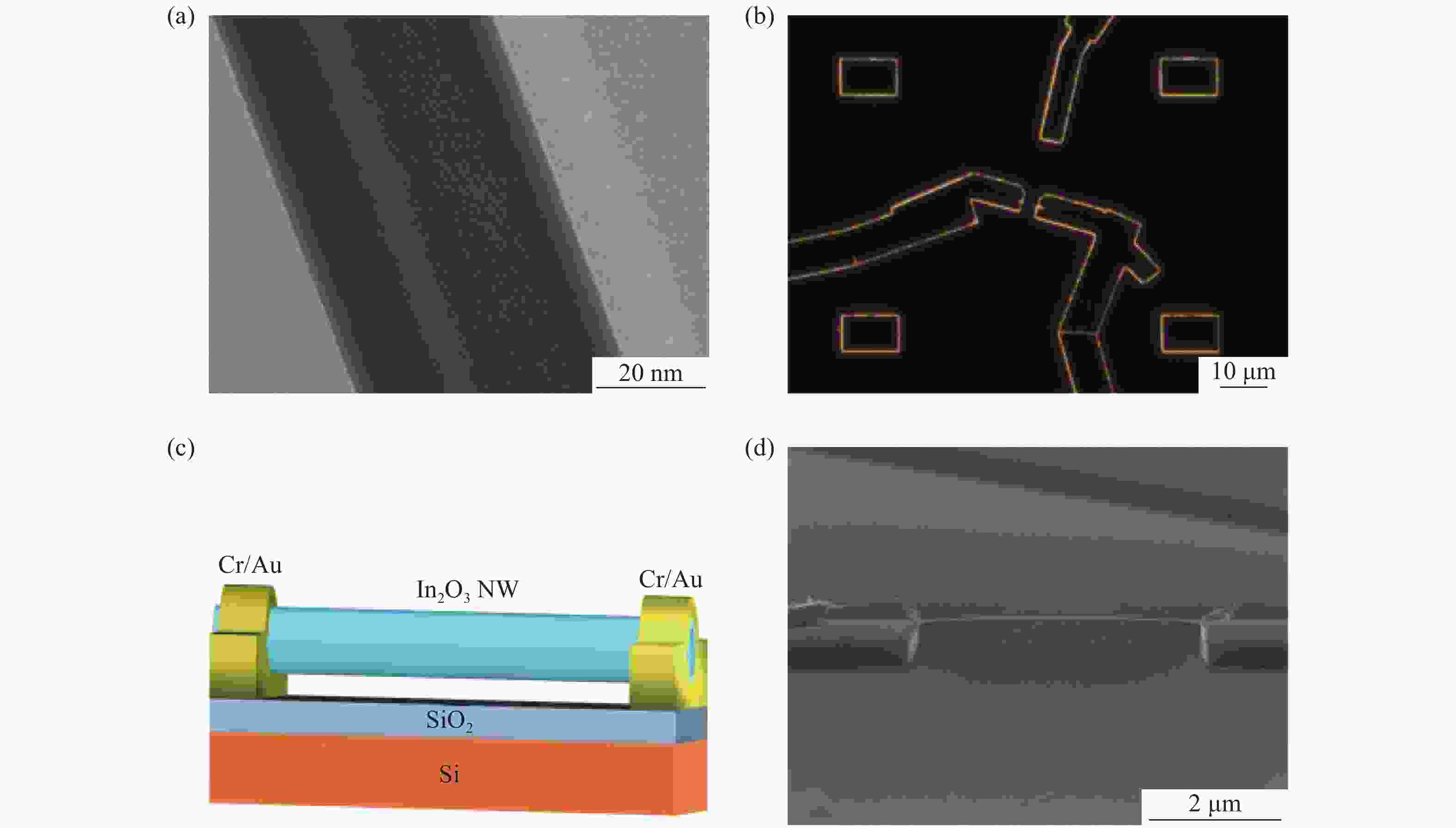
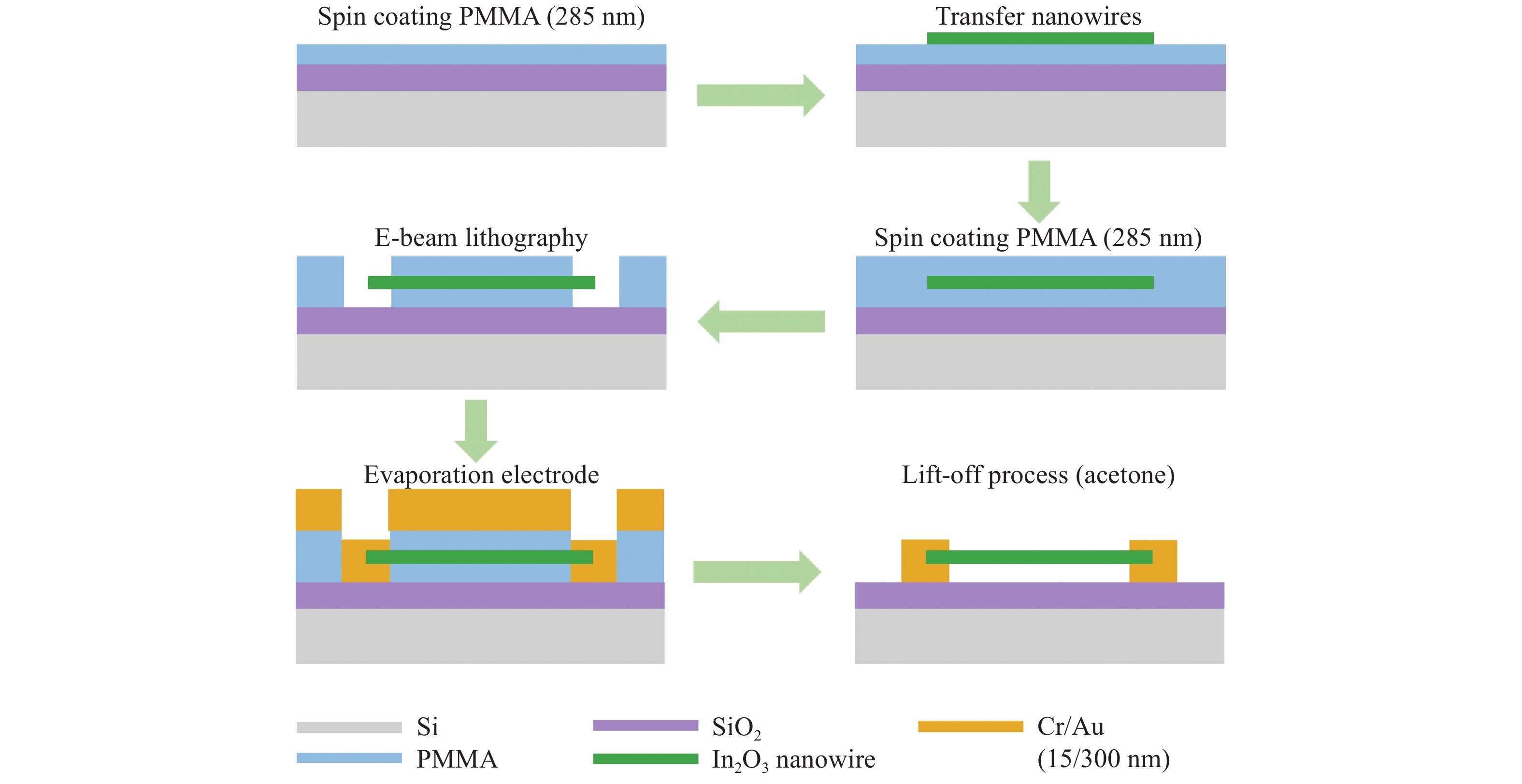
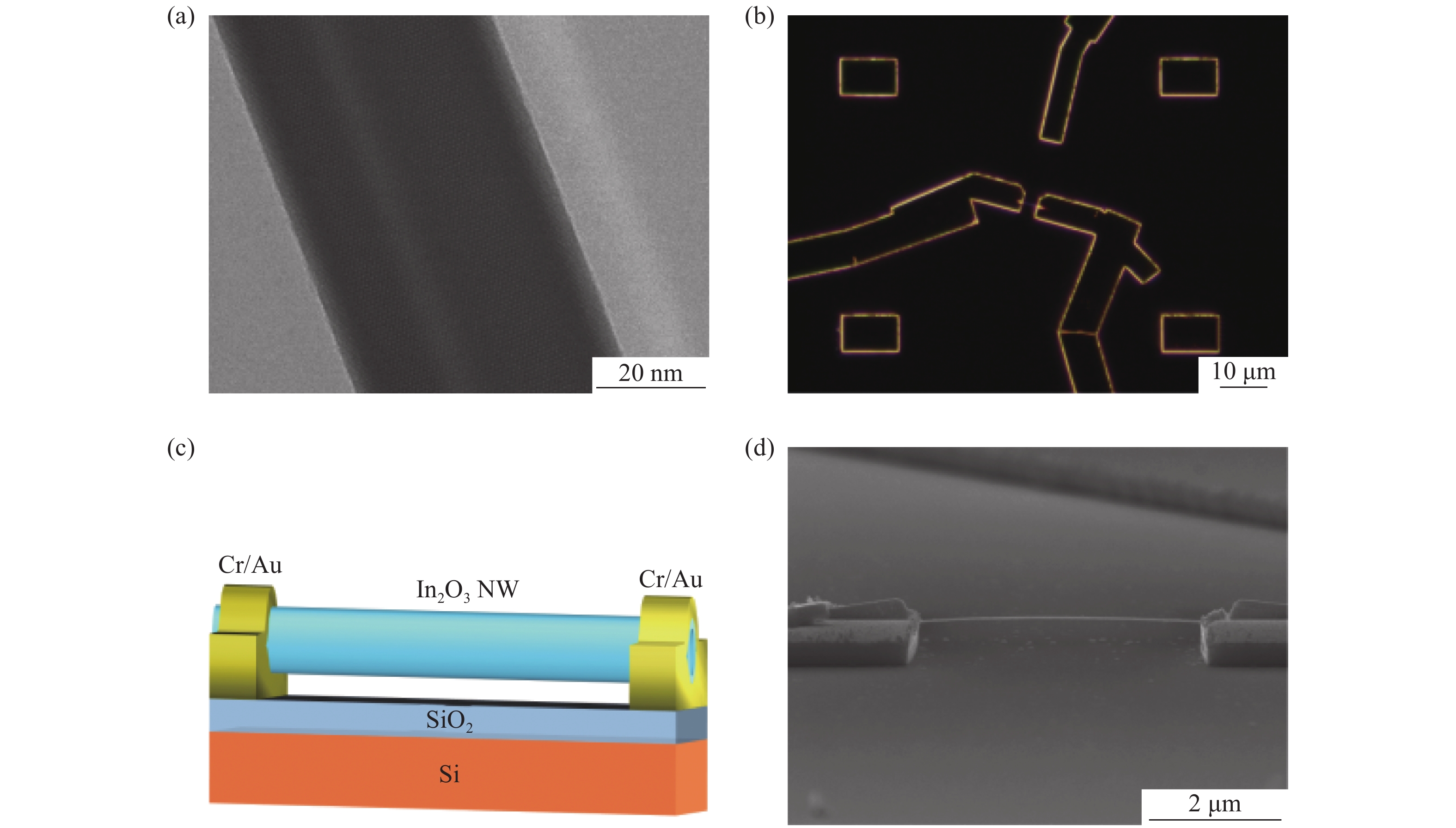
Figure 1. Design and characterization of the single In2O3 nanowire device. (a) TEM of a single In2O3 nanowire. (b) Dark-field microscopy image of an In2O3 nanowire FET. (c) Three-dimensional schematic view of a suspended single In2O3 nanowire photodetector. (d) SEM of the suspended single In2O3 nanowire photodetector
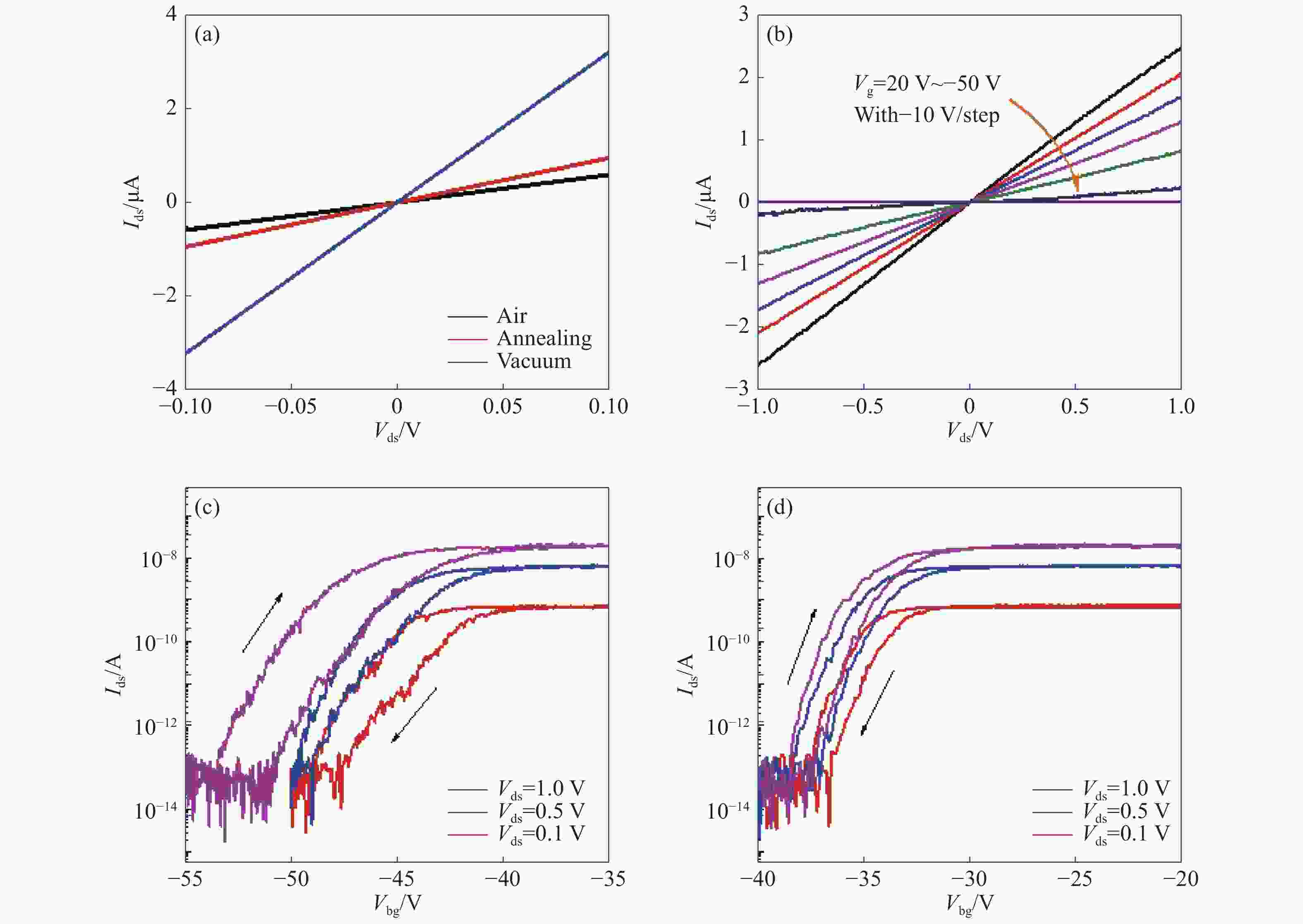
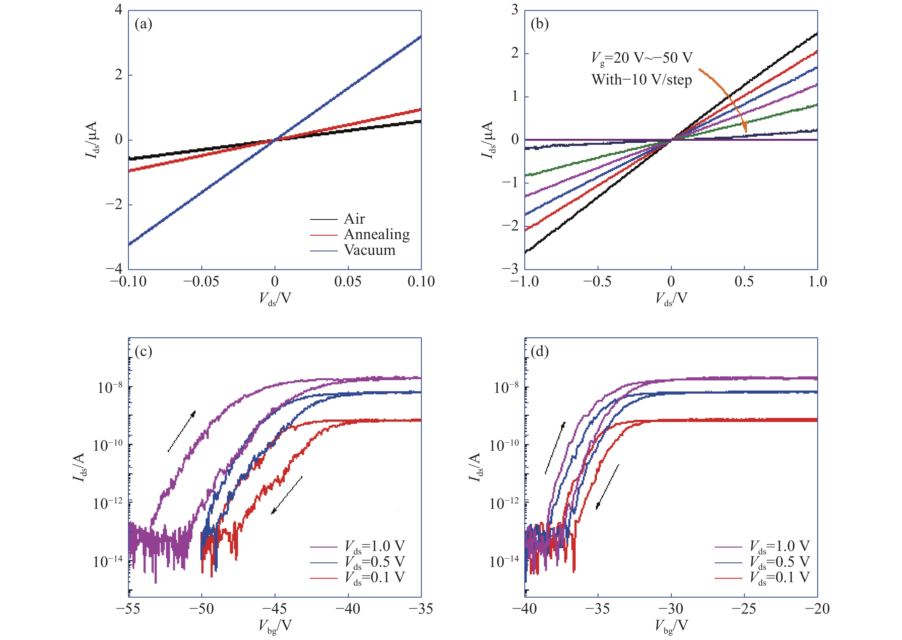
Figure 3. Electric performance of the single In2O3 nanowire devices under dark conditions. (a) I-V curves of the nanowire-based photodetector in different atmospheres. (b) Output characteristics of the nanowire-based photodetector under different gate voltages. Orange arrow represent that Vg is from 20 V to −50 V with −10 V steps. Transfer curve switch at different source-drain biases ranging from 0.1 V to 1 V (c) in the air and (d) in vacuum state. Black arrows represent the scanning direction of gate voltage.
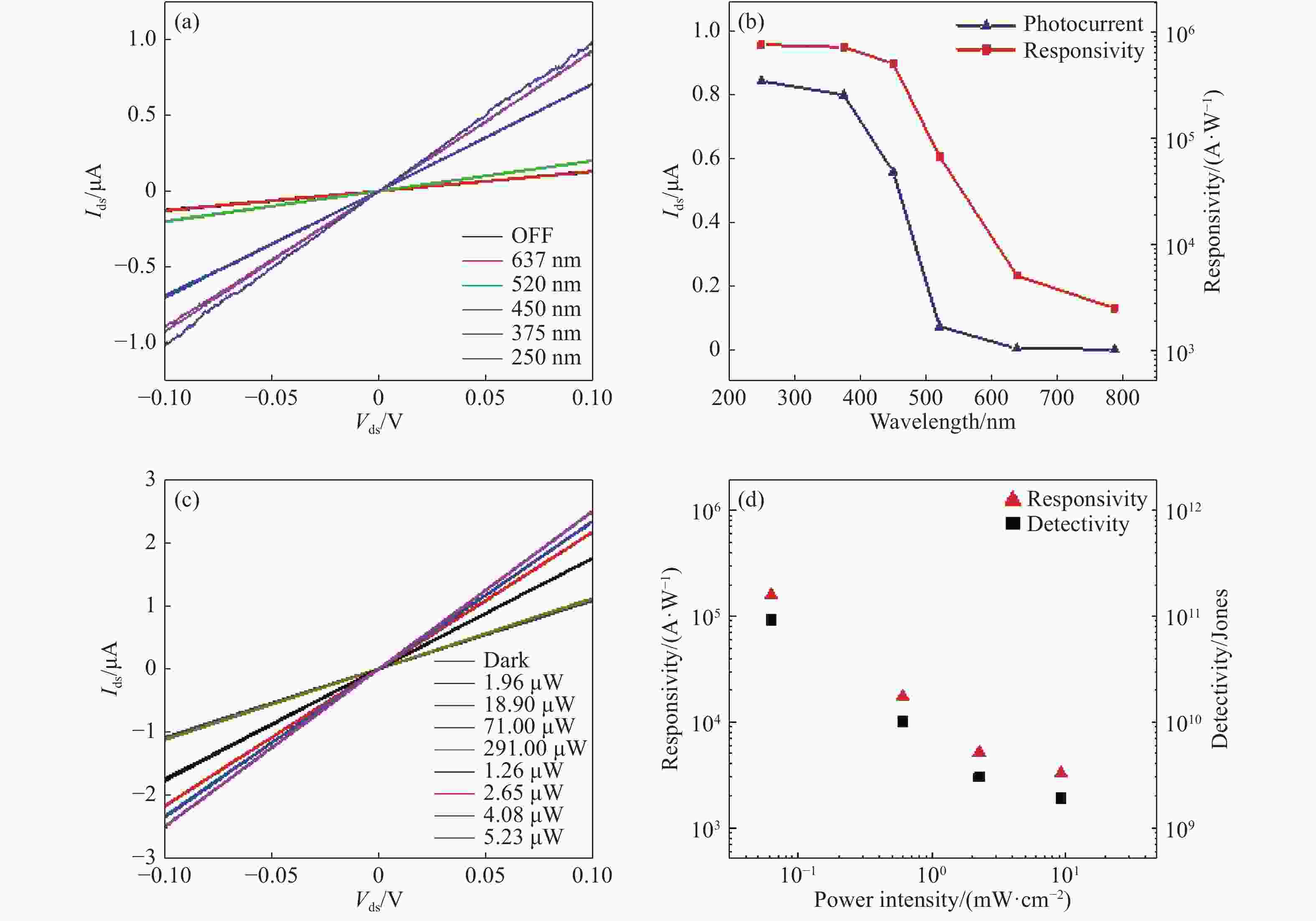
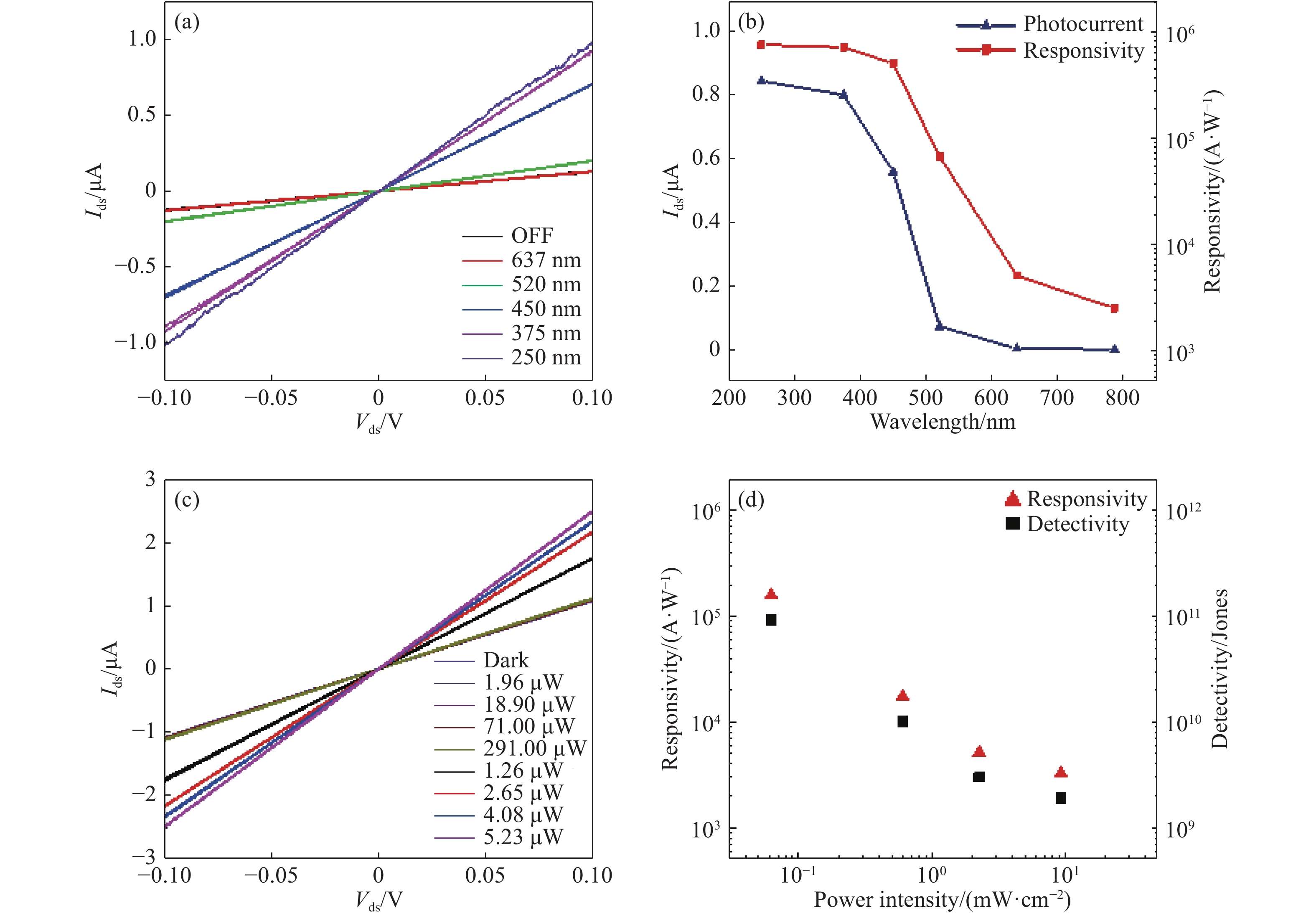
Figure 4. Photoresponse properties of the single In2O3 nanowire devices. (a) Ids-Vds characteristics of the photodetector in the dark and different wavelengths of light. (b) Photocurrent and responsivity of the photodetector under different wavelengths of light. (c) Ids-Vds characteristics of the photodetector in the dark and different intensities of light (450 nm). (d) Photoresponsivity and detectivity of the photodetector under the different intensities of light (450 nm).
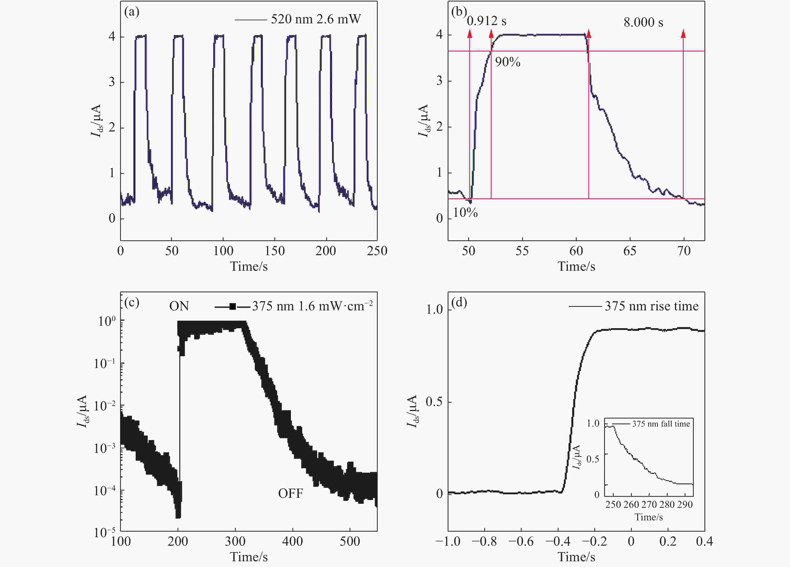
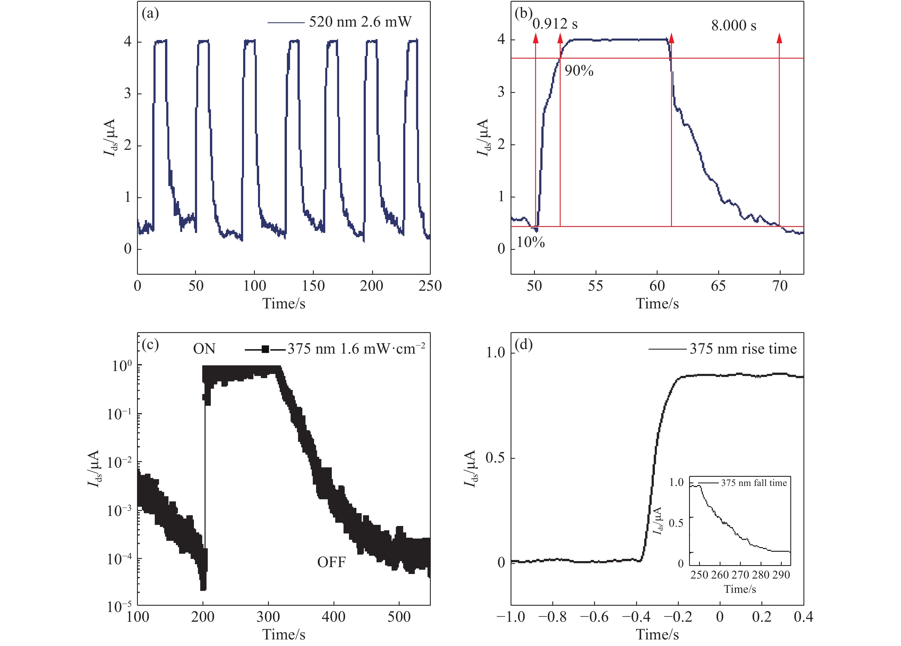
Figure 5. Time-response characterizations of the In2O3 single-nanowire photodetector. (a) Photocurrent response of the device, where the laser light is switched on/off at an interval of 20 s (520 nm, 2.6 mW·cm−2 at Vds = 1 V. (b) Enlargement of the curve in the 53~72 s range outlined in (a). (c) A single UV photocurrent response of the device (375 nm, 1.6 mW·cm−2). (d) Time-resolved photoresponse of the device showing the rise and fall time of the photocurrent at Vds = 0.1 V.
-
[1] HEO Y W, VARADARAJAN V, KAUFMAN M, et al. Site-specific growth of ZnO nanorods using catalysis-driven molecular-beam epitaxy[J]. Applied Physics Letters, 2002, 81(16): 3046-3048. doi: 10.1063/1.1512829 [2] JIANG W, WANG X D, CHEN Y, et al. Large-area high quality PtSe2 thin film with versatile polarity[J]. InfoMat, 2019, 1(2): 260-267. [3] YAN R X, GARGAS D, YANG P D. Nanowire photonics[J]. Nature Photonics, 2009, 3(10): 569-576. doi: 10.1038/nphoton.2009.184 [4] WU G J, TIAN B B, LIU L, et al. Programmable transition metal dichalcogenide homojunctions controlled by nonvolatile ferroelectric domains[J]. Nature Electronics, 2020, 3(1): 43-50. doi: 10.1038/s41928-019-0350-y [5] APPENZELLER J, KNOCH J, BJORK M T, et al. Toward nanowire electronics[J]. IEEE Transactions on Electron Devices, 2008, 55(11): 2827-2845. doi: 10.1109/TED.2008.2008011 [6] HONG W K, SOHN J I, HWANG D K, et al. Tunable electronic transport characteristics of surface-architecture-controlled ZnO nanowire field effect transistors[J]. Nano Letters, 2008, 8(3): 950-956. doi: 10.1021/nl0731116 [7] CUI Y, WEI Q Q, PARK H, et al. Nanowire nanosensors for highly sensitive and selective detection of biological and chemical species[J]. Science, 2001, 293(5533): 1289-1292. doi: 10.1126/science.1062711 [8] ZHENG G F, PATOLSKY F, CUI Y, et al. Multiplexed electrical detection of cancer markers with nanowire sensor arrays[J]. Nature Biotechnology, 2005, 23(10): 1294-1301. doi: 10.1038/nbt1138 [9] HUANG M H, MAO S, FEICK H, et al. Room-temperature ultraviolet nanowire nanolasers[J]. Science, 2001, 292(5523): 1897-1899. doi: 10.1126/science.1060367 [10] WAN Q, LI Q H, CHEN Y J, et al. Fabrication and ethanol sensing characteristics of ZnO nanowire gas sensors[J]. Applied Physics Letters, 2004, 84(18): 3654-3656. doi: 10.1063/1.1738932 [11] GOMES U P, ERCOLANI D, ZANNIER V, et al. Controlling the diameter distribution and density of InAs nanowires grown by Au-assisted methods[J]. Semiconductor Science and Technology, 2015, 30(11): 115012. doi: 10.1088/0268-1242/30/11/115012 [12] ROCCI M, DEMONTIS V, PRETE D, et al. Suspended InAs nanowire-based devices for thermal conductivity measurement using the 3ω method[J]. Journal of Materials Engineering and Performance, 2018, 27(12): 6299-6305. doi: 10.1007/s11665-018-3715-x [13] SU M, ZOU X M, GONG Y N, et al. Sub-kT/q switching in In2O3 nanowire negative capacitance field-effect transistors[J]. Nanoscale, 2018, 10(40): 19131-19139. doi: 10.1039/C8NR06163G [14] KONG Y C, YU D P, ZHANG B, et al. Ultraviolet-emitting ZnO nanowires synthesized by a physical vapor deposition approach[J]. Applied Physics Letters, 2001, 78(4): 407-409. doi: 10.1063/1.1342050 [15] YANG M, PANG G SH, JIANG L F, et al. Hydrothermal synthesis of one-dimensional zinc oxides with different precursors[J]. Nanotechnology, 2006, 17(1): 206-212. doi: 10.1088/0957-4484/17/1/034 [16] ZOU X M, LIU X Q, WANG C L, et al. Controllable electrical properties of metal-doped In2O3 nanowires for high-performance enhancement-mode transistors[J]. ACS Nano, 2013, 7(1): 804-810. doi: 10.1021/nn305289w [17] LIU Z W, ONG C, YU T, et al. Catalyst-free pulsed-laser-deposited ZnO nanorods and their room-temperature photoluminescence properties[J]. Applied Physics Letters, 2006, 88(5): 053110. doi: 10.1063/1.2168675 [18] ZHANG D H, LI C, HAN S, et al. Electronic transport studies of single-crystalline In2O3 nanowires[J]. Applied Physics Letters, 2003, 82(1): 112-114. doi: 10.1063/1.1534938 [19] MENG M, WU X L, JI X L, et al. Ultrahigh quantum efficiency photodetector and ultrafast reversible surface wettability transition of square In2O3 nanowires[J]. Nano Research, 2017, 10(8): 2772-2781. doi: 10.1007/s12274-017-1481-y [20] SHAO D L, QIN L Q, SAWYER S. Near ultraviolet photodetector fabricated from polyvinyl-alcohol coated In2O3 nanoparticles[J]. Applied Surface Science, 2012, 261: 123-127. doi: 10.1016/j.apsusc.2012.07.111 [21] ZHU H Y, WANG Y, XIAO J, et al. Observation of piezoelectricity in free-standing monolayer MoS2[J]. Nature Nanotechnology, 2015, 10(2): 151-155. doi: 10.1038/nnano.2014.309 [22] SU M, YANG ZH Y, LIAO L, et al. Side-Gated In2O3 nanowire ferroelectric FETs for high-performance nonvolatile memory applications[J]. Advanced Science, 2016, 3(9): 1600078. doi: 10.1002/advs.201600078 [23] KONSTANTATOS G, SARGENT E H. Nanostructured materials for photon detection[J]. Nature Nanotechnology, 2010, 5(6): 391-400. doi: 10.1038/nnano.2010.78 [24] ZHENG D SH, WANG J L, HU W D, et al. When nanowires meet ultrahigh ferroelectric field–high-performance full-depleted nanowire photodetectors[J]. Nano Letters, 2016, 16(4): 2548-2555. doi: 10.1021/acs.nanolett.6b00104 [25] GUO N, HU W D, LIAO L, et al. Anomalous and highly efficient InAs nanowire phototransistors based on majority carrier transport at room temperature[J]. Advanced Materials, 2014, 26(48): 8203-8209. doi: 10.1002/adma.201403664 [26] SOCI C, ZHANG A, XIANG B, et al. ZnO nanowire UV photodetectors with high internal gain[J]. Nano Letters, 2007, 7(4): 1003-1009. doi: 10.1021/nl070111x [27] GONG X, TONG M H, XIA Y J, et al. High-detectivity polymer photodetectors with spectral response from 300 nm to 1450 nm[J]. Science, 2009, 325(5948): 1665-1667. doi: 10.1126/science.1176706 [28] DAS K, MUKHERJEE S, MANNA S, et al. Single Si nanowire (diameter ≤ 100 nm) based polarization sensitive near-infrared photodetector with ultra-high responsivity[J]. Nanoscale, 2014, 6(19): 11232-11239. doi: 10.1039/C4NR03170A [29] LU J F, XU C X, DAI J, et al. Improved UV photoresponse of ZnO nanorod arrays by resonant coupling with surface plasmons of Al nanoparticles[J]. Nanoscale, 2015, 7(8): 3396-3403. doi: 10.1039/C4NR07114J [30] LOPEZ-SANCHEZ O, LEMBKE D, KAYCI M, et al. Ultrasensitive photodetectors based on monolayer MoS2[J]. Nature Nanotechnology, 2013, 8(7): 497-501. doi: 10.1038/nnano.2013.100 [31] HUANG S Y, OU G, CHENG J, et al. Ultrasensitive visible light photoresponse and electrical transportation properties of nonstoichiometric indium oxide nanowire arrays by electrospinning[J]. Journal of Materials Chemistry C, 2013, 1(39): 6463-6470. doi: 10.1039/c3tc31051e -

 下载:
下载:

计量
- 文章访问数: 2071
- HTML全文浏览量: 675
- PDF下载量: 109
- 被引次数: 0
