


Planar plasmonic lenses and their applications
-
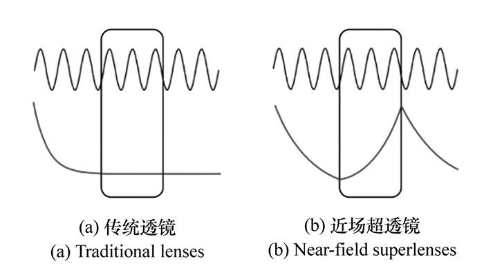
摘要: 由于衍射极限的存在,传统光学透镜成像分辨率理论上只能达到入射光波长的一半。通过恢复和增强携带物体细部特征信息的高频倏逝波,基于表面等离子体的平面金属透镜有望突破这种光学衍射极限,实现超分辨成像。本文对平面薄膜式与纳米结构式两类平面金属透镜进行了综述,详细介绍了若干典型平面金属透镜的结构设计、工作机理及其聚焦性能,并对其特点与存在的问题进行了分析与讨论。由于光波在金属中传播时存在一定损耗,如何更高效地增强高频倏逝波信号并转换成传播波,使其参与成像,以更好地实现远场超分辨成像,以及如何进一步增大近场超高分辨率聚焦光斑焦深以及减小远场聚焦光斑尺寸,是表面等离子体平面金属透镜进一步研究的重点。Abstract: The imaging resolution of conventional optical lenses is generally restricted to half the incident wavelength by the diffraction limit due to the decay of evanescent waves. Planar metallic lenses based on surface plasmons offer the possibility to overcome this limit by the enhancement of evanescent waves which carrying detailed feature information of object. In this paper, the structural design, physical mechanism and focusing performance of two types of typical planar metallic lenses are reviewed. Moreover, the existing problems in this imaging technology are discussed. Because there is a certain loss when the light propagates in the metal, how to more effectively enhance the high frequency evanescent wave signal and convert it to propagation wave which can participate in the imaging in order to better achieve the far-field super-resolution imaging, and how to further increase the ultra high resolution near-field focal depth of focusing spot and reduce size of the far-field focusing spot, are further research focuses of the surface plasmonic planar metallic lenses.
-

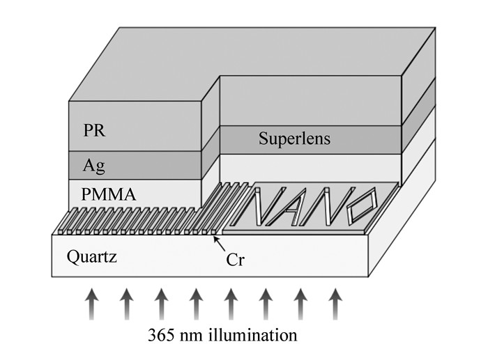
图 2 银膜超透镜超分辨成像实验示意图
Figure 2. Schematic diagram of a silver film optical superlensing experiment

图 3 纳米狭缝阵列成像对比。(a) 原子力显微镜测得的基于银膜超透镜的成像结果及其 (c) 截面轮廓图,(b) 利用35 nm厚的PMMA薄膜替代金属银膜后的成像结果及其 (d) 截面轮廓图
Figure 3. Comparison of the images for an array of 60-nm-wide slots with and without silver superlens. (a) AFM picture of the developed image recorded with the silver superlens and (c) its profile of height. (b) AFM picture of the developed image recorded without the silver superlens, whilst 35-nm-thick PMMA layer instead, and (d) its profile of height

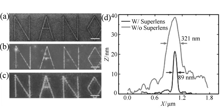
图 4 任意纳米结构“NANO”成像对比。(a) FIB加工的“NANO”结构。(b) 基于银膜超透镜实现的成像结果。(c) 利用35 nm厚的PMMA薄膜替代金属银膜后的成像结果。(d) 不同成像系统中,字母“A”的像线宽
Figure 4. Comparison of the images for an arbitrary object "NANO" with and without silver superlens. (a) FIB fabricated result of the object. The linewidth of the "NANO" object was 40 nm. (b) AFM of the developed image on photoresist with a silver superlens. (c) AFM of the developed image on photoresist when the 35-nm-thick layer of silver was replaced by PMMA spacer as a comparative experiment. (d) Averaged cross section of letter "A" shows an exposed line width of 89 nm (black line), whereas for the PMMA spacer, it is 321±10 nm (gray line)

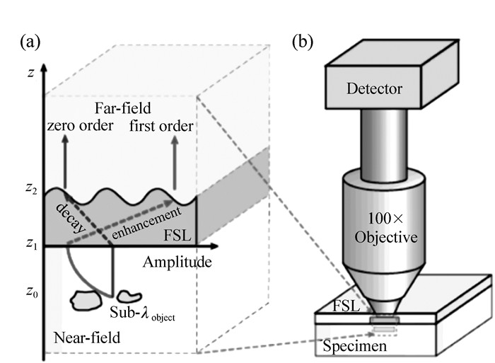
图 5 (a) 由亚波长光栅结构和银膜构成的远场超透镜及其工作原理, (b) 远场超透镜显微成像系统
Figure 5. (a) A far-field superlens (FSL) constructed by adding a subwavelength grating onto a silver slab superlens. (b) A FSL microscope

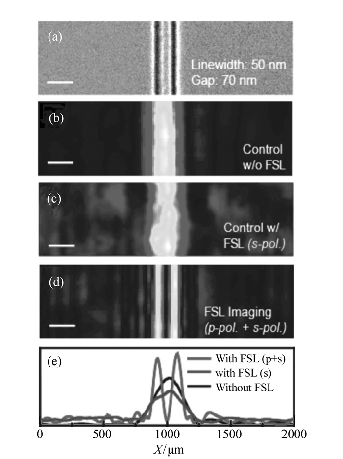
图 6 一对纳米狭缝的远场成像。(a) FIB加工的一对纳米狭缝。(b) 传统光学显微镜成像。(c) 在s极化光作用下,远场超透镜成像。(d) 在s和p极化光作用下,远场超透镜成像。(e) 不同情况下像的截面轮廓对比
Figure 6. Far-field imaging of a pair of nanoslits. (a) A pair of nanoslits fabricated by FIB on a 40 nm thick Cr film on the quartz substrate. (b) Diffraction-limited image from a conventional optical microscoped. (c) FSL image with s-polarized incident light, which is still diffraction limited due to the lack of surface-plasmon-assisted evanescent enhancementd. (d) FSL image combining both s-and p-polarized incident lights that resolves the sub-diffraction-limit objects due to the strong enhancement of evanescent waves via efficient surface plasmon excitation. (e) Intensity profiles of the images as given above in (b), (c) and (d)

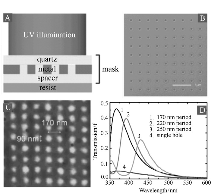
图 7 亚波长圆孔式平面金属透镜及其光刻应用。(a) 圆孔式平面金属透镜光刻示意图。(b) FIB加工的圆孔阵列式掩膜。(c) 原子力显微镜测得的成像结果。(d) 结构透过率与入射波长之间关系
Figure 7. Plasmonic lens formed by subwavelength nanohole arrays perforated in a metal film and its application to optical nanolithography. (a) Schematic of the plasmonic lithography. (b) FIB image of a hole array mask. (c) AFM image of the array pattern. (d) Spectrum measurements of far-field transmission through the hole array

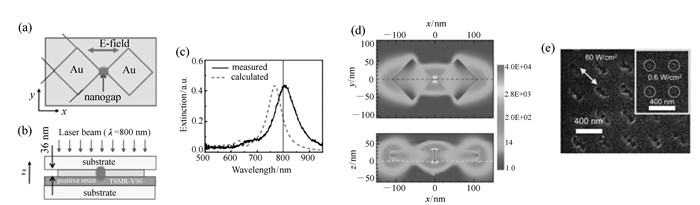
图 8 蝴蝶结型平面金属透镜结构及其聚焦性能的仿真与实验。(a) 蝴蝶结型金纳米结构。(b) 利用蝴蝶结型纳米结构进行光刻实验的示意图。(c) 实验与仿真得到的蝴蝶结型金纳米结构阵列光传输特性。(d) 仿真计算的场强分布。(e) 蝴蝶结型平面金属透镜实现的光刻图形
Figure 8. (a, b) Design of a gold bowtie nanostructure and its schematic realization of the photolithographical experiment. (c) Experimental and calculated transmissive spectra of an array of gold bowtie nanostructures. (d) Calculated field intensity patterns. (e) SEM image of the developed positive photoresist after exposing by the array of gold bowtie nanostructures

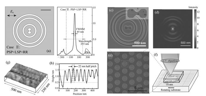
图 9 复合结构平面金属透镜及其在光刻系统中的应用。(a) 复合结构平面金属透镜设计。(b) 仿真得到的透镜出射场10 nm处x轴上的光强分布。(c) FIB加工的复合结构表面等离子体透镜。(d) 透镜出射场10 nm处的光强分布。(e) FIB加工的透镜阵列。(f) 表面等离子体浮动磁头。(g) 光刻胶显影结果。(h) 显影得到的截面轮廓
Figure 9. Plasmonic lens formed by the hybrid nanostructures and its application to high-throughput maskless nanolithography. (a) Design of the plasmonic lens composed of hybrid nanostructures. (b) Simulated light intensity profile at the plane 10 nm away from the lens. (c) SEM picture of the fabricated plasmonic lens. (d) Field intensity distribution. (e) SEM image of an array of the designed plasmonic lens. (f) A flying head containing the plasmonic lens. (g) AFM image of the developed photoresist, and (h) its cross-sectional profile showing the resolution approaching to 22 nm

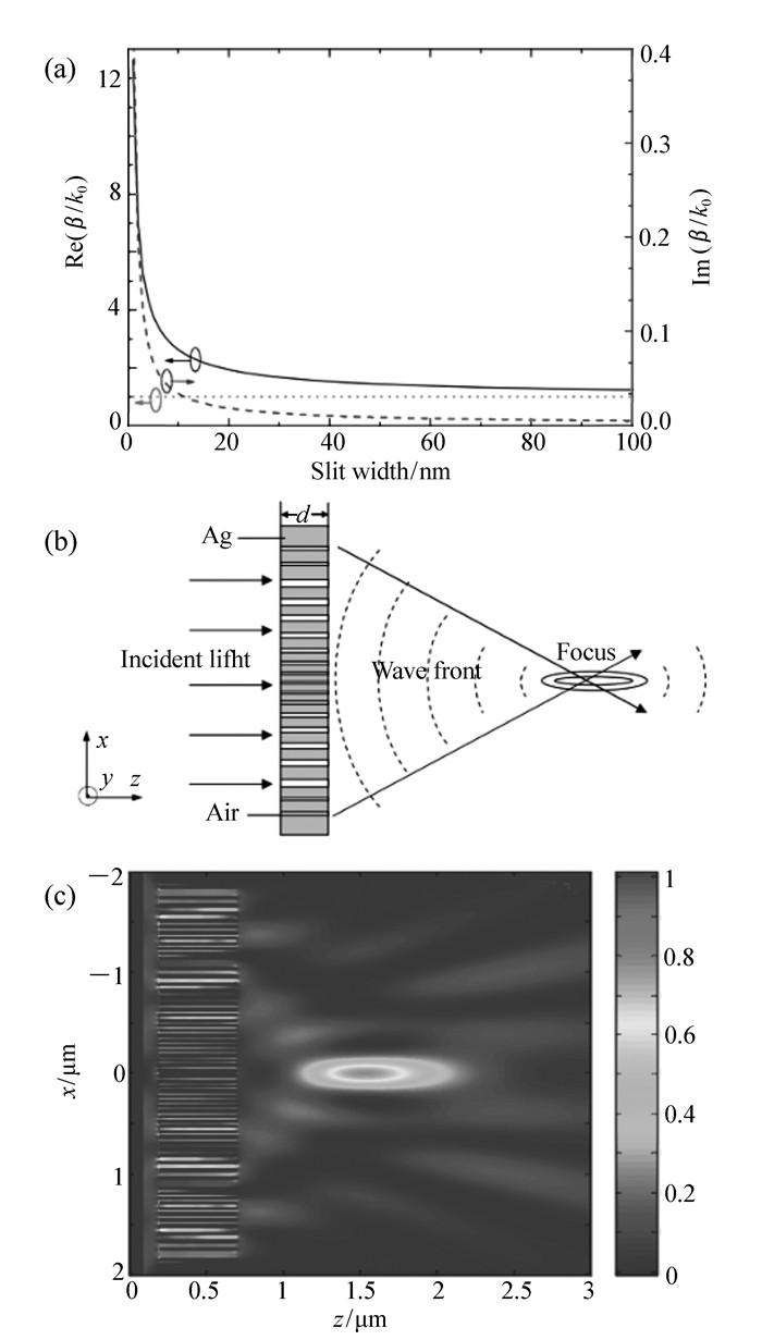
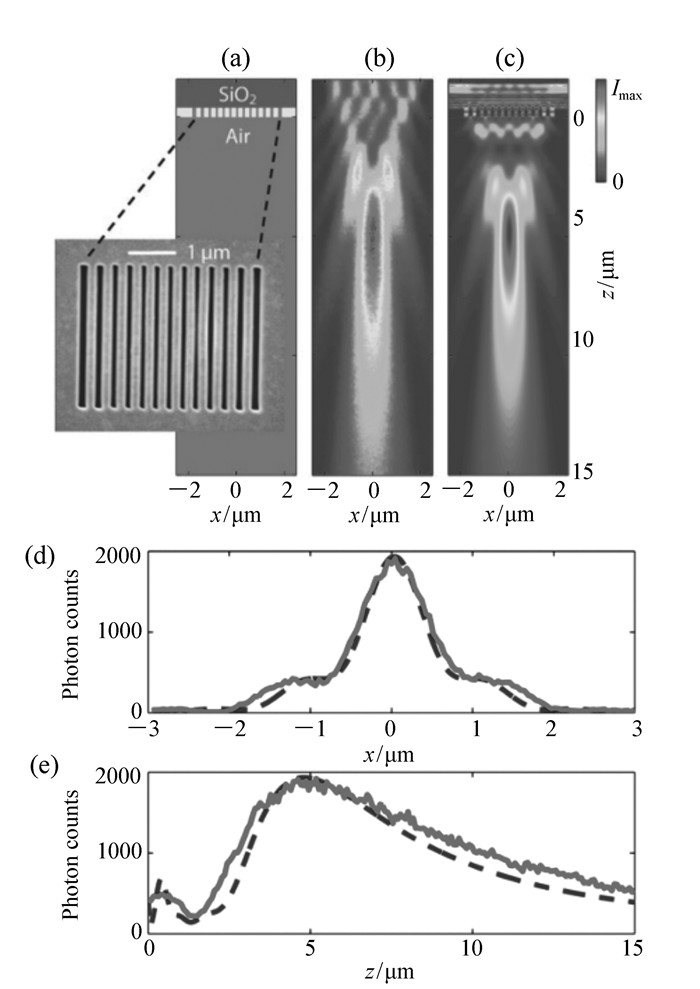
图 10 (a) 光在纳米狭缝中传播常数与狭缝宽度之间的关系。(b) 纳米狭缝式平面金属透镜设计原理。(c) FDTD仿真得到的透镜聚焦性能。工作波长为650 nm
Figure 10. (a) Dependence of propagation constant on slit width. (b) Schematic of the plasmonic lens formed by a nanoslit array in a silver film. (c) FDTD calculated result of the normalized Poynting Vector Sz for a designed lens

图 11 (a) 基于FIB技术加工的纳米狭缝式平面金膜透镜,金膜厚度为400 nm。(b) 共聚焦显微镜测得的透镜聚焦性能。(c) FDFD仿真得到的透镜聚焦性能。(d) 与 (e) 透镜焦点半高宽与焦距的仿真值与实验值对比
Figure 11. (a) Geometry of the lens consisting of a 400 nm thick gold film (yellow) with nanoslits of different widths milled therein on a fused silica substrate. (b) Focusing pattern measured by the confocal scanning optical microscopy (CSOM). (c) FDFD simulated focusing pattern. Simulated (dashed blue line) and CSOM measured (solid red line) light intensity in cross sections of the focus along the x direction (d) and z direction (e)

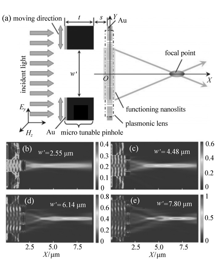
图 12 (a) 利用可调微机械狭缝实现对表面等离子体透镜聚焦性能主动控制的结构示意图。(b)~(e) 狭缝宽度分别为2.55,4.48,6.14,7.80 μm时的透镜光场分布。工作波长为650 nm,透镜设计焦距为5 μm
Figure 12. (a) Schematic of an active plasmonic lens with a micromechanical tunable pinhole located ahead of the plasmonic lens. FDTD simulated electric-field intensity for the plasmonic lens with different pinhole width w′: (b)w′=2.25 μm, (c)w′=4.48 μm, (d)w′=6.14 μm, (e)w′=7.80 μm. The operating wavelength is 650 nm and the designed focal length for the plasmonic lens is 5 μm

图 13 (a) 十字形通孔式平面金属透镜。其中,阵列中十字形通孔呈轴对称,通孔中心间距与宽度w固定不变,长度l可变。(b) 透过率以及 (c) 光在十字形通孔中传输的相位延迟与入射光波长和通孔几何形状之间的关系
Figure 13. (a) Schematic of a planar plasmonic lens formed by the cross-shaped aperture arrays of periodicity p in a thin silver film. The symmetric aperture has a fixed arm-width, w, and a spatially modulated arm length, l. (b) Transmittance and (c) phase variation of light passing through an array of cross-shaped apertures in a silver film as a function of wavelength and arm length of the crosses

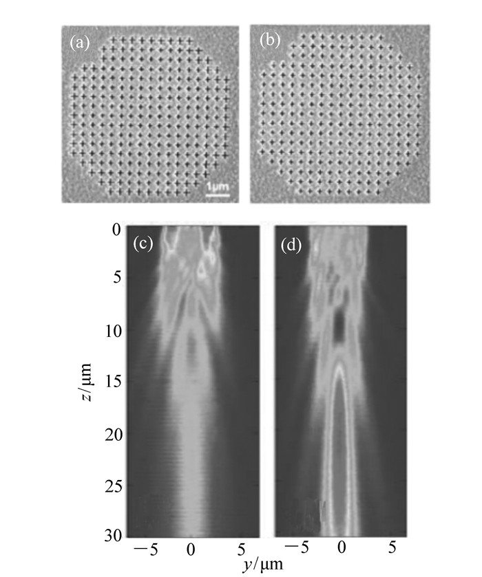
图 14 (a) 与 (b) 分别为设计焦距15 μm与25 μm的十字形通孔式平面金属银透镜。(c) 和 (d) 分别为两个透镜y-z平面光强分布。工作波长为850 nm
Figure 14. (a) and (b) SEM images of the fabricated cross-shaped aperture silver lens devices with the designed focal length fd=15 μm and 25 μm, respectively. (c) and (d) Experimentally measured axial light intensity profile (on the y-z plane) for the lenses with fd=15 μm and 25 μm, respectively. The samples were illuminated by the 850 nm wavelength

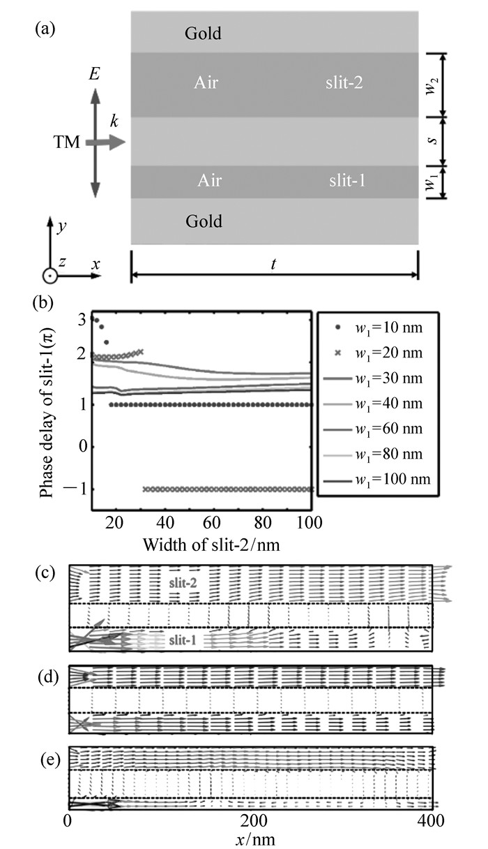
图 15 (a) 相邻纳米狭缝 (slit-1与slit-2) 结构示意图。w1与w2分别为狭缝slit-1与狭缝slit-2的宽度,s为两狭缝间距。(b) 狭缝slit-2对slit-1相位延迟影响规律,其中,两狭缝金属间距为30 nm。(c)~(e) 狭缝slit-1、slit-2和金属隔墙中坡印廷矢量分布。(c)w1=20 nm, w2=40 nm; (d)w1=20 nm, w2=30 nm; (e)w1=10 nm, w2=20 nm
Figure 15. (a) Schematic of two coupled nanoslits in a 400 nm thick gold film. (b) Effect of slit-2 on the phase delay of slit-1, the gold spacing s is 30 nm. (c)~(e) Poynting vector in the two nanoslits and the gold wall between them is 30 nm. (c)w1=20 nm, w2=40 nm. Light in slit-1 propagates backwards at the exit of the structure. (d)w1=20 nm, w2=30 nm. Light can normally pass through slit-1. (e)w1=10 nm, w2=20 nm. The optical transmission in slit-1 is locally off

图 16 金属隔墙对狭缝slit-1的相位延迟影响。其中,w1=10 nm,w2=60 nm
Figure 16. Change of the phase delay of slit-1 with the gold spacing between slit-1 and slit-2. w1=10 nm, w2=60 nm

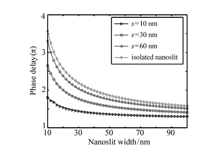
图 17 不同金属隔墙的周期性波导阵列中狭缝相位延迟与狭缝宽度之间的关系。t=400 nm
Figure 17. Dependence of phase delay on the nanoslit width. t=400 nm

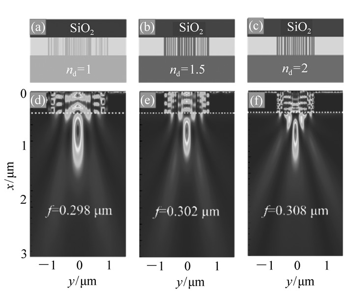
图 18 基于不同工作介质设计的表面等离子体透镜,(a) 透镜工作介质为空气,(b) 透镜工作介质折射率为1.5,(c) 透镜工作介质折射率为2, (d)~(f) 分别为图 18(a)~(c)中透镜聚焦性能
Figure 18. Plasmonic lenses working in different refractive-index dielectrics for the designed focal length of 0.3 m at a wavelength of 650 nm, (a) lens working in air, (b) lens working in a dielectric with refractive index equal to 1.5, (c) lens working in a dielectric with refractive index equal to 2, (d)~(f) focusing performance for the lenses in Fig. 18(a)~18(c), respectively

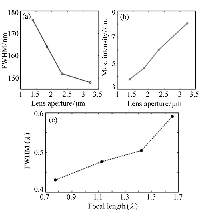
图 19 (a) 透镜焦点半高宽FWHM与透镜尺寸之间的关系。(b) 透镜尺寸对透镜焦点光强的影响。(c) 透镜焦距对焦点半高宽FWHM的影响
Figure 19. (a) Dependence of the focal spot size on the lens aperture. (b) Effect of the lens aperture on light intensity. (c) Effect of the focal length on the focal spot size

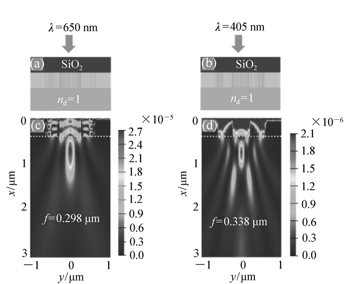
图 20 (a) 工作波长为650 nm的耦合纳米狭缝式平面金属透镜。(b) 工作波长为405 nm的平面金属透镜。(c) 和 (d) 分别为两个透镜光场分布,其中,透镜设计焦距为0.3 μm
Figure 20. (a) Lens operating at 650 nm. (b) Lens operating at 405 nm. (c), (d) Focusing performance for the lenses in Fig. 20(a) and Fig. 20(b), the designed focal length is 0.3 μm

图 21 (a) FIB技术加工的纳米狭缝式平面金膜透镜。(b) 实验测得的透镜出射场光场分布。(c) 实验测得的焦点大小
Figure 21. (a) A plasmonic lens consisting of an array of nanoslits in a gold film fabricated by FIB. (b) Measured Focusing pattern. (c) Measured focal spot size

图 22 超振荡透镜超分辨成像 (a) 超振荡透镜,(b)~(c) 仿真计算的透镜光场分布。(d) 和 (e) 分别为112 nm宽狭缝及其超振荡透镜成像结果。(f) 两目标狭缝,(g) 和 (h) 分别为两狭缝的超振荡透镜成像与传统显微镜成像结果对比
Figure 22. Subwavelength imaging by a super-oscillatory lens (SOL). (a) SEM image of the SOL. (b) calculated energy distribution of the lens at 10.3 μm. (c) Enlarged focal point, λ=640 nm. (d) SEM image of a 112 nm slit, and (e) image by SOL. A double slit (f) and its SOL image (g). (h) Image of the same double slit is not resolved using a conventional lens of NA=1.4
表 1 透镜尺寸对设计焦距为3 μm透镜聚焦性能的影响
Table 1. Effect of the lens size on the focusing performance when the designed focal length equals to 3 μm
透镜孔径/μm 总相位差 (π) 实际焦距/μm FWHM/μm 2.28 0.6 1.820 0.89λ 3.31 1.28 2.202 0.87λ 4.13 1.94 2.602 0.79λ 4.78 2.51 2.806 0.76λ  下载: 导出CSV
表 2 不同工作介质中表面等离子体透镜聚焦性能
Table 2. Derived focusing performance for the designed lenses working in different refractive-index dielectrics
工作介质折射率 透镜孔径 FWHM/nm 最大光强/a.u. 1 1.852 250(λ/2.60) 2.684 4 1.5 1.394 176(λ/3.69) 3.767 8 2 1.152 134(λ/4.85) 1.299 4
下载: 导出CSV
-
[1] BORN M, WOLF E. Principles of Optics[M]. Cambridge University Press, 1999. [2] AUGUSTIN T, BHENDE S, CHAVDA K, et al.. Scanning near-field optical microscopy with aperture probes:fundamentals and applications[J]. J. Chem. Phys., 2000, 112(18):7761-7774. doi: 10.1063/1.481382 [3] BARNES W L, DEREUX A, EBBESEN T W. Surface plasmon subwavelength optics[J]. Nature, 2003, 424(6950):824-830. doi: 10.1038/nature01937 [4] PENDRY J B, HOLDEN A J, ROBBINS D J, et al.. Low frequency plasmons in thin-wire structures[J]. J. Phys. Condens. Matter, 1998, 10(22):4785-4809. doi: 10.1088/0953-8984/10/22/007 [5] 陈泳屹, 佟存柱, 秦莉, 等.表面等离子体激元纳米激光器技术及应用研究进展[J].中国光学, 2012, 5(5):453-463. http://www.chineseoptics.net.cn/CN/abstract/abstract8877.shtmlCHEN Y Y, TONG C ZH, QIN L, et al.. Progress in surface plasmon polariton nano-laser technologies and applications[J]. Chinese Optics, 2012, 5(5):453-463.(in Chinese) http://www.chineseoptics.net.cn/CN/abstract/abstract8877.shtml [6] 蔡浩原.高分辨率表面等离子体显微镜综述[J].中国光学, 2014(5):691-700. http://www.chineseoptics.net.cn/CN/abstract/abstract9180.shtmlCAI H Y. Review of high resolution surface plasmon microscopy[J]. Chinese Optics, 2014(5):691-700.(in Chinese) http://www.chineseoptics.net.cn/CN/abstract/abstract9180.shtml [7] PENDRY J B. Negative refraction makes a perfect lens[J]. Phys. Rev. Lett., 2000, 85(18):3966-3969. doi: 10.1103/PhysRevLett.85.3966 [8] FANG N, LEE H, SUN C, et al.. Sub-diffraction-limited optical imaging with a silver superlens[J]. Science, 2005, 308:534-537. doi: 10.1126/science.1108759 [9] ZHANG X, LIU Z. Superlenses to overcome the diffraction limit[J]. Nat. Mater., 2008, 7(6):435-41. doi: 10.1038/nmat2141 [10] UENO K, TAKABATAKE S, NISHIJIMA Y, et al.. Nanogap-assisted surface plasmon nanolithography[J]. J. Phys. Chem. Lett., 2010, 1(3):657-662. doi: 10.1021/jz9002923 [11] PAN L, PARK Y, XIONG Y, et al.. Maskless plasmonic lithography at 22 nm resolution[J]. Sci. Rep., 2011, 1(11):116-120. https://www.researchgate.net/publication/221852473_Maskless_Plasmonic_Lithography_at_22_nm_Resolution [12] GAO H, HYUN J K, LEE M H, et al.. Broadband plasmonic microlenses based on patches of nanoholes[J]. Nano Lett., 2010, 10(10):4111-4116. doi: 10.1021/nl1022892 [13] YU Y, CHASSAING D, SCHERER T, et al.. The focusing and talbot effect of periodic arrays of metallic nanoapertures in high-index medium[J]. Plasmonics, 2013, 8(2):723-732. doi: 10.1007/s11468-012-9463-0 [14] SHI H, WANG C, DU C, et al.. Beam manipulating by metallic nano-slits with variant widths[J]. Opt. Express, 2005, 13(18):6815-6820. doi: 10.1364/OPEX.13.006815 [15] VERSLEGERS L, CATRYSSE P B, YU Z, et al.. Planar lenses based on nanoscale slit arrays in a metallic film[J]. Nano Lett., 2009, 9(1):235-238. doi: 10.1021/nl802830y [16] LIN L, GOH X M, MCGUINNESS L P, et al.. Plasmonic lenses formed by two-dimensional nanometric cross-shaped aperture arrays for Fresnel-region focusing[J]. Nano Lett., 2010, 10(5):1936-1940. doi: 10.1021/nl1009712 [17] YU Y, ZAPPE H. Effect of lens size on the focusing performance of plasmonic lenses and suggestions for the design[J]. Opt. Express, 2011, 19(10):9434-9444. doi: 10.1364/OE.19.009434 [18] YU Y, ZAPPE H. Theory and implementation of focal shift of plasmonic lenses[J]. Opt. Lett., 2012, 37(9):1592-1594. doi: 10.1364/OL.37.001592 [19] ZHANG Y, FU Y, LIU Y, et al.. Experimental study of metallic elliptical nano-pinhole structure-based plasmonic lenses[J]. Plasmonics, 2011, 6(2):219-226. doi: 10.1007/s11468-010-9191-2 [20] FU Y, LIU Y, ZHOU X, et al.. Experimental investigation of superfocusing of plasmonic lens with chirped circular nanoslits[J]. Opt. Express, 2010, 18(4):3438-3443. doi: 10.1364/OE.18.003438 [21] LIU Y, FU Y, ZHOU X, et al.. Experimental study of indirect phase tuning-based plasmonic structures for finely focusing[J]. Plasmonics, 2011, 6(2):227-233. doi: 10.1007/s11468-010-9192-1 [22] ZHU Y, YUAN W, YU Y, et al.. Metallic planar lens formed by coupled width-variable nanoslits for superfocusing[J]. Opt. Express, 2015, 23(15):20124-20131. doi: 10.1364/OE.23.020124 [23] 史林兴, 王莉, 李华, 等.表面等离子体激元透镜设计及其数值计算[J].光学精密工程, 2010, 18(3):831-835. http://www.cnki.com.cn/Article/CJFDTOTAL-GXJM201003029.htmSHI L X, WANG L, LI H, et al.. Design and numerical simulation of plasmon polariton nanolens[J]. Opt. Precision Eng., 2010, 18(4):831-835.(in Chinese) http://www.cnki.com.cn/Article/CJFDTOTAL-GXJM201003029.htm [24] DURANT S, LIU Z, STEELE J M, et al.. Theory of the transmission properties of an optical far-field superlens for imaging beyond the diffraction limit[J]. J. Opt. Soc. Am. B, 2006, 23(11):2383-2392. doi: 10.1364/JOSAB.23.002383 [25] LIU Z, DURANT S, LEE H, et al.. Far-field optical superlens[J]. Nano Lett., 2007, 7(2):403-408. doi: 10.1021/nl062635n [26] SRITURAVANICH W, FANG N, SUN C, et al.. Plasmonic nanolithography[J]. Nano Lett., 2004, 4(6):1085-1088. doi: 10.1021/nl049573q [27] MART NMORENO L, GARC AVIDAL F J, LEZEC H J, et al.. Theory of extraordinary optical transmission through subwavelength hole arrays[J]. Nature, 2001, 86(6):667-669. https://www.researchgate.net/publication/12152854_Theory_of_Extraordinary_Optical_Transmission_through_Subwavelength_Hole_Arrays [28] WANG L, UPPULURI S M, JIN E X, et al.. Nanolithography using high transmission nanoscale bowtie apertures[J]. Nano Lett., 2006, 6(3):361-364. doi: 10.1021/nl052371p [29] SUNDARAMURTHY A, SCHUCK P J, CONLEY N R, et al.. Toward nanometer-scale optical photolithography:utilizing the near-field of bowtie optical nanoantennas[J]. Nano Lett., 2006, 6(3):355-360. doi: 10.1021/nl052322c [30] ZHU Y, YUAN W, YU Y, et al.. Robustly efficient superfocusing of immersion plasmonic lenses based on coupled nanoslits[J]. Plasmonics, 2016, DOI: 10.1007/s11468-016-0208-3. [31] ZHU Y, YUAN W, YU Y, et al.. Exploring the superfocusing performance of plasmonic lenses formed by coupled nanoslits[J]. Micro Nano Lett., 2016, DOI: 10.1049/mnl.2016.0288. [32] ROGERS E T, LINDBERG J, ROY T, et al.. A super-oscillatory lens optical microscope for subwavelength imaging[J]. Nat. Mater., 2012, 11(5):432-435. doi: 10.1038/nmat3280 [33] DIAO J, YUAN W, YU Y, et al.. Controllable design of super-oscillatory planar lenses for sub-diffraction-limit optical needles[J]. Opt. Express, 2016, 24(3):1924-1933. doi: 10.1364/OE.24.001924 [34] YU Y, WANG P, ZHU Y, et al.. Broadband metallic planar microlenses in an array:the focusing coupling effect[J]. Nanoscale Res. Lett., 2016, 11(1):1-10. doi: 10.1186/s11671-015-1209-4 -

 下载:
下载:


 点击查看大图
计量
- 文章访问数: 2883
- HTML全文浏览量: 650
- PDF下载量: 1151
- 被引次数: 0
